
In college many of us dreamed of starting up our own company by offering something new that has never been done before. Today I spoke by phone with Yunshan Zhuin Shanghai, and he has actually lived out this scenario by founding NextOp in 2006, then getting that company acquired by Atrentain 2012. The new capability that NextOp created… Read More

Author: Daniel Payne
FinFET Design for Power, Noise and Reliability

IC designers have been running analysis tools for power, noise and reliability for many years now, so what is new when you start using FinFET transistors instead of planar transistors? Calvin Chow from ANSYS (Apache Design) presented on this topic earlier in the summer through a 33 minutewebinar that has been archived. There is… Read More
Transistor-level Sizing Optimization
RTL designers know that their code gets transformed into gates and cells by using a logic synthesis tool, however these gates and cells are further comprised of transistors and sometimes you really need to optimize the transistor sizing to reach power, performance and area goals. I’ve done transistor-level IC design before,… Read More
FinFETs for your Next SoC
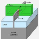
Planar CMOS processes have been offered for decades now, and all the way down through the 28nm node it has been riding the benefits of Moore’s Law. A few years back we started hearing from Intel about TriGate (aka FinFET) starting at the 22nm node as a way to use a more 3D processing approach for transistors instead of planar CMOS.… Read More
IoT Application: Road Biking Fitness
Eleven months ago I started a fitness kick in order to lose some weight, get healthy and have more energy, so I picked a familiar activity, road cycling. Being an engineer I have always loved measuring things, like my speed and distance, however I had an old-fashioned cyclocomputer called the Cateye Velo 2. This device connected … Read More
Speeding up IP and Data Management
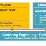
IP and Data Management (DM) for SoC teams has gradually moved from ad-hoc approaches using simple Excel spreadsheets, to home-grown software that is specific to a project or company, and finally to commercially supported tools. One such commercial toolset for IP lifecycle management is from Methodics, named ProjectIC –… Read More
DAC Update on IC Design Tools at Mentor

On Tuesday morning I headed off to the Mentorbooth at DACfor an update on their Custom IC Design and AMS Simulation/Verification tools, Christopher Cone was the presenter. Also in the room were Jay Madiraju, and Mick from Berkeley DA.… Read More
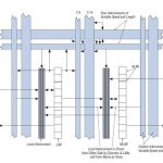
IO Design Optimization Flow for Reliability in 28nm

User group meetings are a rich source of information for IC designers because they have actual designers talking about how they used EDA tools in their methodology to achieve a goal. Engineers at STMicroelectronicspresented at a MunEDAUser Group on the topic: I/O Design Optimization Flow For Reliability In Advanced CMOS Nodes.… Read More
Making IP Reuse and SoC Integration Easier
The last graphics chip that I worked on at Intel was functionally simulated with only a tiny display size of 16×16 pixels, because that size allowed a complete regression test to be simulated overnight. Our team designed three major IP blocks: Display Processor, Graphics Processor and Bus Interface Unit. We wanted to also… Read More
Ensuring ESD Integrity
Electro Static Discharge (ESD) is a fact of life for IC designs and has been ever since electronics were first created and then started failing because of sudden, large currents flowing through the design caused by human, processing or machine contact. It’s just too expensive to layout an IC today, fabricate it, test for … Read More


Consolidation and Competition: Who is Winning the $4.5 Billion Interface IP Race?