You are currently viewing SemiWiki as a guest which gives you limited access to the site. To view blog comments and experience other SemiWiki features you must be a registered member. Registration is fast, simple, and absolutely free so please,
join our community today!
I first connected with Gerhard Angst of Concept Engineering over 15 years ago, because I was using their SpiceVision PRO tool to visual SPICE netlists received from customer designs to be debugged in a FastSPICE circuit simulator. The ability to visualize a transistor-level netlist was simply essential to quickly understanding… Read More
Four experts in the discipline of functional safety were gathered together at #56DAC in Vegas earlier in June, hosted at the Mentor booth, so I rested my legs and typed notes as fast as I could. The product areas that I first think about when functional safety (FuSa) comes up are automotive, medical and aerospace, because keeping… Read More
TSMC attends DAC every year and they do something very savvy, it’s a theatre where they invite all of their EDA and IP partners to present something of interest, followed by a drawing for a prize. At the end of the day they even have a nice prize, like a MacBook Air, which I didn’t win. On Wednesday I watched Dave Reed of Synopsys… Read More
Tuesday for lunch at #56DAC I caught up to the AI/ML experts at the panel discussion hosted by Cadence. Our moderator was the affable and knowledgable Prof. Andrew Kahng from UC San Diego. Attendance was good, and interest was quite high as measured by the number of audience questions. I learned that EDA tools that use heuristics… Read More
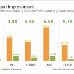
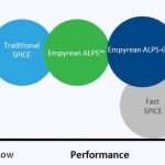
Monday afternoon at #56DAC I enjoyed attending a luncheon panel discussion from four AMS experts and moderator, Prof. Georges Gielen, KU Leuven. I follow all things SPICE and this seemed like a great place to get a front-row seat about the challenges that only a SPICE circuit simulator can address. Here’s a brief introduction… Read More
In EDA the most successful companies will often re-write their software tools in order to add new features, improve accuracy, increase capacity and of course, shorten run times. For SPICE circuit simulators we typically look at several factors to see if a new tool is worth a look or not:
- Netlist compatibility
- Model support
- Foundry
…
Read More
It’s Sunday afternoon and I just attended the annual Needham presentation at #56DAC in sunny Las Vegas, where Rich Valera shared an upbeat view of EDA and IP growth. Here are the five drivers of this growth:
- IoT
- Automotive
- Webscale/FAANGs
- AI/ML
- China
For the IoT market they’ve seen a CAGR of 8.6% to $8.2B in 2018, projected… Read More
I first started using a SPICE circuit simulator in 1978 while at Intel and have followed that market ever since then. Back at DAC in 2012 I first heard of a Chinese EDA company called IC Scape with a SPICE circuit simulator called Aeolus, so I blogged about it. Fast forward to 2019 and I heard from Ravi Ravikumar, a former co-worker from… Read More
Every morning I read the headlines from SemiWiki, CNN, LinkedIn and my Twitter feed, and it seems like every week that I read about another security breach that makes me wonder if anything online is secure. Companies try to harden their web sites, IT infrastructure and even their electronic products from being exploited or tampered… Read More
The entire history of EDA software tools has enabled engineers to design ICs and SoCs using virtual prototyping, so most of us in the industry are familiar with the idea of modeling and simulating something as complex as an IC before actually starting the manufacturing process. In a complex system like an automobile there are a lot… Read More


Beyond Moore’s Law: High NA EUV Lithography Redefines Advanced Chip Manufacturing