You are currently viewing SemiWiki as a guest which gives you limited access to the site. To view blog comments and experience other SemiWiki features you must be a registered member. Registration is fast, simple, and absolutely free so please,
join our community today!
It’s no coincidence that the TSMC Symposium is right after the Q1 earnings call. This will allow TSMC to talk more freely and they certainly will, my opinion. It is a very interesting time in the semiconductor industry and TSMC, being the bellwether, can tell us what will happen the rest of the year and give us some 2020 insights.… Read More
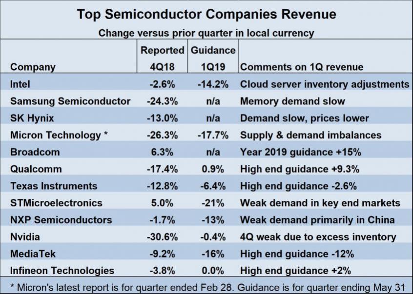
TSMC and Samsung continue to raise the competitive bar for FinFET foundry market share with dueling announcements this week. As I mentioned previously in the blog Semiconductor Foundry Landscape Update 2019, FinFETs are the market to watch with the coming onslaught of 5G and AI chips on the edge, in the cloud, and in our autonomous… Read More
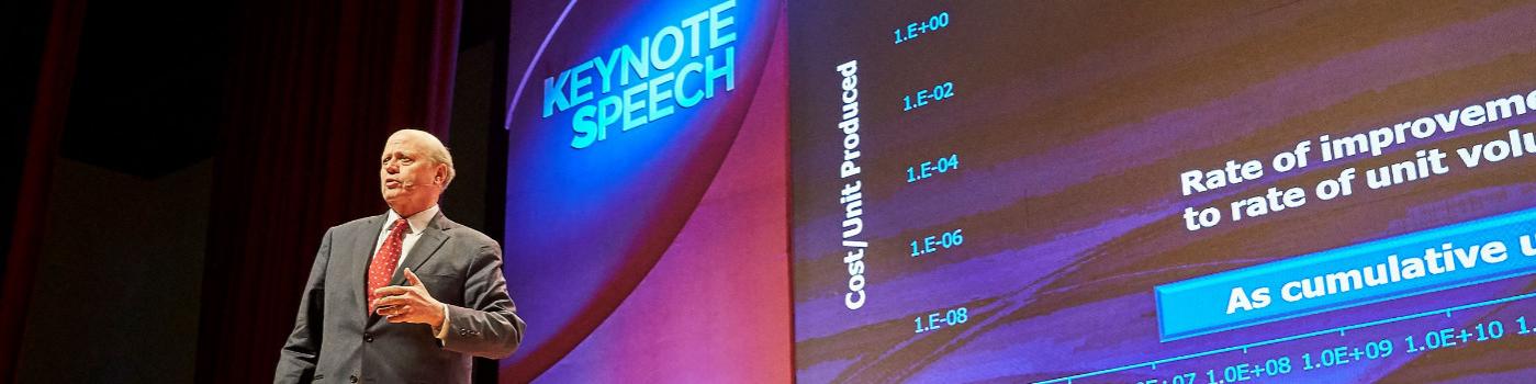
What started as blogs, or vignettes as Wally calls them, posted on SemiWiki is now a free PDF eBook. The journey starts with his school days at Stanford through 20+ years at TI and 24+ years at Mentor Graphics. Wally has traveled millions of miles meeting with every customer imaginable while presenting hundreds of different keynotes… Read More
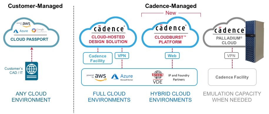
The cloud is a highly popular term that a lot of people don’t fully understand. If you are one of those people please read on as I will share my experience, observations, and opinions. Even if you are a cloud aficionado you may want to catch up on what’s new with EDA cloud services so again read on.
When we first started SemiWiki 9 years … Read More
In 2015 Intel acquired Altera for $16.7B changing one of the most heated rivalries (Xilinx vs Altera) the fabless semiconductor ecosystem has ever seen. Prior to the acquisition the FPGA market was fairly evenly split between Xilinx and Altera with Lattice and Actel playing to market niches in the shadows. There were also two FPGA… Read More
The semiconductor foundry landscape changed in 2018 when GLOBALFOUNDRIES and Intel paused their leading edge foundry efforts. Intel quietly told partners they would no longer pursue the foundry business and GF publicly shut down their 7nm process development and pivoted towards existing process nodes while trimming headcount… Read More
Every system-on-chip (SoC) designer worries about power. Many widely used electronics applications run on batteries, including smartphones, tablets, autonomous vehicles, and many Internet-of-Things (IoT) devices. Even “big iron” products such as network switches and compute servers must be careful when it comes to power… Read More
What does Qualcomm, Intel, and Facebook have in common? Well, for one thing they all bought network onchip communications (NoC) IP companies. As I have mentioned before, semiconductor IP is the foundation of the fabless semiconductor ecosystem and I believe this trend of acquisitions will continue. So, if you are going to start… Read More
There was an interesting keynote at DVCon last month. It was titled “Thriving in the Age of Digitalization” which introduced the concept of digital twins for design and production. It was presented by Fram Akiki who is a relative newcomer to EDA but has an interesting history so I will start there.
Fram and I got started in the semiconductor… Read More
I had a chat with Bob Smith, Executive Director of ESD Alliance, about the upcoming SEMI conference in China. More than 100,000 people are expected to attend which is beyond my comprehension. SEMICON in San Francisco is maybe 20,000 people which is the largest conference I attend. I’m not sure if the Design Automation Conference… Read More


Intel, Musk, and the Tweet That Launched a 1000 Ships on a Becalmed Sea