The foundry model, multi-source IP blocks, advanced packaging technologies, cloud computing, hyper-connectivity and access to open-source software have all contributed to the incredible electronics products of recent times. Along with this, the complexity of developing and taking a chip to market has also increased. And that is just from the effort perspective to implement a chip that performs to its specification. Add to this, the competitive market forces that demand faster time to market cycles.
While companies overcome these challenges by leveraging a combination of top-notch talent, tools, processes and proprietary methodologies, a new generation of chips are taking these challenges to a higher level. Artificial Intelligence (AI) driven applications such as security, visual cognition, and natural language comprehension/processing are behind the demand for these AI chips. Are time-proven techniques of overcoming time to market challenges sufficient when dealing with these AI chips? This is the backdrop for a whitepaper authored by Richard Oxland and Greg Arnot, both from Siemens EDA.
The whitepaper describes how new tools and methodologies may be required to help designers optimize hardware and software not only during the development phase but also after the chips are deployed in the field. It establishes that designers having intimate visibility into the operation of the chip is imperative for the on-time development of these AI chips. It explains how analytics capabilities embedded within these chips not only can help take a chip to market faster but also assist with optimizing the performance of the systems. This blog covers the salient points I gleaned from the whitepaper.
As embedded electronic systems get more complex, the interaction between hardware and software also becomes more complex. This makes debugging and optimizing for performance a very challenging and extremely time-consuming endeavor. Not only must root causes of bugs be determined and corrected but sub-optimal performance of a correctly functioning system must also be resolved under severe time-to-market pressures.
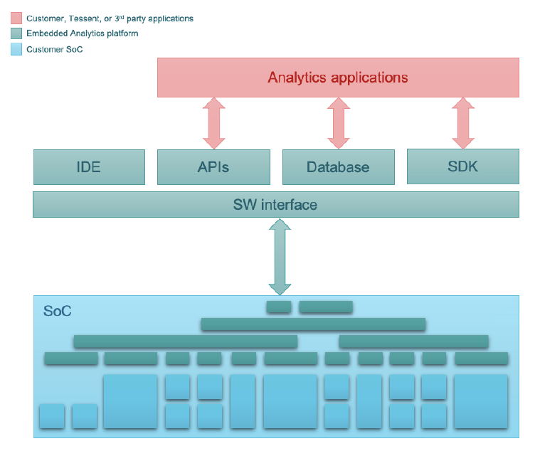
The authors discuss the Tessent Embedded Analytics platform and use an AI accelerator chip as an example to showcase the value product developers stand to gain from utilizing embedded analytics. The Tessent Embedded Analytics architecture has been designed and the platform implemented from the bottom up as a scalable, flexible and powerful solution to harness complexity in SoCs and embedded systems. The platform comprises a portfolio of silicon IP and software interface, together with APIs, an SDK, and database and IDE functionality. Refer to figure below.
Figure: Tessent Embedded Analytics Architecture
 Source: Siemens EDA
The analytics platform combines IP and software designed to provide functional insights into complex SoC behavior. Tessent silicon IP can monitor internal bus transactions, processor execution, and other system-level activity within the device, correlated across the system, and at the right level of detail for the task in hand. The platform also contains the SW tools, APIs, and libraries required to process functional data and give designers a detailed understanding of the behavior of the hardware and software in the embedded system.
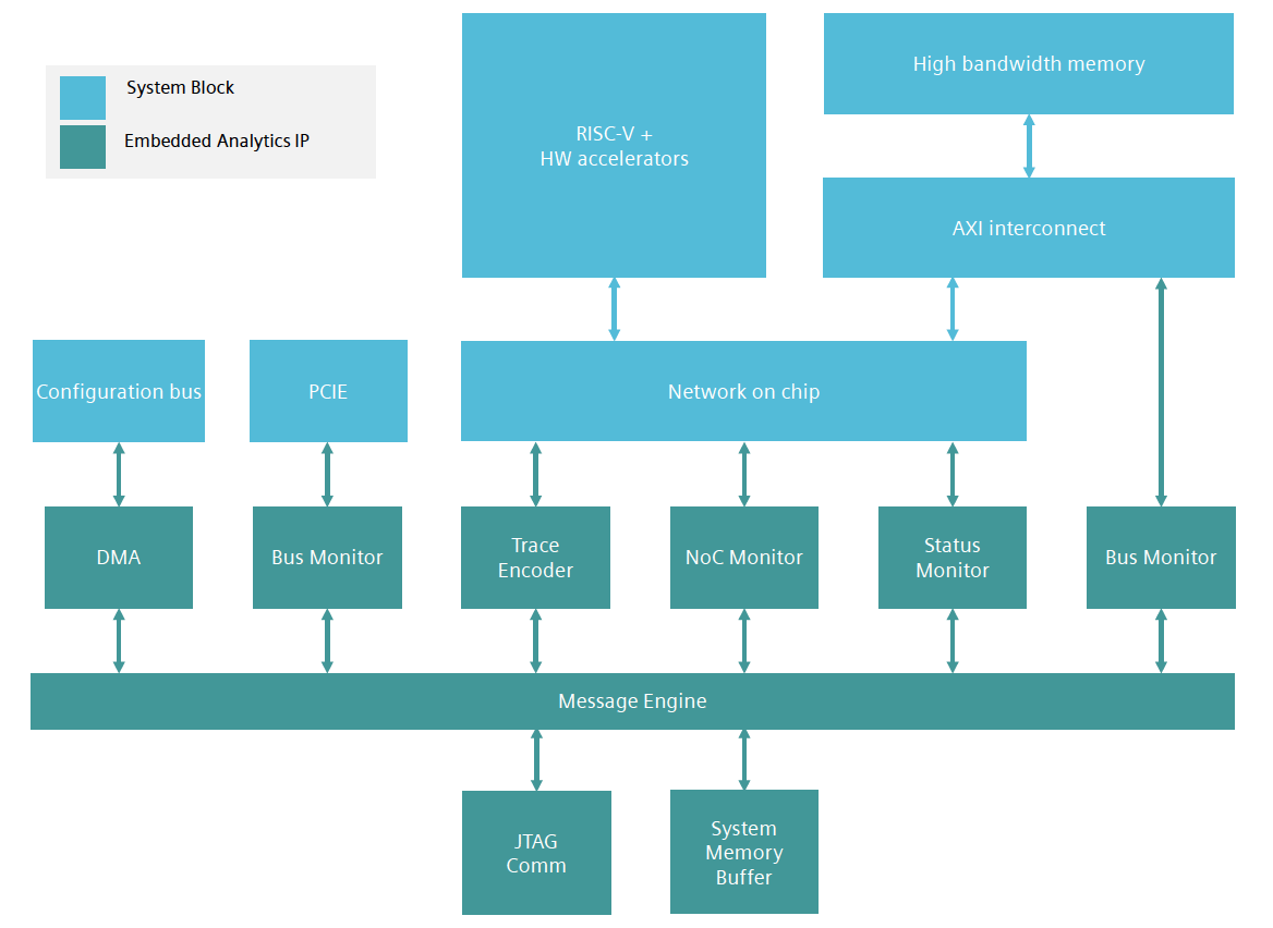
The whitepaper goes into details of how different embedded analytics modules bring value to the chip development process. Refer to figure below for the different analytics modules used with the AI accelerator chip. You can learn about all available embedded analytics modules by downloading the Tessent Embedded Analytics Product Guide.
Figure: Tessent Embedded Analytics Modules in an AI Accelerator Chip

Source: Siemens EDA
System Validation and Optimization
The customers for this example AI accelerator chip are Machine Learning (ML) application developers. Their software must be able to take advantage of all the unique hardware capabilities of the accelerator chip and maximize performance. As the limiting factor for system performance is the data throughput between memory and functional units, the chip design team must be able to optimize the high-bandwidth-memory (HBM) controller and memory banking schemes with confidence.
Assuming that memory corruption events are observed during the system validation phase, the team would have traditionally looked to simulation for debugging the issue. But as the use case is large, as in the case with many AI chips, debugging this way could consume many days or even weeks. This is where embedded analytics comes in as the savior. Using the supplied Python API and library of tests, the validation team configures the embedded analytics subsystem to find the root cause of the memory corruption. The DMA module is used to write to and examine the contents of the HBM in a precisely determined timeframe. The Bus Monitor is set up to look for transactions within a fixed address range and capture bus trace into a circular buffer. And the Enhanced Trace Encoder provides a mechanism to monitor the program execution of the relevant CPU.
With the memory corruption issue resolved, engineers can now focus on measuring response latencies of the HBM for different banking schemes using the built-in functionality of the Bus Monitor and the Python API. This mechanism allows for quick and easy experimentation with different hardware configurations.
Optimization in the Field
After system validation and optimization, a chip vendor may learn during field trials that the customers’ own applications may not be meeting expected performances. Fortunately, the same embedded analytics used during system validation can be leveraged to optimize memory bandwidth and latency.
Summary
The Tessent Embedded Analytics platform provides a solution that not only helps with the debug of an AI SoC during its development phase but also performance optimization of the product throughout its lifecycle. For full details, you can download the whitepaper here.
Also Read:
AMS IC Designers need Full Tool Flows
Symmetry Requirements Becoming More Important and Challenging
Debugging Embedded Software on Veloce
Share this post via:


Comments
There are no comments yet.
You must register or log in to view/post comments.