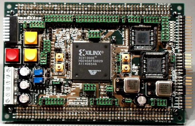
 Verifying chip designs has always suffered from a two-pronged problem. The first problem is that actually building silicon is too expensive and too slow to use as a verification tool (when it happens, it is not a good thing and is called a “re-spin”). The second problem is that simulation is, and has always been, too slow.
When Xilinx and Altera produced field-programmable gate-arrays (FPGAs), which were reprogrammable, it didn’t take long for ASIC designers to realize that these could be a third prong to solve their verification problem. Much cheaper than building silicon but much faster than simulation.
There were no commercial solutions at first for FPGA prototyping. Everyone who wanted to do it had to buy FPGAs (or an FPGA-based board) and then cobble together a flow that worked. The biggest issue was probably that the types of designs for which this would be an interesting approach had more gates than the largest FPGAs, so the designs had to be partitioned. But partitioning a typical design meant that more signals needed to go between the various partitions then were actually available on the FPGAs, so the pins needed to be multiplexed. This is a problem that continually gets worse since, to a first approximation, the number of gates grows quadratically and the number of pins linearly meaning that there are thousands of gates per pin. So it was clearly not a straightforward approach, and it required a lot of knowledge about the design to get it ready, and a lot of knowledge about FPGAs and FPGA tool flows to actually get anything to work.
Like most things where lots of customers are making something difficult independently, some people saw an opportunity to create a commercial product to serve the whole market. I expect there were other companies lost in the mists of pre-internet days but one company survives from that era to the present day.
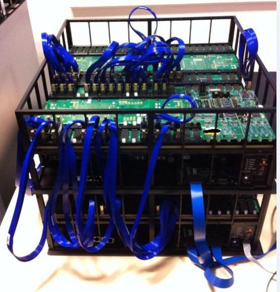 In 1987 Hardi Electronics was formed in Sweden. In 2000, they created an FPGA prototyping system called HAPS. As described by Hardi:HAPS is a modular, high performance and high capacity FPGA-based system for ASIC prototyping. HAPS comprises multi-FPGA motherboards and standard or custom-made daughter boards which can be combined in a wide variety of ways in order to quickly assemble ASIC prototyping systems. Rapid assembly is facilitated by the availability of many standard daughter boards including video processing, memory and interfaces to Ethernet, USB, PCI Express and ARM core modules. Customers prefer the time-to-market advantage of using an off-the-shelf prototyping solution, which can save months in the critical verification phase.
In 2007 Synplicity acquired Hardi Electronics for $24M. At the time, Synplicity was one of two companies that competed in the merchant FPGA synthesis market, competing with the free (or nearly free) solutions provided by the FPGA vendors, Mentor being the other. But Synplicity was not long as an independent company and Synopsys acquired them in 2008 for $227M. HAPS has been through several generations, the most recent of which, HAPS-80, was announced just last week.
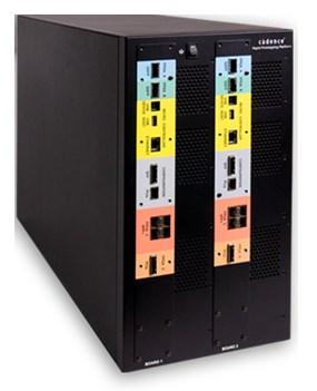 In the meantime, Cadence also decided to create an FPGA prototyping solution. The first generation, imaginatively named Rapid Prototyping Platform, came out in 2011. By the second generation it had a real name. In 2014 Cadence announced their second generation of the product called Protium.
In 2003, another company, S2C, was founded in Silicon Valley to address the FPGA prototyping market. They have grown and have several hundred systems installed. Developing and manufacturing is in China and Taiwan respectively.
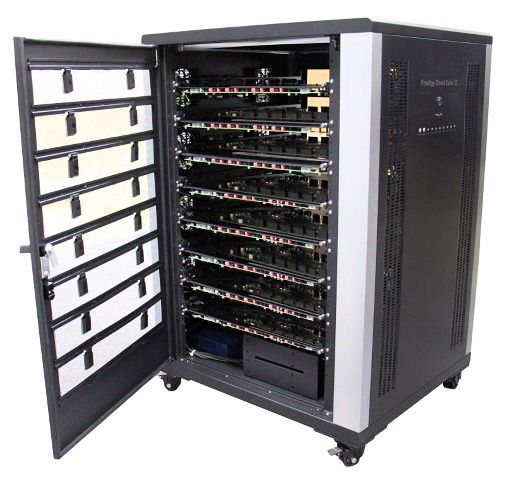 So that is the scene today. About half the market is still people putting together their own prototyping systems and there are three suppliers with off-the-shelf product portfolios: Synopsys, Cadence and S2C. All the solutions consist of two parts. There is a hardware component, which consists of the range of boards and connectors. And there is a software component which takes the design, partitions it, handles the multiplexed signal connectivity between the arrays, creates the bitstreams to program them, and provides access and visibility to debug the design.
FPGA prototyping can be used by chip designers to give them a way to run huge amounts of verification vectors, often including booting an operating system and bringing up drivers. It can also be used by software designers who need something on which to run their software before silicon is available. Even when silicon is available, the FPGA prototyping system often provides a better environment for debugging the code.
Share this post via:


Speculative Execution: Rethinking the Approach to CPU Scheduling