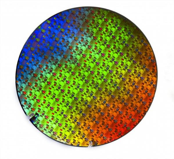
It was a pleasure to see the GlobalFoundries (GFI) corporate pitch at the Mentor Graphics U2U Conference last week. Wally Rhines is a tough act to follow but Mojy Chian, Senior Vice President of Design Enablement at GlobalFoundries, presented a compelling argument for a refined foundry business model. The GFI people were also nice enough to send the presentation, offer a private briefing, and honor my request for a picture of an actual 28nm test chip wafer.
I first met Mojy Chian at Conexant and again at Altera where he was Vice President of Technology managing development, infrastructure, and manufacturing (down to TSMC 40nm). I last met Mojy at lunch on St Patrick’s day. When I heard Mojy joined GlobalFoundries I knew they were absolutely serious about the business side of semiconductor design and manufacturing.
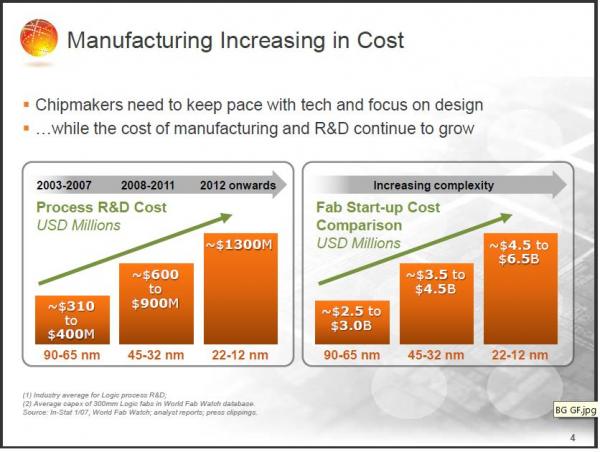
Clearly the fabless model continues to thrive at 40nm and below. Due to the cost, only a handful of semiconductor manufacturers will develop 28nm process technology. Due to the cost, only the top fabless companies will design at 28nm, so the competition for their business will be fierce. The challenge for GlobalFoundries is to differentiate from Taiwan and that was the underlying message in this presentation: “GlobalFoundries is everything TSMC is not”.
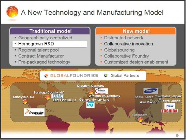
Point #1 is the basis for their name, being global and not putting your semiconductor manufacturing eggs in one regional (Taiwan) basket. TSMC’s Morris Chang responded directly to this “Global Semiconductor Company” challenge by saying that TSMC will stay in Taiwan. The major reason being the economies of scale. According to Chang, TSMC only needs to run its Taiwan wafer fabrication plants at 40% capacity to break even, compared with 80% for “global” rivals.
The Chartered Semiconductor Common Platform marketing initiative will continue under GFI. In theory, the process development is collaborative and the cost is shared amongst the members. Common Platform clearly did not work for the now defunct Chartered Semiconductor which in my opinion was an implementation problem. If GFI drives this alliance hard it will work, believe it.
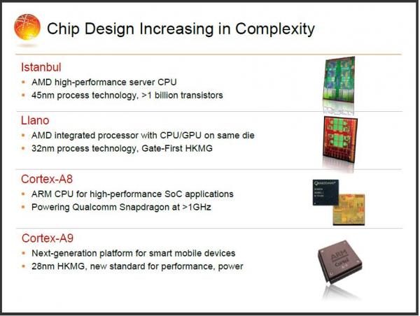
Point #2 is technology and the differing versions of HKMG technology. David Lammers did an excellent write-up: Gate First or Gate Last: Technologists Debate High-k . The bottom line is that Intel and TSMC will do Gate-Last. GFI, IBM, and other Common Platform Alliance members will do Gate-First. From what I have learned, Gate-Last will favor high performance and high yield designs but will require restricted design rules (RDRs). Gate-First will favor low power and smaller die sizes but may not scale past 22nm. I see this as a major battle ground for the foundry business. My opinion, whoever wins the 28nm node will lead the foundry business for the next decade.
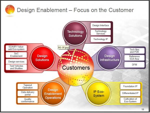
Point #3 is semiconductor design enablement or the EDA, IP, and Design Services ecosystem. GlobalFoundries has Common Platform, TSMC has the Open Innovation Platform. One thing that has changed with Common Platform is that GFI is providing generous financial incentives for partners and we are talking about millions of dollars in life lines to companies that have struggled for profitability. GFI also pledged not to compete with partners, which is a direct shot at TSMC who has spent 100’s of millions of dollars developing proprietary design enablement technology.
Speaking of TSMC design enablement, the annual TSMC 2010 Technology Symposiums start next week in San Jose with Morris Chang as keynote speaker. TSMC has scheduled an in-person briefing for me with Shang Yi Chiang, senior vice president of R&D, to discuss 28nm technology so next week’s blog will be a follow-up to this.
Share this post via:


The Intel Common Platform Foundry Alliance