Intel, long a leader in semiconductor manufacturing, is on a determined journey to reclaim its technological leadership in the industry. After facing significant challenges in recent years, the company is making a concerted effort to adapt and innovate, with a clear focus on AI-driven technologies, advanced packaging solutions, and building a robust ecosystem.
During last week’s Intel Foundry Direct Connect event, Intel outlined its strategy and the investments it is making to enable this transformation. The company certainly does not intend to be encumbered by its recent history.

Transforming Intel Foundry: A Customer-Centric Approach
Intel is undertaking a significant transformation of its foundry business, with a renewed focus on becoming a customer-first, service-oriented organization. At the core of this strategy is a commitment to close collaboration with customers to ensure Intel not only meets, but anticipates their evolving needs. This transformation is guided by three strategic priorities:
Matching Technology to Customer Needs: Intel is aligning its technology offerings with the specific demands of industries like artificial intelligence (AI) and high-performance computing (HPC). Flexibility, predictability, and scalability are key pillars of this approach.
Improving Execution and Responsiveness: The company is refining its internal processes to better deliver on time and meet customer expectations with greater reliability.
Expanding the Ecosystem: Intel is investing significantly in ecosystem growth, including design enablement, IP support, and advanced packaging. These investments are designed to support its foundry business at scale.
Through these efforts, Intel aims to reshape its foundry operations into a comprehensive, end-to-end solutions provider equipped to meet the complex requirements of the modern semiconductor industry.
AI and Advanced Packaging: The Next Frontier
AI is transforming semiconductor design and manufacturing, and Intel is positioning itself as a foundational technology provider for this revolution. Recognizing that future computing performance relies not just on smaller transistors but also on smarter integration, Intel is making bold moves in advanced packaging.
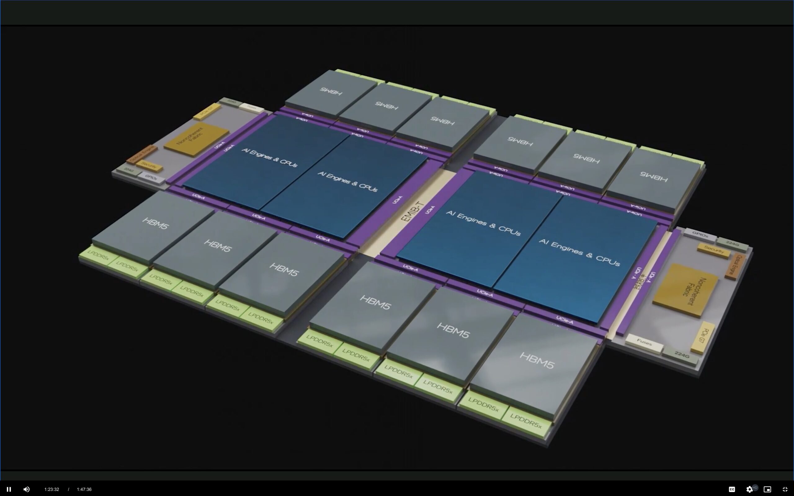
Intel’s packaging technologies, including 2.5D and 3D solutions, are designed to offer increased design flexibility, faster time-to-market, and efficient performance scaling. Technologies such as Through-Silicon Vias (TSVs), embedded silicon bridges (E-bridges), and interconnect standards like UCIe are being implemented to address the demands of AI workloads—high bandwidth, low latency, and energy efficiency.
Intel’s EMIB (Embedded Multi-die Interconnect Bridge) enables high-density die-to-die connections in a 2.5D package without the need for a silicon interposer, offering cost and performance benefits for large chiplet-based designs. Foveros, Intel’s 3D stacking technology, allows different logic tiles to be stacked vertically, enabling heterogenous integration across process nodes. Foveros Direct, an evolution of this platform, introduces direct copper-to-copper bonding for ultra-high-density, low-resistance interconnects, pushing the boundaries of integration and energy efficiency.
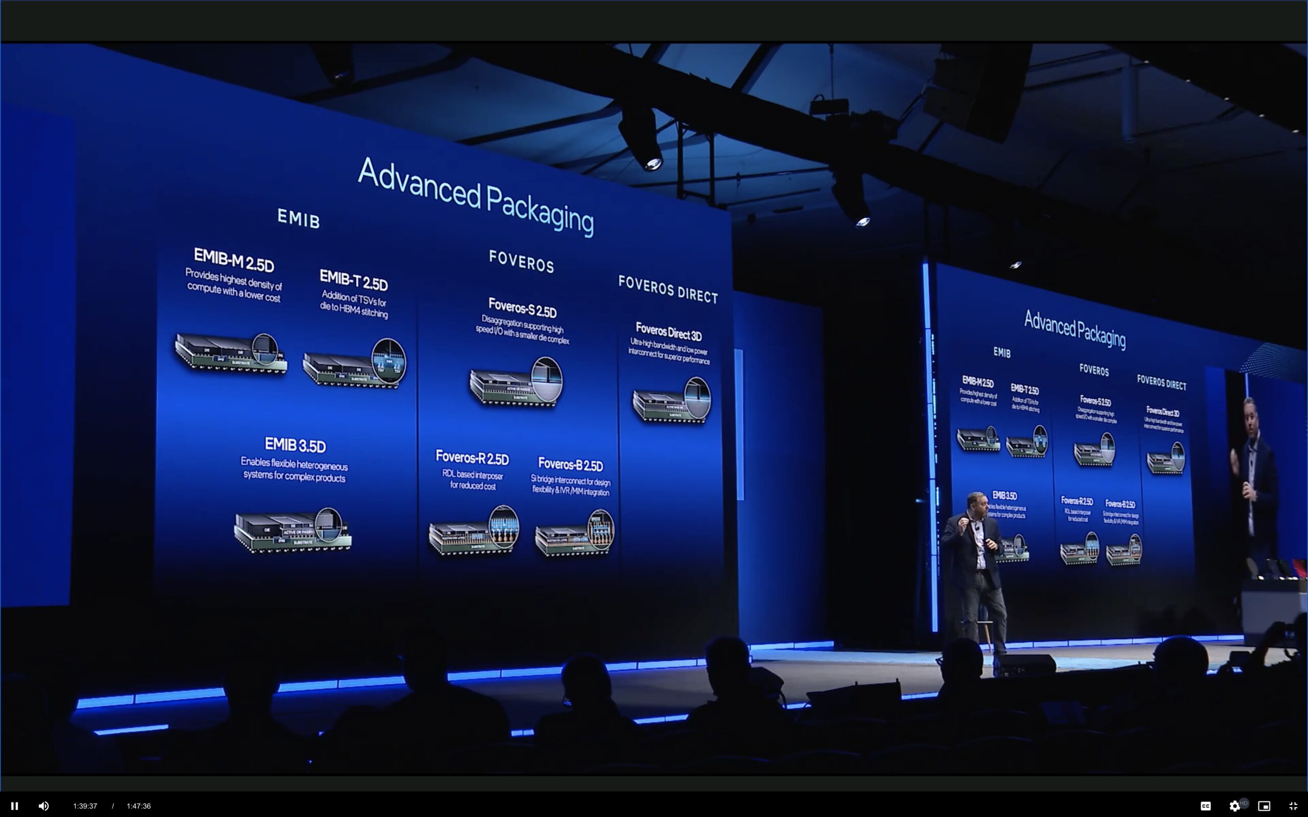
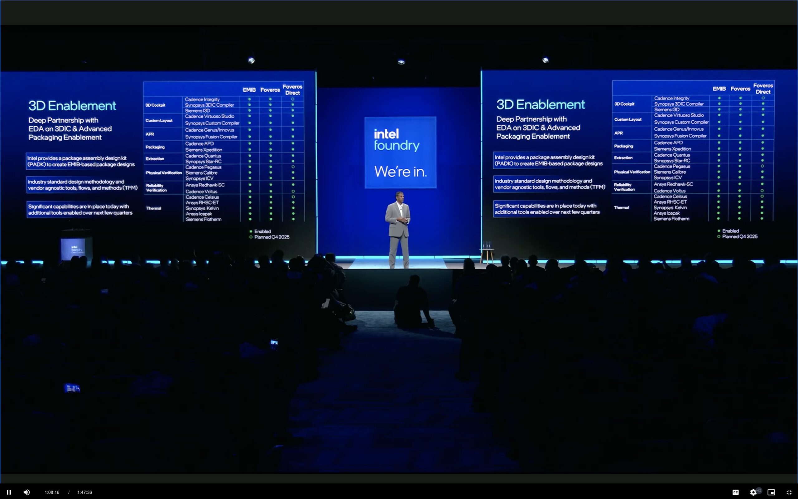
The development of advanced solutions like HPM4 for high-performance memory and support for reticle-size packages up to 12X the standard, enable Intel to support large, AI-centric designs at scale.
A Collaborative Ecosystem: Strengthening Partnerships
Intel recognizes that its comeback won’t happen in isolation. Key to its strategy is building a robust, collaborative ecosystem. Lip-Bu Tan, CEO of Intel, underscored this during his talk, emphasizing the importance of ecosystem enablement to support AI’s massive growth.
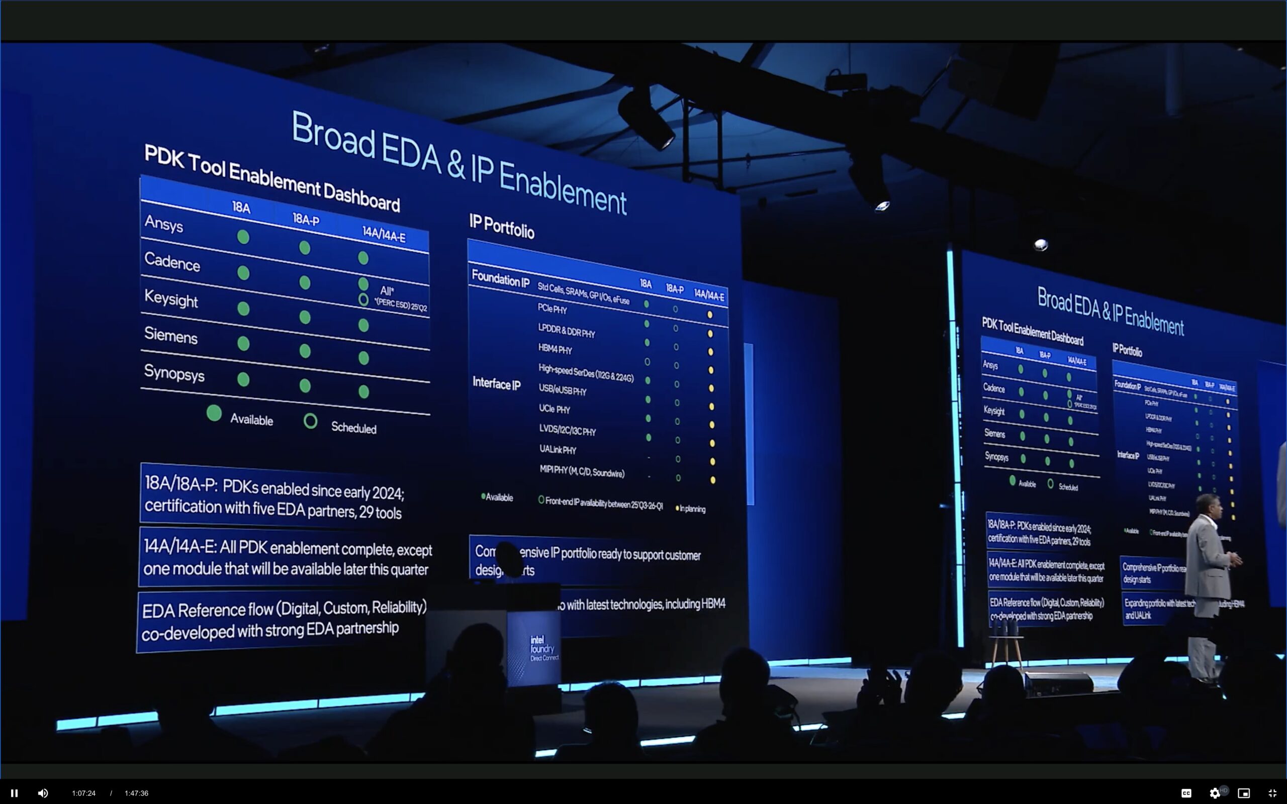
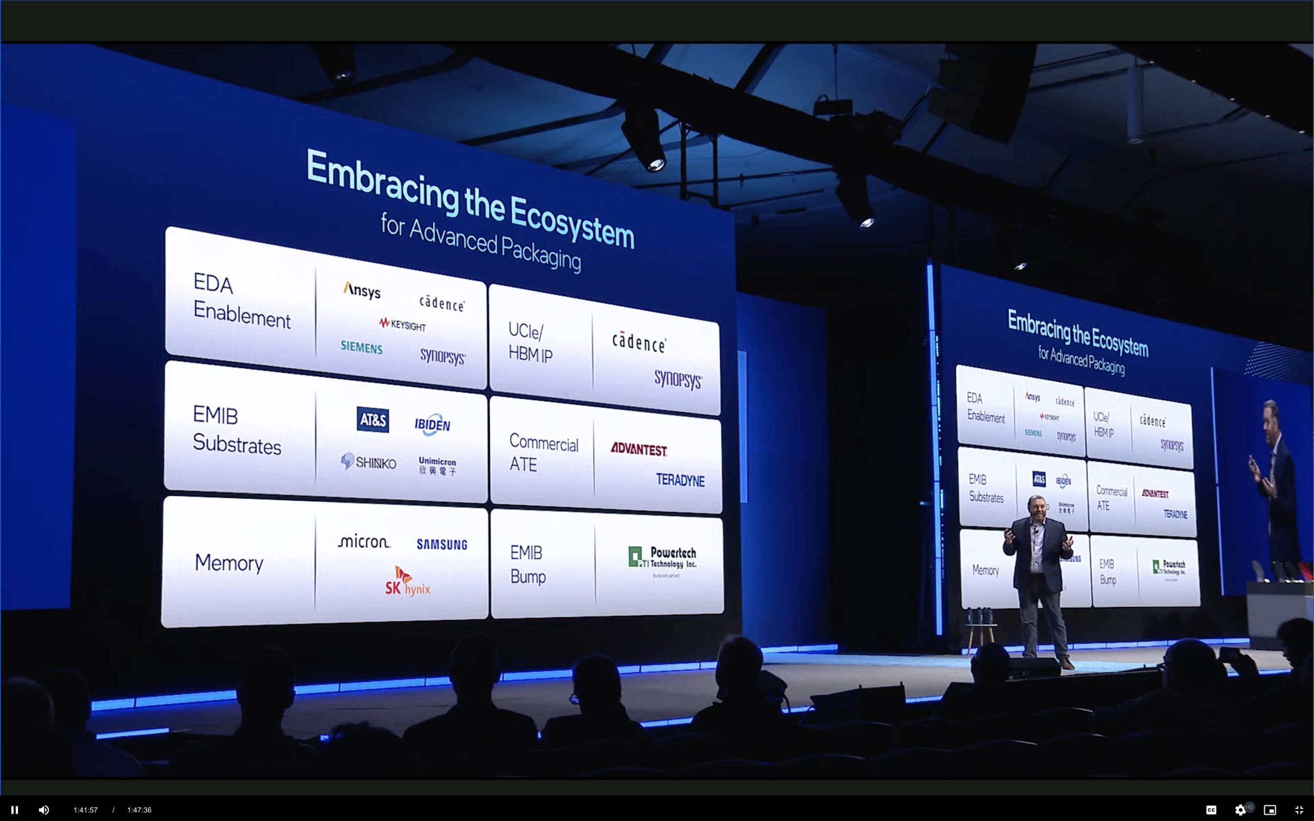
Its leadership in forming the Chiplet Alliance, comprising over a dozen companies, highlights its effort to create a secure, standardized, and interoperable chiplet ecosystem. This initiative underlines Intel’s commitment to building a connected value chain across design, packaging, and manufacturing.
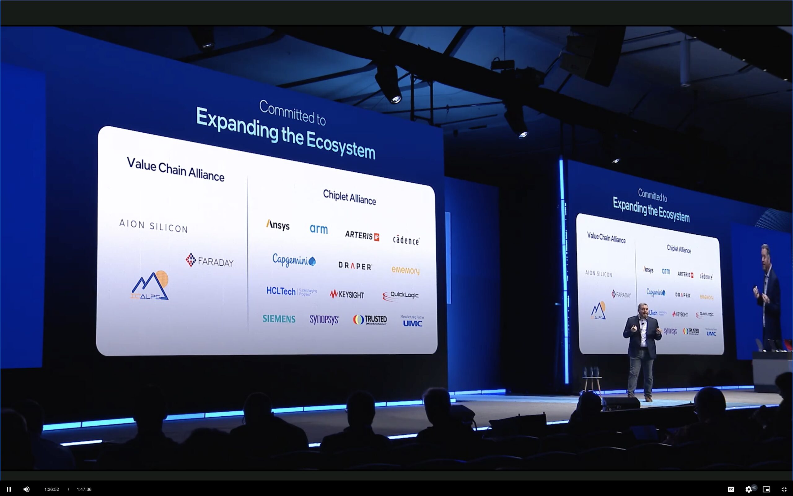
Intel is also partnering with United Microelectronics Corporation (UMC) to bring its 12nm technology to market, aimed at serving specialty applications. This collaboration leverages Intel’s manufacturing expertise with UMC’s strengths in design enablement. You can read about this on a separate post on SemiWiki: Intel’s Foundry Transformation: Technology, Culture, and Collaboration
The U.S. Government’s Role in Intel’s Vision
Intel views the U.S. government as a foundational partner in its mission to bring semiconductor leadership back to American soil. Programs like RAMP (Rapid Assured Microelectronics Prototyping) and the Secure Enclave Program are key enablers of trusted domestic manufacturing. These initiatives support the development and ramp-up of Intel’s cutting-edge 18A and 16 nodes, all of which will be manufactured in the U.S. Intel’s alignment with national security and economic priorities strengthens its position as both a commercial and strategic partner.
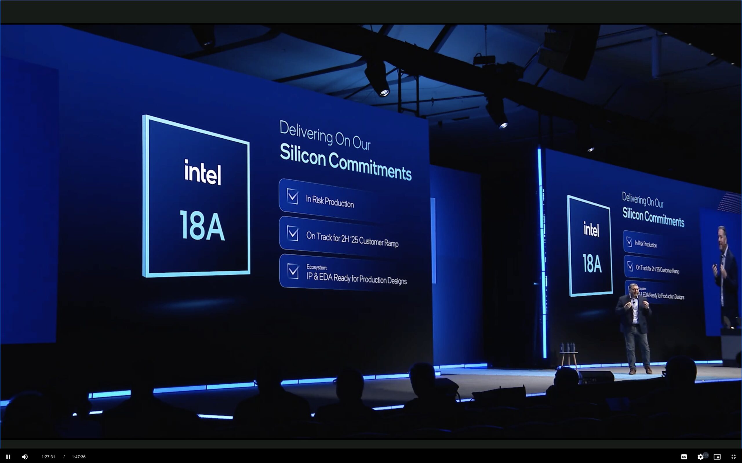
The government’s involvement is not just about funding—it’s about ensuring a resilient and secure semiconductor supply chain for both public and private sectors.
Summary
Intel’s strategy to regain technological leadership is built on four pillars: advanced process technology, next-generation packaging, ecosystem collaboration, and strong public-private partnerships. Looking ahead, Intel’s roadmap is anchored in technologies that provide scalable performance with predictable delivery.
With a customer-first mindset, a reinvigorated focus on execution, and a bold investment in innovation, Intel is poised to lead the next era of semiconductor technology.
Also Read:
Intel’s Path to Technological Leadership: Transforming Foundry Services and Embracing AI
Intel Presents the Final Frontier of Transistor Architecture at IEDM
Share this post via:


Comments
5 Replies to “Intel’s Path to Technological Leadership: Transforming Foundry Services and Embracing AI”
You must register or log in to view/post comments.