




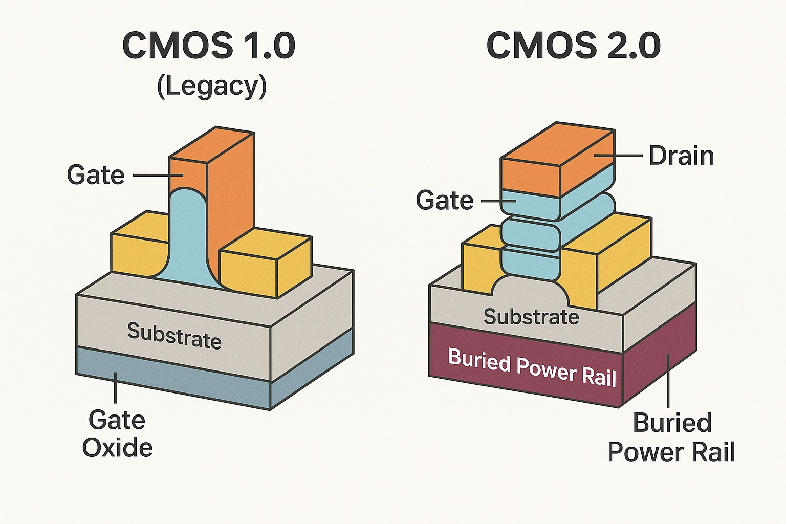


CMOS 2.0 refers to the next era of transistor and process technology innovation that succeeds traditional FinFET-based CMOS scaling. It encompasses a suite of architectural, materials, and integration innovations aimed at extending Moore’s Law into the angstrom era. CMOS 2.0 is characterized by Gate-All-Around (GAA) transistors, Complementary FETs (CFET), backside power delivery, buried power rails, and 3D monolithic integration.
While not a formal standard, the term is widely used in research and industry to define the paradigm shift underway in sub-3nm process nodes. It is a philosophy of holistic scaling that combines device, interconnect, and packaging innovations to overcome power, performance, and area (PPA) limitations.
Key Technologies in CMOS 2.0
1. GAAFET (Gate-All-Around FET)
-
Channels are surrounded on all sides by the gate, enhancing electrostatic control and reducing leakage.
-
Introduced commercially by Samsung at 3nm (SF3E), used in TSMC N2 and Intel 20A/18A (RibbonFET).
2. CFET (Complementary FET)
-
Vertically stacks nFET and pFET for greater area efficiency.
-
Expected post-GAAFET (Intel 14A, TSMC A14), likely by ~2027–2028.
3. Backside Power Delivery (BSPDN)
-
Moves power rails below the transistor layer via wafer thinning and through-silicon vias.
-
Reduces IR drop and congestion on the frontside.
-
Pioneered in Intel’s PowerVia technology.
4. Buried Power Rails (BPR)
-
Embeds power rails into the substrate below the transistors.
-
Enables tighter cell height and efficient power delivery.
5. Monolithic 3D IC and Advanced Packaging
-
Die stacking with direct interconnects (e.g., hybrid bonding).
-
Examples: Intel Foveros, TSMC SoIC, Samsung X-Cube.
Timeline of CMOS 2.0 Milestones
| Year | Milestone |
|---|---|
| 2011 | FinFET production begins (Intel 22nm) — peak CMOS 1.0 |
| 2018 | IBM demonstrates CFET stacking in research |
| 2021 | Intel announces RibbonFET + PowerVia (20A, 18A roadmap) |
| 2022 | Samsung SF3E enters early production with GAAFET |
| 2024 | TSMC N2 in risk production using nanosheet GAAFET |
| 2025 | Intel 18A (GAAFET + BSPDN) enters production |
| 2026–2027 | Intel 14A and TSMC A14 to adopt CFET and deeper CMOS 2.0 elements |
Industry Drivers
-
Moore’s Law: Extending transistor scaling and density into sub-2nm nodes.
-
AI & HPC: Need for higher performance-per-watt and interconnect efficiency.
-
Mobile/Edge: Ultra-low power with performance bursts.
-
Chiplet & 3D Integration: Enabling fine-grained disaggregation of IP blocks.
Major Industry Players
-
Intel: RibbonFET (GAAFET), PowerVia (BSPDN), 18A & 14A roadmap.
-
TSMC: N2 with GAAFET, BPR/BSPDN, advanced CoWos/SoIC packaging.
-
Samsung: MBCFET™, SF2/SF1.4 roadmap, backside power delivery.
-
IBM: Pioneering CFET and nanosheet research.
-
IMEC: Roadmapping and R&D in CFET, 2D materials, and BSPDN.
Notable Quotes on CMOS 2.0
“We’re entering the Angstrom era — a new phase where innovation in power delivery, transistor structure, and 3D stacking defines progress, not just shrink.”
— Pat Gelsinger, CEO of Intel
“Gate-All-Around transistors give us the electrostatic control needed for future scaling, but the real gains come when we integrate backside power delivery and chip stacking.”
— Dr. Kevin Zhang, SVP of Technology Development, TSMC
“With CMOS 2.0, you are no longer just shrinking; you’re reshaping the silicon stack — from buried power rails to vertically stacked transistors.”
— Luc Van den hove, CEO of imec
“CFET is perhaps the most radical change in transistor architecture since the MOSFET — stacking nFET and pFET requires atomic precision and complete EDA retooling.”
— Dr. Mukesh Khare, IBM Research
“PowerVia is not just about power routing — it’s about opening up the frontside for signal integrity and pushing CMOS design beyond 2nm.”
— Ruth Brain, Intel Fellow
Outlook
CMOS 2.0 is not a single technology but a framework of innovations enabling continued semiconductor scaling into the 2030s. It will play a foundational role in AI, HPC, edge computing, and future quantum-augmented processors. As transistor scaling slows, CMOS 2.0 also tightly couples with advanced packaging and system-level co-design, ushering in a new era of More than Moore.
Also Read:
3D IC (Three-Dimensional Integrated Circuit) Wiki
TSMC Wiki
imec Wiki
Share this post via:










The silent killer of analog reliability: Why SPICE misses floating net