
The upcoming Keysight EDA 2025 launch has three familiar tracks: RF circuit design, high-speed digital circuit design, and device modeling and characterization. However, this update features a common thread between the tracks – AI-enhanced design workflows. AI speeds modeling and simulation, opening co-optimization for complex designs. It also gives design teams more freedom to incorporate Keysight EDA tools into their workflows with Python customization. Here is a preview of what designers can expect, including some short videos on each of the three tracks, with more details to come in a multi-region, multi-track live and archived webinar event.
RF circuit designers move into a 3DHI co-design cockpit
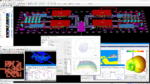
Keysight Advanced Design System (ADS) is unmatched as the state-of-the-art platform for RF design and multi-domain co-simulation. Python scripting features already in ADS provide the capability for automating tasks and customizing the user interface. However, RF design complexity continues to grow, typified by the emergence of 3D heterogeneous integration (3DHI) techniques with dense multi-technology packaging.
Rising complexity creates a pressing need to insert RF designs into appropriate system contexts for simulation. However, workflows cannot tolerate the potential of spiraling simulation run times for comprehensive, realistic evaluations with more data points and swept parameters, which could force users to limit how frequently crucial RF simulations execute. Leaving unpredictable real-world effects undetected until physical prototypes is a poor choice.
Fortunately, it’s a choice ADS users won’t face. The previous phase of Keysight EDA research concentrated on broadening the analysis types in ADS, unifying measurement science with Keysight’s test and measurement instrumentation, and speeding simulations with innovative algorithms such as compact test signals, fast envelope techniques, and distortion EVM.
This new phase in Keysight EDA 2025 re-engineers the core simulation platform in ADS to provide external programmatic simulation control through an application programming interface (API), including Jupyter Notebook support. The API also enables new levels of Python customization, including user interfaces, importing layout or modeling data for simulation, creating visualizations for simulation results, and training artificial neural network (ANN) models. The newly re-engineered core delivers as much as 6x improvement in simulation times.
The result transforms ADS into a co-design cockpit where teams can efficiently manage multi-domain RF design and simulation in one open environment. This cockpit minimizes design manipulation while enabling comprehensive, accurate simulation as often as desired earlier in workflows. It also prepares ADS for future growth in RF design complexity and AI-driven command invocation. Floating license packs can set up multiple users for parallel basic analyses, a power user for high-performance specialized analysis, or any combination that makes sense for a design workflow.
High-speed digital circuit design gets enhanced crosstalk analysis
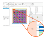
One of the most prominent 3DHI techniques is chiplets, with many teams interested in or pursuing designs based on the Universal Chiplet Interconnect Express (UCIe) specification. UCIe seeks to create an ecosystem where chiplets from different technology nodes can interoperate within a single package, and ongoing enhancements to the specification target optimized die-to-die signaling, improving performance.
Signal integrity is the biggest issue in achieving reliable UCIe designs. As interconnect speeds increase, signal integrity concerns are growing. Teams must carefully analyze UCIe designs, examining all metrics simultaneously to avoid the pitfall of optimizing one metric at the expense of degrading others. To make a comprehensive die-to-die interconnect layout and analysis possible, Keysight created Chiplet PHY Designer, an extension to ADS that provides UCIe simulation and enhanced analysis of the voltage transfer function (VTF) and forward clocking.
In the EDA 2025 update, one Keysight focus for chiplets is enhanced support for quarter data rate (QDR) clocking. Approved as an addition to the UCIe 2.0 specification in August 2024, QDR provides a path to lower UCIe clock rates, reducing design risk while still offering high-performance data transfer rates. Simulating QDR in ADS essentially repeats PHY analysis four times, once for each clock phase. AI enters the equation to help Chiplet PHY Designer visualize VTF crosstalk and VTF loss masks for different data rates and automatically model and optimize link design parameters for best results.
Device model re-centering improves speed by an order of magnitude
Creating process design kits (PDKs) for advanced semiconductors such as III-V technology can be tedious. Engineers try to fit a basic set of measurements into an existing model for a previous device in what is known as model re-centering. However, the fit is often less than ideal and may only work for a tightly bounded set of operating conditions, such as bias voltages or frequency ranges. If the application context changes, a new set of exhaustive measurements could take months. Without more measurement data, partially re-centered models can lack fidelity, leading to inaccurate simulation results.
Model re-centering fidelity is imperative with devices applied in more complex designs for wireless standards featuring higher-order modulation and broader bandwidths. Too much of a difference between simulations and measurements under parameter sweeps manifests as a significant risk of prototype failure.
The EDA 2025 update includes a refresh of Keysight IC-CAP with its ANN Toolkit leveraging AI to quickly re-center models spanning more parameters without exhaustive measurements, reducing the model re-centering process to hours instead of weeks and lowering the expertise required to obtain accurate modeling results.
Learn more at the Keysight EDA 2025 launch event
These are just some of the capabilities in Keysight EDA 2025. It’s also important to note that many EDA 2025 RF circuit design discussions apply to Cadence, Siemens, and Synopsys design platform users considering Keysight RFPro Circuit (with its similar next-generation core simulation technology) or ADS, depending on their workflow.
To help current and future users understand the latest enhancements in Keysight EDA 2025, including AI-enhanced design workflows for RFICs, chiplets, and PDKs, Keysight is hosting two live online launch events on December 3rd in European and American time zones. Designers can register for a track at either live event and view other tracks on demand.
See the Keysight EDA 2025 event page for more information and registration:


