There are three articles on the front page, in the September release of Cadence newsletter, all of them are dedicated to either IP (DDR4), VIP (NVM express VIP being used at Samsung) or Martin Lund. You can read Martin’s interview here and/or take a look at what I write about him this summer. This strong focus on IP, and in fact on Interface IP, is pushing me to take a look at the current status in the on-going chess game between cadence and Synopsys, I will keep this for the end of this article.
Let’s start with the DDR4 Memory Controller IP. As previously noticed in Semiwiki, when Denali has been acquired by Cadence, in May 2010, their DDRn Memory Controller was relying on a soft PHY implementation, still proposed, but the major change after the acquisition is the availability of a hard PHY. Let’s listen to Cadence latest announcement: “The Cadence silicon-proven PHY family includes a high-speed implementation of the DDR4 PHY that exceeds the data rates specified in the DDR-2400 draft, meeting the requirements of next-generation computing, networking, cloud infrastructure, and home entertainment devices, while offering interoperability with current DDR3 and DDR3L standards. Also proven in TSMC 28HPM silicon, is a low-power, all-digital mobile PHY implementation that exceeds the data rates called for in both the DDR-1600 and DDR-1866 DDR3 standards and the maximum data rate of the low-power LPDDR2 standard”.
And Marc Greenberg, director of product marketing, SoC Realization Group at Cadence can justifiably be excited by the availability of such an integrated and reliable solution: “We are excited to be the first to offer silicon-proven DDR4 memory controller and PHY IP that will enable our customers to exceed performance and power requirements in their next generation SoCs with reduced risk. Our broad portfolio of leading design IP solutions delivers advanced features, and a unique approach to customization that allow our customers to deliver highly differentiated products while shortening their time-to-market.”
The DDRn IP market is THE fastest growing segment on Interface IP, as we have found in our latest research, you can see it on this graphic, and also the most promising for the next 3 to 5 years. This is very important to notice, as the investment made by Cadence today on DDR4 will generate ROI for the next three years. On this segment of the interface IP market, I would rank Synopsys head to head, with maybe a small advantage to Synopsys for 2011 results, but we can’t know it precisely as Cadence is not releasing this type of revenue.
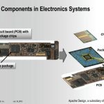
The next article is based on a success story, where “Samsung turned to Cadence to reach the speed and productivity goals they’d established for SSD validation. Cadence recommended using the Palladium XP simulation-acceleration use model together with Accelerated VIP (AVIP) for PCI Express. Samsung already used Cadence simulation VIP thus simplifying the transition to AVIP.” This story is interesting as it put the focus on three Cadence’ products: PCIe VIP (at the design stage), Palladium XP (simulation-acceleration) and PCIe Accelerated VIP (AVIP). Just to remind us that, if Synopsys has started to attack Cadence on the VIP market with a couple of acquisition during the last 12 months, Cadence is defending the position. I would guess that Samsung is a large customer, don’t you? As a side question, I would be very interested to know who has designed the PCI Express IP. It could have been designed in-house by Samsung…
Obviously, it would have been a strong move in the chess game between Cadence and Synopsys, if Cadence could have also supported the design IP for NVM Express. Denali has been one of the very first to invest in the Nand Flash controller IP development, that is now called NVM controller, as well as one of the actors in the PCIe controller IP segment. Once again, like with the DDRn IP, the PHY IP was missing to form an integrated solution, but this gap has been closed by Cadence, as they have recently announced the support of PCIe Gen-3 PHY in advanced technology nodes, see here. But, as of today, Synopsys is still the clear leader in the PCIe IP segment, even if they had to acquire the PCI Express Gen-3 PHY technology from MoSys, as blogged here some time ago… which could be an indication about how they are comfortable with PHY IP designed internally.
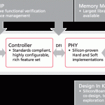
Just a word from Martin Lund, as this is the 3[SUP]rd[/SUP] article in the September newsletter: “Cadence combined our expertise in interface IP, analog/mixed signal technologies, and system verification to offer customers a complete and full-featured NVM Express interface subsystem,” said Martin Lund, senior vice president, Research and Development, SoC Realization Group, Cadence. “Without this subsystem approach, SoC designers would need to source their interface component IP separately and drive integration on their own, often increasing their design risk and overall development time for new SoCs.”
Coming back to the chess game, my personal conviction is that the “Queen” will be the PHY IP, as the company being able to provide an integrated IP solution, PHY and Controller, should be able to run the game. You may prefer to put it this way: the company unable to provide a PHY (supporting the latest standard release like PCIe Gen-3 or MIPI M-PHY) on the most advanced technology node, will most certainly lose the game, on the long term… Finally, so far, the game is slightly changing: after Synopsys incursion in VIP, Cadence has to defend their position (using “communication bullets”), on the Memory Controller IP segment, both companies are now competing head to head, when on the PCI Express IP segment, Synopsys’ dominant position begin to be challenged by Cadence, as they provide a more consistent solution, because integrating the PHY IP, than Denali, only providing the digital part. Guess what? The game is far to be over, and I am anxious to see what will be the next move, so I will look at the M&A news from both companies.
Eric Esteve from IPNEST –