When Cadence acquired Sigrity in 2012, two motives were involved: get more competitive in state of the art signal integrity analysis, and grab a foothold into the other vendor’s PCB flows in an area that is developing as a real sore spot for digital designers.
Just as the days where PCB tape-out meant actually using tape are over, so are the days where design teams can blithely make a gigantic ground plane, place parts around a board, and toss a few decoupling caps around until it feels good. Operational frequencies are routinely in the GHz range, with some interfaces at 10Gbps and rising. Margins are dropping as supply voltages get lower and lower in advanced process nodes.
The need goes even deeper now. FPGAs and SoCs, which on the one hand consolidate logic and simplify I/O routing, now need to be analyzed for possible rerouting pre-silicon to solve potential PCB layout issues. In even darker arts, IC packages are now significant contributors to signaling issues, and simplistic rules and fixes for electromagnetic interference (EMI) stop working with higher frequencies and reduced geometries involved.
There are many Sigrity tools now in the Cadence fold, and the functionality has been brought into the Cadence Allegro suite as add-ons, with tighter integration and more features on the way. One tool designers should look at very carefully is Sigrity PowerSI.
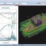
Most designers equate signal integrity analysis with high-speed SerDes designs, and are programmed to stare at eye patterns until blue in the face. Important, yes, but analyzing a SerDes is only one of many different signal integrity issues. Other issues that crop up frequently are simultaneous switching noise (SSN), coupling between geometries, power and ground bounce, and more. These are inherently dynamic issues that aren’t exposed in a DC analysis, and have to be looked at frequency domain to gain a complete understanding.
Sigrity PowerSI is not a magic wand that will cure all issues once given a set of constraints, but it is a tool that will guide designers into problematic areas of a design quickly before committing to board prototypes.
For instance, decoupling capacitors are always a fight between engineering and manufacturing, right? Too few and the design wobbles like a Weeble and isn’t stable enough to yield well in production test. Too many and people start complaining about overdesign and added material cost, even when there aren’t problems in production. Most designers set up rules like X caps per square inch, and bend those around higher current draw parts and difficult place/route packages. With Sigrity PowerSI, you know if you have too few, too many, or improperly placed decoupling caps, with quantitative results.
Designers can also model things like the processor to high speed memory interface, including connectors and packaging effects. For something like a DDR3 interface, the effects of various loading and bus frequency options can be evaluated, in frequency domain using S-parameter data extracted from the specifics of the layout.
More capability for analyzing distributed voltage and ground planes and EMI coupling between planes, traces, and vias exists in Sigrity PowerSI. IMO, the tool could potentially pay for itself in layer reduction, EMI testing, and production yield – plus helping designers visualize areas of a design that are working or problematic, removing the guess factor.
Is signal integrity as big a problem as we think in PCB design today? Have you used Sigrity PowerSI, and in what PCB flow? How does its capability compare to that of other tool sets for signal integrity analysis? What other problem areas need better analysis tools? Share your thoughts.