The 20th annual Electronic Design Process Symposium (EDPS) held April 18-19 at the Monterey Beach Hotel in Monterey California was an unqualified success. I know this because a bird (seagull?) sitting on the window sill of the conference room was so captivated by the fascinating insight provided by a number of luminaries that it joined in the conversation and could not wait to tweet about it. OK, you know I am making up stories here but the truth is that it was a great conference full of technical content, lively debate, deep dives, great perspectives, geeky humor, clever one-liners and wonderful settings. I was there and I must admit I enjoyed the event a great deal.
The event program consisted of five modules as follows:
- ESL & Platform
- Design Collaboration
- 3D–IC System Design
- FinFET: Design Challenges
- FinFET: Foundry Design Enablement Challenges
The last 2 modules occurred on the 19th, a day designated as Foundry Day: FinFET Design Enablement. The first day opening keynote was given by Ivo Bolsens, Xilinx CTO and was entitled: “The All Programmable SoC – at the Heart of Next-Generation Embedded Systems”. Gary Smith, of Gary Smith EDA delivered a dinner keynote entitled: “Silicon Platforms + Virtual Platforms = An explosion in SoC design” and Semiwiki’s Daniel Nenni had a keynote on Foundry Day entitled “The FinFET Value Proposition”. Three panels were held those 2 days as well.
The sheer number of content calls for a multi-part series of posts to follow this one describing the insight and interaction of the sessions. In this post, I will only summarize Ivo Bolsens’ presentationand its key takeaways. All the event presentations are posted here.
Ivo made the case for the new FPGA age of All-Programmable SoC. He outlined the unstoppable march down the technology curve with a pipeline of ever shrinking technology nodes from 32/28nm to 5nm where novel materials and esoteric technologies will kick in at the end of this pipeline. This lead to highlighting the ever increasing cost of implementing chip design as process nodes shrink, reaching more than $170M in 28nm. He showed an interesting Infographic slide entitled “What Happens in an Internet Minute?” depicting the staggering data growth.
An interesting factoid was that Google changes/refreshes data centers every 2 years. Facebook does that every 8 months. The Data Center is integral to business success now and is no longer viewed as a cost center.
Security is more important. People these days talk more about latency than server capacity.
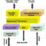
We have reached the age of All Programmable in One. Zynq’s programmable I/Os, logic, CPUs, with different granularity allowing you to tailor your application to what you need. FPGAs and CPUs have grown much closer. FPGA was a slave to the CPU, now the new FPGA is more of a peer. FPGAs can now program a function, like FPGA at CPU bus, but right on the CPU bus, not further away.
Ivo added that we are moving from dumb pipes to smart networks. The wired infrastructure is evolving to software defined networks. The Data Center infrastructure is moving to the cloud. Ivo also discussed Vivado IP integrator , and Zynq in wireless digital front-end.
Ivo’s take-aways were that the FPGA is Entering the Era of the All Programmable SoC:
- Modern FPGA is an All Programmable SoC
- Software Centric Design Flow
- Unmatched Performance/Watt
- Towards Heterogeneous Multi-Core
- Targeted Teaching Platform
I could not agree more. In fact I see us soon talking about All Programmable SoS (System of Systems), software defined, hardware realized with programmable everything: CPU, GPU, FPGA, Memory, I/Os. If the SoS term takes off, you heard it here first. If not, you heard it here last..
Fair disclosure: All transcription errors are mine, I was part of the EDPS organizing committee, and I was a presenter.
Please post your EDPS 2013 Monterey questions, comments, and trip reports HERE!
lang: en_US