
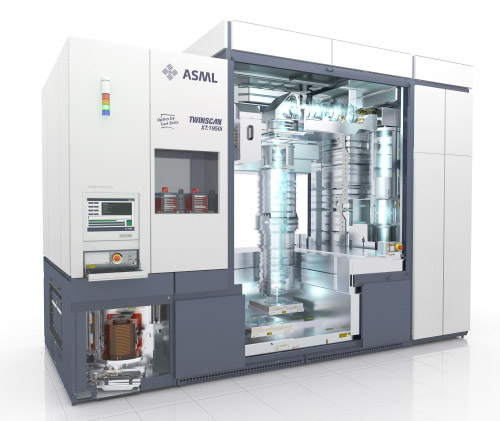
 At Semicon a few weeks ago the big news was that Intel was making a big investment in ASML as a way of funding two development programs: extreme ultra-violet (EUV) and 450mm wafers. This week TSMC announced that they would join the program too, committing 275M Euros over a five year period. They are also taking a 5% stake in ASML. ASML have said that they are also talking to some other smaller vendors.
Both these investments are a sign that the traditional model of funding semiconductor equipment is broken. Historically, the equipment companies would fund the investment out of their revenues and recover it by selling equipment. Two things have changed though. The first is that the cost of the development has grown huge, too risky for the equipment companies to undertake on their own without a level of risk sharing with the semiconductor manufacturers. The other problem is that nobody knows how many more process generations there will be that use this new generation of equipment.
In effect, the equipment industry is no longer generating enough profits to fund the investment needed for the future and it is unclear whether there are enough process generations still ahead to recover the cost of that investment.
I’ve said before that there are a lot of risks in EUV. The one that gets all the attention is that the light sources are one to two orders of magnitude dimmer than they need to be. However, two problems with masks also seem severe: mask blanks are not defect free and any particle that gets on the mask is in the focal plane of the mask and so will print, unlike refractive masks that have a pellicle to keep particles away from the plane of the mask itself.
450mm is also a big risk. SEMATECH estimates that the 300mm transition cost between $25-30B and it is not clear if that is actually being recovered. The transition to 450mm is even more challenging. Every piece of equipment must be changed, a huge number of test wafers will need to be manufactured. If EUV works as advertised then we will have a single patterning technology so that each layer on the wafer only needs to be processed once. However, if EUV does not deliver then we will continue to need to use double, triple, quadruple patterning. There are some economies of scale with 450mm since the wafers only need to be changed in the stepper half as often, but a die exposure takes the same length of time whatever the size of the wafer and so each layer of the wafer benefits little from the increased wafer size during lithography.
But the biggest challenge with 450mm is just how many more process generations there will be before we need to go to something different that uses, presumably, different equipment. The earliest that EUV and 450mm wafers might arrive is to be retrofitted to 14nm. It is already too late for the first scheduled 14nm production. At Semicon an Intel fellow said that they are basically almost freezing the design rules for 9nm with the assumption that EUV will not be available and assuming multiple patterning will be required.


TSMC CoWoS versus Intel EMIB Semiconductor Packaging