I could have written the sequence of the title in reverse order, but no, design is the one which initiates the need of a particular flow and the flow needs support of EDA tools to satisfy that need. It’s okay if the design is small; some manual procedures and workarounds/scripts may be able to perform certain jobs. However, as the design becomes complex and its size increases, it needs systematic, established, fast, accurate and automated set of steps which can complete the chip in a reasonable time and provide high yield.
This week, it was another interesting opportunity for me, listening to a DAC 2013 presentation (in the form of a webinar) of GLOBALFOUNDRIES in association with ANSYS-Apache. It’s a typical collaboration in semiconductor industry where a chip designer as a customer and an EDA tool provider as a supplier work closely as a team throughout the design cycle to produce something whose end consumer is several chains down the line.
[Simplification of blocks by abstraction – schematic diagram]
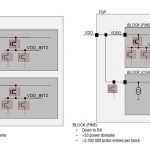
Dr. Hendrik Mau of GLOBALFOUNDRIES explained in very simplistic terms about the complexity of their power-gated, multi-domain design at 20nm node and how they have been able to abstract it into simpler blocks to determine the overall IR drop within acceptable limits of accuracy and reasonable time. It’s a 64Mbit SRAM with 128 blocks, 6528 power domains and more than 2.3M pratio entries per block. Now determining 6528 internal power nets and analyzing IR drop at transistor level for VMIN (the minimum voltage at which an array of bits can successfully be written and read at a specified yield target) characterization of the design is a huge task. Even a tool, if run on flat design will consume more than 512GByte of main memory and several days to complete. So, there come the techniques to simplify blocks by abstraction and use hierarchical approach with the assistance of automated tools to do the jobs at each step. As we see in the picture above, a block can be simplified into a coarse block that reduces the number of power domains and restricts analysis up to a higher level of metal.
[Flow established at GLOBALFOUNDRIES]
In the above flow, Calibre from Mentor has been used for extraction of hierarchical netlist, which specifies actual locations and orientations of the cells. Apache tools have been used in the successive steps. APLMMX finds out all internal power nets connected to transistors, reads extracted netlist and generates GDSII files. APLSW does switch cell characterization and generates model for the switch depicting actual resistance. Then Totem reads in GDSII file and generates LEF/DEF for the blocks and the top level. Now Totem reads the LEF/DEF and the switch cell model to generate the IR drop.
[Hybrid Approach – GDSII view and view in Totem; IR drop results of 64Mbit SRAM]
GLOBALFOUNDRIES used a hybrid approach having 4 fine blocks in the middle surrounded by 124 coarse blocks. IR drop in metal M6 with all blocks consuming same power and whole design connected through wire bond is elliptical, where as it is increased in M1 and M2 in the fine blocks at the center.
[Comparison of run time and memory requirements in flat and hybrid approach]
The hierarchical hybrid analysis of a smaller design of size 8Mbit (which could be run in flat mode) with 4 fine blocks and 12 coarse blocks shows that compared to flat run it consumes lesser than 7.5x peak memory and takes lesser than 4x run time, while maximum IR drop remains close to that of the flat run.
It’s a classic example of how automatic switch tracing can simplify handling large designs and the use of hierarchical hybrid approach can reduce memory requirements and execution time for IR drop analysis. GLOBALFOUNDRIES has been able to successfully use this flow in 28nm and 20nm designs and is now using it in 14nm designs. Details about the design, flow, and tools can be found in the presentation titled “Hierarchical Voltage Drop Analysis Techniques for Complex Power-Gated Multi-Domain 20nm Designs” here.