llmda newsletter ad (2)

Full Chip ESD Sign-off – Necessary

Full Chip ESD Sign-off – Necessary
by Pawan Fangaria on 11-13-2013 at 7:00 pm

As Moore’s law keeps going, semiconductor design density on a chip keeps increasing. The real concern today is that the shrinkage in technology node has rendered the small wire geometry and gate oxide thickness (although fine in all other perspectives) extremely vulnerable to ESD (Electrostatic Discharge) effects. More than 1/3[SUP]rd[/SUP] of chip failures happen due to ESD. An IC can be exposed to ESD either from transfer of charge from external sources such as human interaction (tested by HBM, i.e. Human Body Model) and machine handling (tested by MM, i.e. Machine Model) or from internal built up of charge leaving through the package (tested by CDM, i.e. Charged Device Model). While I/O interface is most vulnerable to ESD, entire internal circuit of IC in under risk. Major damages such as gate oxide breakdown can lead to immediate failure whereas wires and vias can wear out over time.

It’s important and essential to protect the circuitry inside an IC from dielectric breakdown. Typically clamp circuits are placed at the I/O and P/G pads which can handle large transient current, provide efficient discharge path to ESD current and prevent any pin voltage from exceeding the oxide breakdown voltage.

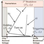
In the I-V characteristic of a typical ESD protection circuit, the dotted line curve represents the response of a turn-on device and the solid line curve represents the snap-back characteristic of a NMOS ESD device. It’s important to note that with technology migration the oxide breakdown voltage continues to move towards left while the thermal failure limit continues to move down, thus imposing severe constraint on the protection (clamp) circuit to operate in that compressed region.

With increasing design size and complexity at lower nodes, design of ESD protection circuit is becoming increasingly complex requiring planning and verification at full chip level for all P/G nets along with ESD clamp cells and the package. The pin-to-pin paths that do not meet the defined limits should be highlighted and connectivity or routing issues must be identified with accurate resistance or impedance calculations. Current density in wires from any ESD event must be accurately estimated to ensure that the wires will not fail from such high levels of current flow.

Apache’sPathFinder provides a robust comprehensive planning and verification for ESD at full chip level which ensures that connectivity between any two pins meets design guidelines. It performs connectivity analysis for HBM, MM and CDM discharge events and predicts the current density in all wires and vias. By leveraging Apache’s RedHawk (for digital designs) and Totem (for analog designs) tools, PathFinder provides unprecedented capacity and performance for simulating large SoCs and custom designs.

During HBM or MM check, PathFinder estimates the effective resistance between any two pins in the circuit by traversing the network through one or more clamp cells placed between these pins. This is done very accurately by taking into account the clamps which pass the loop resistance threshold between two pins and can effectively provide discharge pathway; parallel R is considered between the two pins.

In case of CDM check, PathFinder calculates the resistance of the path between any device to VSS or VDD to device and also loop resistance between device VDD pin to clamp cell VDD pin, clamp cell VSS pin to device VSS pin and the resistance of clamp cell itself.


Current Density Checks are very important to save wires and vias from electro migration. PathFinder identifies clamp cells between pin pairs that are effective in conducting current and then calculates the current through the wires and vias connected to these pins or pads by injecting the current into the pads as per ESD standard definition. In then highlights the wires and vias that fail the current density limits prescribed by the technology process.


[Textual and Graphical reporting of issues – VDD route from a logic cell to a clamp cell fails defined resistance limit]

PathFinder reports the analysis results in text as well as graphical form. It highlights weak areas and resistance bottlenecks in the design and helps designers in fixing those without leaving PathFinder environment. An interactive ‘what-if’ analysis can be carried out before committing to layout. There is a whitepaperon Apache website which provides great level of details about ESD and the solution for full-chip ESD integrity analysis, verification and fixes. After reading this paper, I could gain more insight into ESD phenomenon which I did not have earlier. Interesting read!!

More Articles by Pawan Fangaria…..

lang: en_US


Bringing EDA to India

Bringing EDA to India
by Daniel Payne on 11-13-2013 at 1:00 pm

Why do all three big EDA companies have user group meetings in India? The answer is to grow the EDA market in India because so many multi-national companies have engineers in India doing SoC, and IP design work. In my 35 years of IC design and EDA experience I’ve had the pleasure of working with and knowing many engineers and managers from India.

According to an EDAC report the software industry in India has been growing from humble beginnings over the past two decades:

  • Call centers
  • Data management
  • Accounting software
  • Market analysis and consulting
  • Medical diagnostics
  • Semiconductor design
  • EDA
  • CAD in auto and aerospace application

The other recent trend is India-based companies doing their own semiconductor IP design for export: Open-Silicon, Ittiam, Cosmic Circuits.


Source: EDAC Report

Here are the big three EDA user group meetings:

User2User India
Next month in Bangalore, India you can attend the Mentor meeting and learn from all of the technical sessions, watch product demonstrations, then network with other IC design professionals.

The two big-name speakers are Walden Rhines, CEO of Mentor Graphics, along with Taher Madraswala, SR VP of Engineering at Open-Silicon.


Walden Rhines, Mentor Graphics


​Taher Madraswala, Open-Silicon

There are 24 presentations divided across four tracks:

  • System Design (Aricent, HCL, Honeywell, L&T Infotech, Harman)
  • Functional Verification (Cypress Semi, Microsemi, Vitesse Semi, Ericsson, Xilinx)
  • Physical Verification (Xilinx, AMD, IBM, STMicroelectronics, ARM, Broadcom)
  • IC Implementation and Test (AMD, STMicroelectronics, Cypress Semi, ARM)

The full agenda is here, along with registration.

Keynote
Mr. Rhines will speak about The Big Squeeze, how to keep the progress of Moore’s Law by showing a mathematical basis for the challenge, using a dry sense of humor, and showing a roadmap of what the future may bring for the next decade in semiconductor design.

Conference Advisory Board
Organizing such a large conference requires many volunteers, and the 24 technical presentations were selected by nine members of a Conference Advisory Board, represented by the following companies: Marvell, Xilinx, Qualcomm, Intel, STMicroelectronics, Open Silicon, Freescale, Wipro Technologies and Honeywell.

More Articles by Daniel Payne …..

lang: en_US


ASICs for Bitcoin Mining!

ASICs for Bitcoin Mining!
by Daniel Nenni on 11-12-2013 at 8:00 pm

One of the hottest areas for Application Specific Integrated Circuits today is Bitcoin mining. A good friend of mine has a son who is involved in a Bitcoin start-up so we have been discussing this at great length and I will share what I have learned thus far. Coincidently, my wife asked me about Bitcoin during our most recent walk down the Iron Horse Trail. Since I had recently researched it (unbeknownst to her) she now thinks I’m the smartest guy in the world, so I have that going for me.

Bitcoinuses peer-to-peer technology to operate with no central authority or banks; managing transactions and the issuing of bitcoins is carried out collectively by the network. Bitcoin is open-source; its design is public, nobody owns or controls Bitcoin and everyone can take part. Through many of its unique properties, Bitcoin allows exciting uses that could not be covered by any previous payment system.

If you don’t want to buy Bitcoins for $300-400 apiece you can mine them by solving increasingly complex problems. Bitcoin miners are paid in transaction fees as well as newly minted coins. Mining is a very compute intensive process by design so the number of new Bitcoins generated is manageable, secure, and somewhat tamper-resistant. The first mining wave used whatever CPU was on a desk or lap. GPU mining was next as it is significantly faster and required much less power to operate. In parallel FPGA mining emerged as an even lower power option to GPUs and were much more optimizable. Now ASICs are being used to mine Bitcoins which are proving to be vastly superior to CPU, GPU, and FPGAs.

ASICs have been around since the 1980s and have been a pivotal technology in the growth of the semiconductor industry. In fact, there is a dedicated ASIC chapter in our book “Fabless: The Transformation of the Semiconductor Industry”. The current success based ASIC business model, which was perfected by eSilicon, allows a minimum upfront investment with a royalty attached for packaged chips, which fits perfectly for emerging technologies such as Bitcoin mining. Current Bitcoin ASICS use 28nm LP to better manage power. The next generation FinFET based ASICs which are inherently lower power will be ideal for mining, absolutely.

If you want to get started in the Bitcoin world, just for research purposes and not for criminal activities of course, here is the best place: TRYBTC. Full disclosure: As you dig into the site you may notice that one of the creators was also an early developer for the Semiconductor Wikipedia Project.

I’m not personally convinced that Bitcoins will survive the onslaught of criminal attempts to control or use them. In fact, due to the huge criminal element that surrounds Bitcoin today, they could be made outright illegal. I am convinced however that there is money to be made selling Bitcoin related silicon. As with the California gold rush in the 1850’s, the miners didn’t necessarily get as rich as the people who supplied them right?

More Articles by Daniel Nenni…..

lang: en_US


A New IC Power Integrity Tool

A New IC Power Integrity Tool
by Daniel Payne on 11-12-2013 at 7:00 am

In EDA we have come to expect that only small start-up companies create new tools, however a team at Cadencehas developed a new IC power integrity tool called Voltus from scratch. To learn more I spoke last week with KT Moore, a Group Director at Cadence. I’ve known KT for over a decade, and first met him when he was at Magma marketing their FineSIM circuit simulator.


KT Moore, Cadence

Continue reading “A New IC Power Integrity Tool”


Is FD-SOI Really Faster, Cooler, Simpler?

Is FD-SOI Really Faster, Cooler, Simpler?
by Eric Esteve on 11-12-2013 at 5:17 am

I love the slogan associated with FD-SOI: the technology is supposed to be Faster, Cooler, Simpler. Does this slogan reflect the reality? Let’s start with Simpler. We (the semiconductor industry) have the perception that Silicon On Insulator (SOI) technology is something complex and exotic. Why? Because SOI has been used to design some expensive photonic or power devices, and also by AMD since 2003 to process the 64bit Processor, rather complex design. This is a perception, let’s see what is the reality.

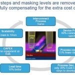
In the real world, FDSOI technology requires using more expensive SOI wafers. Then, moving from 28nm bulk to 28nm FD-SOI, means that 90% of the process steps will be identical, and the same manufacturing tools can be reused. The story becomes to be interesting when you realize that several process steps and masking levels are removed from 28nm bulk… So, saying that 28nm FD-SOI is Simpler than 28nm bulk is true.

Is FD-SOI Cooler than bulk? Cooler meaning less leakage induced power consumption, and less operating power. In fact, FD-SOI enables very low voltage operation, but the device is extremely fast at low voltage, running with better energy efficiency. For example, the same design running at 0.82V on FD-SOI will reach the same performance than under 1.0V on bulk, exhibiting 35% less dynamic power and 35% less leakage power in stand-by.

Gate Leakage is lower for FD-SOI, and we can identify the rational if we look at the above picture:

  • Gate dielectric is thicker, with a direct impact on the gate leakage current
  • Leakage current is less temperature sensitive with FD-SOI

That’s why it’s possible to design ultra low power SRAM memories on FD-SOI technologies, for example.

Finally, FD-SOI has lower channel leakage current, once again the above picture help understanding that the carriers are efficiently confined from source to drain: the buried oxide prevent these carriers to spread into bulk.
It look like FD-SOI is really cooler than bulk. Let’s check now if FD-SOI technology is also Faster.


Semiwiki readers have already seen the above picture in a previous blog, this version is just more synthetic. ARM processor has seen a 35% performance increase at nominal and high voltage, the performance going up to 2X at low voltage.

Nothing magic to explain such a faster performance, only physics laws: the source to drain channel being shorter, electrons can go faster from source to drain!

Finally, FD-SOI enables usage of body bias techniques, as illustrated on the above picture. Thus, the transistor can be ideally controlled through two independent gates. These body bias techniques allow dynamically modulating the transistor threshold voltage.
Does FD-SOI technology allow designing faster devices? These examples show that the answer is clearly yes!

Faster, Simpler, Cooler, but what about the cost? I plan to shortly propose a step by step explanation explaining why such a faster, simpler and cooler FD-SOI technology is also more cost effective than bulk.

From Eric Esteve from IPNEST

More Articles by Eric Esteve …..

lang: en_US


Xilinx Begins Shipping TSMC 20nm FPGAs!

Xilinx Begins Shipping TSMC 20nm FPGAs!
by Daniel Nenni on 11-11-2013 at 10:00 am

Xilinx just announced the shipment of the first TSMC based 20 nm FPGAs, beating Altera to the punch yet again. Xilinx was also the first to ship TSMC 28nm FPGAs and will undoubtedly beat Altera to 14nm which could be the knockout punch we have all been waiting for. The Xilinx UltraScale is a new family of FPGAs that will use 20nm and 16nm processes with 20nm samples available just in time for Christmas! Ho ho ho…

“This announcement underscores our first-to-market leadership commitment of delivering high-performance FPGAs,” said Victor Peng, senior vice president and general manager of products at Xilinx. “The next generation starts now with the shipment of our new UltraScale devices, building upon the tremendous momentum we have established with our 7 series.”

“The delivery of UltraScale devices on TSMC’s 20nm process technology marks a new juncture for the semiconductor industry,” said TSMC vice president of R&D, Dr. Y.J. Mii. “We are happy to see Xilinx continue to break new ground and deliver 20nm silicon to its customers.”

In 2012 the FPGA market was about a $4.5 billion business. Xilinx has about 50% market share at $2.2 billion. Altera is not far behind at $1.8 billion. Being the first to silicon is key in the FPGA world as it not only builds market share, it also builds trust that Xilinx can continue to deliver leading edge products.

Xilinx and longtime manufacturing partner UMC were about one year late at 40nm which allowed Altera and manufacturing partner TSMC to gain significant FPGA market share. Xilinx then switched to TSMC at 28nm and the race with Altera on a level manufacturing playing field began. Clearly Xilinx won 28nm with not only first silicon shipped but also first to 3D IC technology.

One of the big questions I see around the internet is: “Why did Altera really switch to Intel for 14nm?” Simple: Because Altera cannot beat Xilinx to market on a level manufacturing playing field. Even though Altera is a long time TSMC partner, TSMC does not play favorites and delivered technology to both Altera and Xilinx in a uniform manner.

As previously reported, Intel 14nm is late. Word from Altera is that they won’t start taping out 14nm designs until Q4 2014. Xilinx, on the other hand, is taping out 16nm designs early in Q1 2014. Intel is not talking in detail about the speed and density of 14nm in regards to their foundry business so I have no idea how competitive Altera will be against Xilinx at 14nm. But Altera being a year or more late to market is 40nm all over again.

More Articles by Daniel Nenni…..

lang: en_US


Semiconductor Fabrication Module Optimization

Semiconductor Fabrication Module Optimization
by Pawan Fangaria on 11-11-2013 at 9:00 am

The growing process integration complexity at each technology node has increased development time and cost, and this trend looks to continue. There is a looming risk of delivering unrepeatable critical unit processes (or process modules) that would require revisiting development and manufacturing requalification or in severe cases a design re-spin. Below the 22nm process node, tremendous effort is necessary to meet process integration specifications with a yielding process that is robust in the face of unavoidable manufacturing variation.

In one of my earlier articles here, I talked about a quick and automated way to optimize the complex BEOL (Back-End-Of-Line) metallization process through the use of Virtual Fabrication provided by a state-of-the-art tool, SEMulator3D from Coventor. A BEOL metallization whitepaperillustrates the SEMulator3D platform capability to assist with process development and optimization. SEMulator3D is an extremely powerful Virtual Fabrication tool to perform all types of tasks related to complete semiconductor chip manufacturing process, including FEOL (Front-End-Of-Line), MOL (Middle-Of-Line) and BEOL processes, quickly at your desk.

As Virtual Fabrication becomes increasingly important to help development keep pace with Moore’s Law, the semiconductor design and fabrication community are eager to understand more about how to leverage this technology. In the most straightforward sense, this means replacing costly and lengthy iterations of build-and-test learning with rapid virtual experimentation on a laptop. The ability to comprehensively map out an entire module space across all the critical structures on the device (in a matter of hours or days) is a significant innovation to help be the first to market with a new technology. Last month, Ryan J Patz from Coventor, author of BEOL metallization and patterning whitepapers, gave a very informative and detailed presentation on how Virtual Fabrication is done for BEOL module optimization below the 22nm technology node. The presentation was done live at AVS 60[SUP]th[/SUP] International Symposium & Exhibition. I was delighted to go through the presentation slides at the Coventor website here.

The talk provides a procedure for setting up a Virtual Fabrication process flow with automation for process module optimization. Mr. Patz presented example cases of how to use the SEMulator3D platform for identifying unexpected yield detractors, tuning cross-wafer uniformity, optimizing a process module for maximum yield and closed with a proposal to use Virtual Fabrication for feed-forward control to drive down run-to-run variation. Below, I am reproducing some of the key aspects of fabrication discussed in the presentation.


[Virtual Fabrication Automation Setup]

The above picture shows the automation capability to run a large number of experiments varying multiple parameters using a single spreadsheet-based input. Virtual Metrology collects all desired measurements from each model. It was noted that metrology not only includes the standard in-fab measurements (e.g. CD, film thickness) but also measurements that require destructive analysis on silicon, such as cross-section or interface area.


[Unit Process Tuning – Via Chamfer]

The above picture shows the results of a via chamfer study. The findings matched existing unit process trends, and Mr. Patz went on to discuss additional testing that could be done using Virtual Fabrication that is not easily done on silicon. For example, chamfer sensitivity to changes in CD or the Low-k porosity could be explored with simple changes to the inputs. This data cannot be generated on-wafer until the next technology generation. Results of these simulations give a better understanding of the process window and indication of future challenges.


[Process Interaction – TiN hard Mask Impact on Metallization]

The image above shows the trend of liner thickness for varying M2 TiN etch ratios. The large number of experiments gave insight into an unexpected process integration trend. The Cu cross-section area decreased with increased TiN etch rate, a change that was expected to improve Cu fill. Inspection of the 3D model revealed the effect was driven by a “shoulder” in the dielectric cap layer, resulting in a metallization profile degrade. This type of characterization helps to predict, and more quickly solve, yield issues that arise during a manufacturing ramp.

Digging further into process integration, the picture below shows how V1-M1 contact area varies with lithography. This model showed that a variation in the range of -3nm to +3nm in M1 lithography bias resulted in a 3x variation in contact area. The remainder of the presentation focused on understanding the drivers of V1-M1 contact area in order to minimize variation.


[V1-M1 contact area]


[Cross-Wafer Uniformity – V1-M1 Contact Area Baseline]

The general point was made that Virtual Fabrication is necessary to predict how all upstream process variation will impact a downstream process, such as V1-M1 contact area. This example showed upstream unit process variation resulted in a 5.9% 1s variation in the V1-M1 contact area. The key unit processes to control the contact area were identified, and an 1125-run experiment helped determine the steps in those unit processes most important for V1-M1 contact area.


[Cross-Wafer Tuning – Module Level Optimization]

Mr. Patz proposed retargeting the key unit process steps away from minimized non-uniformity to reduce the contact area variation. It was surprising to see that moving one of the steps in the V1-M2 etch from 0.0% to 20.7% 1s non-uniformity actually cut the V1-M1 contact area variation in half. This result was helpful to explain why understanding interactions within an entire module could be a key enabler for feed-forward process control.

Virtual Fabrication can help semiconductor design and process engineers characterize process variation sensitivity at the design stage, tune cross-wafer uniformity and optimize processes at a module level in much less time. This detailed characterization may even help bring in the era of automated process control (APC) and feed-forward process control to reduce device variation and improve yield. Have a look at the detailed presentation here. Also of interest would be another whitepaper on BEOL patterning. Happy learning!!

More Articles by Pawan Fangaria…..

lang: en_US


The Pelican Has Landed: Formal on an Unannounced ARM Processor

The Pelican Has Landed: Formal on an Unannounced ARM Processor
by Paul McLellan on 11-10-2013 at 3:00 pm

At the Jasper Users’ Group, Alex Netterville of ARM presented about how ARM are using formal on an unannounced processor code-named Pelican. Don’t read the presentation trying to find out information about Pelican itself, there isn’t any. That wasn’t the topic. Alex has been using formal approaches for 10 years and worked on the ARM Cortices R4, A9, A5, and M0+.


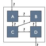
The approach he discussed was using formal approaches for all interfaces, precisely stating the way that the interface between two subsystems should behave, and without peeking inside the subsystems. These definitions have to exist or nobody can design the subsystems, but word of mouth is a terrible way to do it, a Word document is better since at least it is written down and changes can be tracked, but a writing formal properties is the best since it is executable and it is possible to check whether the subsystems do indeed implement the specified behavior (subject to some caveats, of course).


At the start of the project the interface specs are owned by the microarchitects. Unit level designers share ownership throughout the project, keeping them up to date along with the RTL. But before RTL is written, they allow a formal bench to be created and block I/O behavior to be examined with Jasper Visualize.


Properties need to be written in a way that adapts to the environment. If only one block is present they are checking either the outputs or the inputs (depending on which block it is) and assuming that the other block (which isn’t present) is correct. If both blocks are present they are eavesdropping on the traffic and checking it conforms.


Specifications are simple and non-verbose, using a pseudo language that was created with an optimal set of keywords. From that they can generate OVL, SVA, Jasper TCL etc. The typical size of one of these “.i” files is from tens of lines to thousands of lines. But the generated files are typically 4-6X bigger.

The interface specifications are used at several levels. At the unit-level, when a block is isolated from its environment, it is used to constrain inputs and check outputs. At the top level (or higher levels) it is used to check the interaction of sub-blocks.

One challenge with formal at ARM (see my earlier blog) is lowering the barriers to adoption so that designers use it. The test environment makes it easy to specify the test hierarchy, methodology and the configuration. Underlying Jasper-specific TCL then automatically builds and configures the appropriate design.

When all the blocks are put together there are often problems where tests either pass at the unit level but fail at the top level or vice versa. If it fails at the top but passes at sub-level then the assumptions at the input of a block might be too strong. The other way around, where they pass at the top but fail at the sub-level is because the assumptions at the input of the sub-block are too weak.

So what are the issues with this interface-centric methodology.

  • Isolated unit level formal benches may not model the environmental context of that unit in the final product correctly in projects that don’t adopt this methodology
  • Clocks and resets may not be attached to the correct interface specification
  • System level modelling at top can sometimes be a compromise that doesn’t catch all use cases.
  • A signal might be missing from an interface specification

There is more in the presentation. If you are a Jasper user (not necessarily one who attended JUG) then you can download the presentations, including this one, here.


More articles by Paul McLellan…


IP-SoC 2013 Top Class Presentations…

IP-SoC 2013 Top Class Presentations…
by Eric Esteve on 11-10-2013 at 10:41 am

… were given to an ever shrinking audience. This is IP-SoC paradox: audience has enjoyed very good presentations made by TSMC (for the first time at IP-SoC, as far as I remember), SMIC, D&R, Gartner or ST-Microelectronic, to name just a few. The event is well organized, on the morning you can listen to keynotes in the largest room, and select the track to attend on the afternoon between “IP Business and Trends” and “IP Design” and later between “Best IP Practices” or “From IP to SoC Architecture”. Is it because Grenoble is too far away from Airport hubs?

Let’s come back to the keynotes, with a presentation from Ganesh Ramamoorthy, from Gartner, “The Competitive Landscape of the Semiconductor IP Market, 2013 and Beyond”. I have been skeptical in the past about the market insights from Gartner, but I have to admit that this year, Gartner proposes a vision of the Semiconductor industry future which looks quite interesting. Gartner only see a few high growth segments for the Design IP market, the higher growth being associated to the Processor IP, then wired Interface and Fixed functions.

Another interesting finding is the 2012-2017 evolution of the Electronic Equipment (see picture below). If you trust Gartner, the future is not exactly promising, with only Smartphones, Media Tablet and Solid State Drive seeing a 2012-2017 unit CAGR higher than 20%…

In fact, Gartner has said that the higher growth segments are expected to be those with a low SC content, like wearable devices or Internet of Things, thus gives recommendations to IP vendors:

Before giving my own opinion, I wish to say that this analysis by Gartner represent a real work, probably resulting from intensive brainstorming. Forecasting IoT and wearable devices are the only strong growth area, and recommending to IP vendors to prepare their positioning and marketing messages to address these markets is probably true for ARM Ltd., but I have a strong doubt about the validity of this message when addressing plenty of other IP market segments, like IP Fabric or Network on Chip, Very High Speed SerDes and Interface PHY, to name a few functions expected to grow strongly. ARM Ltd. is the largest IP vendor (and will continue to grow and stay the leader)… but IP is not restricted to microprocessor core only! There are numerous IP vendors, including leaders like Synopsys or Cadence, expected to grow their business by addressing Networking, Data Computing, Telecom and also Mobile. These vendors may also address IoT or wearable devices, but I strongly doubt that these segments only will generate the strong growth they are expecting.

TSMC and SMIC have both given keynotes this year, and both presentation where very interesting, but for different reasons. TSMC presentation, clearly IP centric, very professional, delivered the key message: IP Ecosystem is the cornerstone for supporting SoC and ASIC/ASSP design. Open Innovation Platform (OIP) is the program developed by TSMC, referenced by customers for more than 10 years, and TSMC continues to extend this program. I would need a full blog to completely describe OIP and TSMC 9000, you can take a look at this previous blog: IP Quality: Foundation of a successful Ecosystem to learn more about Open Innovation Platform.

The presentation from SMIC was also interesting, for a different reason. Tian Shen Tang, Sr VP, SMIC, has delivered a sale pitch for SMIC, as expected, and this pitch was even more a China sales pitch. It was certainly a good idea to remind the audience that China is moving fast, very fast. If ten years ago western companies were searching for a low labor cost resource, Chinese OEM, semiconductor and Design IP companies are now competing with their western counterpart. It was a surprising presentation, but the message delivered by SMIC makes sense, and the company is positioning as a partner, helping Design IP to penetrate Chinese market. If you prefer, it was more a business oriented (political?) than a pure technical message, but the message was clear: China is part of the High Tech market, and SMIC can help you addressing this market.

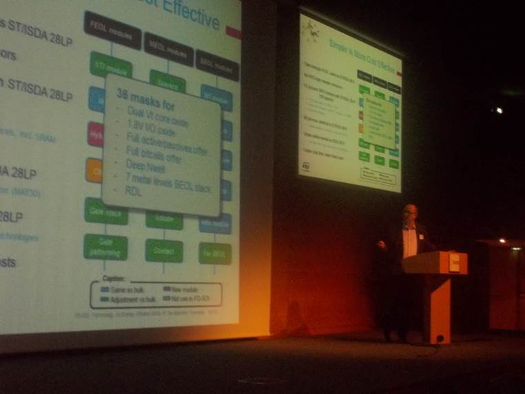
Finally, I will talk about the presentation made by Giorgio Cesana, Technical Marketing Dr with STM, about FDSOI, that we can summarize by these words: FDSOI is Simpler, Cooler and Faster. When we think about SOI, we remind the technology used by AMD ten years ago or the exotic ASIC products developed for military application. According with ST, FDSOI is, in 2013, completely different, as it’s now Simpler (planar devices to be compared with 3D FinFET), with an immediate impact in term of mask count, generating itself a direct impact on technology cost. The SOI wafers are more expensive? True! But you need less process steps and less masks (even when comparing with Bulk 28nm), so the cost evaluation per wafer is within 1% between 28FDSOI and Bulk28LP… When comparing 14FinFET and 14FDSOI wafer cost, FDSOI appears to be 35% cheaper!

If you remember this blog, you already know why FDSOI is “Cooler”, or “Faster”, thanks to Silicon On Insulator technology, the power consumption is minimized compared with Bulk. Because you can run a microprocessor faster by 20% or more, using the same power budget: FDSOI is Faster. In fact, this is just the first slides summary, so I will have to come back to FDSOI in one next blog. I had the opportunity to discuss with Giorgio, so I will have the possibility of writing well documented blog about FDSOI, stay tuned!

From Eric Esteve from IPNEST

More Articles by Eric Esteve …..


Can Intel Catch Samsung? Can Anybody Catch Samsung?

Can Intel Catch Samsung? Can Anybody Catch Samsung?
by Daniel Nenni on 11-08-2013 at 5:00 pm

As a professional conference attendee I see a lot of keynotes, some good and some bad. I saw a great one from Kurt Shuler at the SEMICO IP Impact Conference last week. Why this conference was not standing room only I do not know. Kurt’s characterization of the semiconductor industry was well worth the price of admission. I didn’t actually pay to attend of course since I’m an internationally recognized industry expert and soon to be bestselling co-author of “Fabless: The Transition of the Semiconductor Industry”. But I am certainly glad I left my Lazyboy Command Center and made the drive to Silicon Valley, absolutely.

First let’s look at Kurt. We are friends so I’m a bit biased but his credentials are very impressive. He started with a BS in Aeronautical engineering from the Air Force Academy followed by 6 years as a Navigator and Electronic Warfare Officer, Special Operations Forces. During that time Kurt was decorated for courage under fire and outstanding combat leadership after successful missions in Bosnia-Herzegovina, Iraq, and Haiti. He followed that with an MBA from MIT plus stints with Intel, TI and related technology start-ups. Recently, his current employer (Arteris) was purchased by Qualcomm for an obscene amount of money. So yes, Kurt is definitely someone you want to listen too.

Kurt’s keynote (slides) followed his recent article in EETimes “Wake Up, Semi Industry: System OEMs Might Not Need You” which highlights the changes in the semiconductor business climate. It’s a great article and the comments are worth a read too.

“Times have changed dramatically since semiconductor companies ruled the roost. Chip vendors used to control 99 percent of the chip design talent in the industry, but those days are past. In today’s world, perhaps 75 percent of the top silicon design engineers work for chip vendors and the remaining 25 percent are being snapped up by OEMs. That’s because the SoC design determines competitive advantage now more than ever, and software differentiation is not enough.”

Samsung is a frightening example as they can control the entire BOM for a variety of consumer electronics products including mobile devices and the Internet of Things. Yesterday was Samsung’s analyst day, the first one in eight years, and you can find the audio and presentation materials HERE.

“We will expand our mergers-and-acquisitions strategy beyond a few target areas to pursue opportunities across a wide range of fields,” Lee said. The company wants to “enhance the competitive edge of our current businesses and capture new chances for future growth,” he said.


In regards to the System LSI presentation (HERE), even if only half of it is true (which is about right) I do not see how Intel expects to compete with the likes of Samsung without making some revolutionary acquisitions in the very near future. Microsoft bought Nokia, Google bought Motorola Mobile, and through some key acquisitions Apple is now a leading edge fabless semiconductor company. Intel’s own investor meeting is in two weeks and they have some serious questions to answer now.

More Articles by Daniel Nenni…..

lang: en_US