In many designs, an on chip inductor is created as though it were simply a device with an L and a Q value. Of course this view would seem to make life simpler for designers and the tools they use. But in reality even a simple inductor is really a complex compound structure with many electromagnetic elements interacting in complex ways. The behavior of the actual inductor will depend heavily on the aggregate of all the effects occurring within the device.
The resulting quality of a device in a given circuit is controlled by the detailed behavior of the device. It follows that this creates a dependency on the tools used to model and design the device. It also means that the designer will need to be aware of and address the tradeoffs that are presented within the flow.
Many of the effects we see when we look closely at an inductor are frequency dependent. The very first thing we should examine is how current flow within a device is dictated by self and mutual inductance at higher frequencies. These resulting phenomena are often simply lumped together as skin effects; but they have significant impact on device behavior because of changes in effective resistance and capacitance.
We can see these effects in the current flow within the wires of a differential inductor as a function of the frequency. The difference between extraction based tools and electromagnetic solvers is that solvers are going to directly solve Maxwell’s equations for the arbitrary geometries. This will allow the calculation of currents and voltages through conductors by accounting for electric and magnetic fields passing through dielectrics, which in turn can induce currents in adjacent conductors. Extraction tools will use analytical closed-form equations to estimate the equivalent model for the structure, typically at a fixed frequency.
The lynchpin of the solver methodology is meshing. The conductors are divided into 3D shapes or cells and all current fluxes though the walls of these shapes are calculated. Inhomogeneous behavior inside the conductors becomes evident when we look at current density visualizations available in PeakView.
Any other approach will miss fine grain behavior like that shown below. Other approaches that are not solver based might also divide the structure up for analysis, but they will not properly model internal behavior and furthermore their output will most likely consist of an exhaustive enumeration of hundreds or thousands of small elements or slices. Conversely solvers output their results efficiently on a port-by-port basis using s-parameters. RLCk (“physical”) models for the system can then be fitted in an efficient and compact manner. The efficiency of these physics based models is extremely high when a physical equivalent circuit, or pi model, is used.
A partial list of parameters that affect inductor behavior and performance are topology, wire sheet resistance, wire width and thickness, wire spacing, use of vias, cross-over layer design, shields, guard rings and metal fill, to name a few. Each of these parameters interacts with the others in complex ways. This becomes an n-dimensional problem, where not only L and Q are set, but also self resonance frequency, the peak Q frequency, the slope and roll off of Q, etc.
These characteristics are weighted differently depending upon the application. Are the devices peaking inductors, part of an LC tank, high current devices, impedance matching transformers, t-coils, baluns, or even transmission lines, etc?
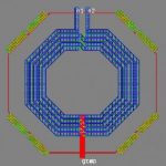
Visualizations are often the best way to understand the internal dynamics in electromagnetic devices. The images below, taken from the PeakView GUI, illustrate this quite clearly. We are using a 5 turn differential inductor with both the center tap and second port grounded. The device is shown with stimulus on the first port.
At DC we see uniform current across the active leg. The current mostly flows to the grounded center tap, but some residual current flows to the far pin which is seen on the adjacent winding.
DC Current Density
At 100MHz, there is still uniform current in the active wire, but the induced current from inductive coupling on the other leg completely counteracts the residual current.
100 MHz Current Density
At 500 MHz substantial current is induced in the grounded leg by inductive coupling.
500 MHz Current Density
At 1 GHz we see the results of skin effect as self inductance along the wire asserts itself.
1 GHz Current Density
Then finally at 8GHz we see how almost all the current is flowing in the outer edges of the wires. But more interestingly we can see that where there is an adjacent wire more current flows than on the outermost edge of the outer winding of the device.
8 GHz Current Density
This clearly shows asymmetrical currents across the wires. Upon closer examination it is possible to see reverse induced currents in the center of the wires. These eddy currents can only be properly calculated by the use of an electromagnetic solver such as PeakView.
Our analysis of this device shows that each wire starts to behave like two wires rather than one as the frequency is increased. This is a result of the current separation due to skin effect. This has an enormous effect on the Q and the L for the device.
This quick example clearly demonstrates how only an electromagnetic solver with sufficient visualization tools is up to the job of designing inductors for today’s challenging RF and high speed analog designs.
This is a whitepaper from Lorentz Solutions. You can see it and others HERE. Tom Simon from Lorentz Solutions and I go way back to the Calma days. He is my goto guy for EM, absolutely.
lang: en_US