You are currently viewing SemiWiki as a guest which gives you limited access to the site. To view blog comments and experience other SemiWiki features you must be a registered member. Registration is fast, simple, and absolutely free so please, join our community today!
The occurrences of notorious stochastic defects in EUV lithography have resulted in CD or corresponding dose windows with the lower and higher bounds being characterized as “cliffs” [1-3], since the defect density increases exponentially when approaching these bounds. The defects at lower doses have been attributed to the shot noise from absorbed photon density being too low, while the defects at higher doses can be attributed to non-EUV exposures of the resist, such as electrons, ions, and radiation from the EUV-induced plasma, or secondary electrons from the substrate [4]. In particular, the exposure to the hydrogen is known to result in etching of the resist [5,6].
Recent data [7] have shown that an increased EUV dose led to a reduction in resist thickness (after development). The hydrogen-induced etching of the resist is a low-hanging fruit for causing this effect. A higher EUV exposure dose requires slowing the wafer stage scan speed (thus also reducing wafer throughput), resulting in a longer exposure to the EUV-induced hydrogen plasma. This leads to extra etching of the resist, leading to added resist loss. The reduction in the remaining resist thickness (after develop) can be linearly fitted to the dose [8]. Consequently, the absorbed dose in this remaining thickness can be calculated as a function of the incident dose, as well as the initial thickness.
Absorbed dose
= (Incident dose)(Transmission)(Absorption)
where Transmission = exp(-absorption coeff. x [resist thickness lost])
and Absorption = (1-exp(-absorption coeff. x [remaining thickness]).
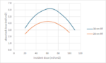
The physical understanding is clear: increased resist loss reduces the dose that is transmitted to the remaining thickness of the resist layer, and at the same time reduces the amount of resist absorption in this remaining layer. This calculation is applied to the data from [7], with initial thicknesses of 20 nm and 30 nm (Figure 1).
Figure 1. Absorbed EUV dose in remaining resist thickness as a function of incident dose, for a state-of-the-art EUV resist at 16 nm half-pitch [7]. 20 nm and 30 nm initial thicknesses are shown. The absorption coefficient is taken to be 5/um.
The key result is that there exists an incident dose (in the 60-70 mJ/cm2 range shown in Figure 1) for which the absorbed dose in the remaining resist reaches a maximum value. This should mark the minimum risk for stochastic defects, the valley between the defect cliffs. There is consistency with past simulations [9] (Figure 2), if we recognize that thinner resists would have lower thresholds, due to less volume to react after absorption.
Figure 2. Stochastic defectivity trend is qualitatively shown for three different doses for the 30 nm initial thickness case of Figure 1. The threshold was taken as proportional to the thickness after exposure/develop. The dose too low leads to mostly unexposed in the middle of the feature, while dose too high leads to unwanted exposure beyond the nominal feature edge.
For the 30 nm initial thickness case in Figure 1, this leads to a maximum value of the averaged absorbed photon density of ~4 per square nanometer. With a standard deviation of 2 absorbed photons (~50%) per square nanometer, the stochastic behavior is obviously expected for this 32 nm pitch case. For the 20 nm initial thickness, the absorbed photon density is even lower, ~3 per square nanometer, which aggravates the stochasticity. The resist loss is also increased as pitch decreases, and can be considered negligible for pitches as large as 250 nm [10]. This is also consistent with stochastic defects being a greater concern for smaller pitches.
Metal oxide resists have been considered a hopeful candidate as a next-generation EUV resist, due to the larger absorption coefficient (20/um vs. 5/um) [11]. However, their starting thickness is ~20 nm [12], and it is generally thinned down further [2, 13, 14]. Thus, the benefit of a higher absorption density is somewhat reduced and the stochasticity can still be quite significant. For example, 16 photons absorbed per square nanometer still has a significant standard deviation of 25%. There is also an added complication from the tin residue remaining in the areas that are supposed to be unexposed [2,8].
The EUV-induced plasma solves the mystery of the origin of the valley between the stochastic defect cliffs. Finding an appropriate resist requires not only sufficient absorption but also sufficient resist remaining after exposure to the EUV hydrogen plasma.
Thanks for reading Exposing EUV! Subscribe for free to receive new posts and support my work.
References
[1] P. De Bisschop and E. Hendrickx, “Stochastic printing failures in EUV lithography,” Proc. SPIE 10957, 109570E (2019).
[2] N. Miyahara et al., “Fundamentals of EUV stack for improving patterning performance,” Proc. SPIE 12498, 124981E (2023).
[3] H. S. Suh et al., “Dry resist patterning readiness towards high-NA EUV lithography,” Proc. SPIE 12498, 1249803 (2023).
[7] J. Severi et al., “Chemically amplified resist CDSEM metrology exploration for high NA EUV lithography,” J. Micro/Nanopatterning, Mater. & Metrol. 21, 021207 (2022).
Tell us a little bit about yourself and your company.
I am the Chief Sales Officer and I lead the global sales team and drive the overall sales process.
Semidynamics was founded 2016 as a design service company with a focus on RISC-V. This was so successful that the CEO decided to pivot the company towards its own IP sales and started licensing IP from 2019.
We provide the world’s only, fully customisable, 64-bit RISC-V processor IP which is complimented with our leading-edge vector unit and tensor unit extensions. We have combined these technologies together to form our All-In-One AI IP that provides a much better way forward for AI projects as it is future-proof, easy to program and easy for us to create the exact hardware needed for a project. In addition, it incorporates our Gazzillion technology for advanced data handling to ensure that the processor is never idle waiting for data. When it comes to handling large amounts of data, we have the fastest, best-in-class solution for big data applications.
What was the most exciting high point of 2024 for your company?
The highlight was being able to publicly announce that our customer, UPMEM, selected our IP to run its large language models. This has brought in enquiries from other fabless semiconductor companies that also want to license our breakthrough, All-In-One AI IP, which we launched this year, for their products.
What was the biggest challenge your company faced in 2024?
The overall economic weakness hits big companies and small companies as well delaying spending, cutting budgets and re-thinking projects. As a result, business contracts that we anticipated to close in 2024 have shifted to early 2025. 2025 is looking more promising, especially driven by growing global interest in processors for AI that aren’t GPUs.
How is your company’s work addressing this biggest challenge?
We liaise closely with our customers to customise our offering to their precise needs. In addition, we encourage them to engage early with us to avoid gaps in the product plans later on. We are a strategic partner with a long term view ourselves.
What do you think the biggest growth area for 2025 will be, and why?
‘Anything AI’ is still driving a lot of new products – especially generative AI, large language models – because it makes possible a whole new set of features to drive innovation. I’m always surprised when people suggest AI might be a bubble. Let us be clear: AI will be the main driver of chip sales and product developments from 2025 to 2030.
How is your company’s work addressing this growth?
We are the only company that can precisely tailor the IP elements in our All-In-One AI to each customer’s exact needs. Other companies just offer limited options to configure not truly customise. Plus, we can open up the core to add unique instructions for differentiation and to protect the customer’s ‘secret sauce’.
We also have a software support strategy for AI that is based on ONNX, which makes the need for dedicated compilers obsolete and enables the customer to run a model they download in ONNX format to run out of the box. This helps them to move quickly to a final product as software and hardware can be developed in parallel.
What conferences did you attend in 2024 and how was the traffic?
We attended various RISC-V.org events as well as dedicated events such as ICCAD in China, Embedded World in Germany and Supercomputing Conference in Germany. We also presented at RISC-V day in Japan and attended the IoT conference in Spain.
Traffic was mixed as some of those events were more specific than others. As a result, there were ten times more people in a China event compared to one in Germany.
Will you attend conferences in 2025? Same or more?
We aim to attend some new conferences to spread the word that our RISC-V IP can provide the processor needs for new projects as well as attending some of the events that we have previously attended. There is a huge wave of RISC-V being increasingly used as a viable, exciting alternative to the two processor incumbents and we are surfing that wave.
How do customers engage with your company?
Customers can engage with our sales force or via contacts on our website and other sites where we post adverts. Once established, we have dedicated resources to facilitate the evaluation process and subsequent product selection and purchase. Or they can message me directly on LinkedIn. I don’t mind at all – hearing from new customers makes my day.
Additional questions or final comments?
We consider ourselves as leaders in high performance, AI-enabled IP for high data workload applications. We expect increasing demand around ‘Anything AI’ in segments such as data center appliances, vision processing such as security cameras, mobile base stations and software defined vehicles and we are ideally positioned with our All-In-One AI IP to be the solution of choice.
In this inaugural episode of the new Semiconductor Insiders video series, Dan is joined by Vishal Moondhra, VP of Solutions Engineering at Perforce Helix IPLM. Dan explores the risks and challenges of using Gen AI in the semiconductor industry with Vishal. Liability, traceability, cost, and quality are discussed. The challenges associated with design flows and provenance are also explored in this wide ranging and informative video.
Vishal describes how the unique capabilities of Helix IP Lifecycle Management can significantly improve the deployment of Gen AI for semiconductors. The views, thoughts, and opinions expressed in these videos belong solely to the speaker, and not to the speaker’s employer, organization, committee or any other group or individual.
– KLA put up a good qtr & year with consistent growth
– AI & HBM are the main drivers of leading edge which helps KLA
– China slowing but not too fast, Outlook OK but not super
– Wafer inspection is huge but reticle inspection continues to slip
KLA reports good quarter and OK outlook
KLA reported revenues of $3.1B and Non GAAP EPS of $8.20, coming in above the mid point as KLA usually does.
Guidance is for $3B+-$150M and Non GAAP EPS of $8.05 +-$0.60.
AI & HBM are key drivers and push leading edge
As we continue to emphasize, it is primarily the leading edge applications of both HBM and big AI processors (read that as Nvidia) that are driving the market.
KLA tends to do better when more of the business is at the leading edge as they tend to help get new processes up to speed.
The shift away from run of the mill DRAM and weak NAND continues to push more capacity into HBM which likely has the same unlimited demand driven by AI applications.
Everybody still wants better AI chips & more memory – Elastic demand
KLA clearly supports the view that whether you run Open AI or Deep Seek, you always want better processors and more memory and that semiconductor demand remains as elastic as it ever was.
This clearly implies that KLA is not expecting any drop off in demand for AI applications and neither are we.
We also believe that KLA customers, TSMC and the memory makers , are not taking their foot off the gas of technology improvement.
TSMC is so far ahead of both Intel and Samsung that it doesn’t have to be crazy aggressive but will keep spend for capacity.
The memory market is seeing more intensive competition for HBM dominance.
China is slowing gradually and not falling off a cliff as feared
China came in at 36% of business which seems to indicate that their China business is not falling as fast as others in the chip equipment business as China still needs yield management tools as compared to standard process tools such as dep and etch which saw a huge jump in revenue for domestic Chinese suppliers that compete against AMAT, LRCX, and TEL etc, not so much KLA as yield management is harder to copy.
While China will continue to slow as China digests their binge buying of the last few years that that has warehouses bursting at the seams KLA will slow more slowly than process competitors.
KLA financials are still best in the industry
KLA’s focus on financial metrics continues to be great and they do a great job of managing backlog, costs, cash and most especially margins that have historically been the highest of major players.
Wafer inspection is huge and offsets losses & weakness in reticle inspection
The huge dichotomy between wafer inspection and reticle inspection continues to worsen as wafer inspection gained 14% Q/Q and reached 51% of overall revenue at $1,563B while patterning (mostly reticle inspection) fell 8% Q/Q to $531M.
These two businesses used to be similar in size and now wafer is three times the size.
Its clearly a combination of factors but obviously KLA has lost both leadership and share to competitors both at the high end and low end of the market.
2025 looking at a middling 5% growth Y/Y
While KLA will likely do better than its peers as the leading edge remains strong, overall WFE growth of roughly 5% expected for 2025 does not set the world on fire.
But this expectation is in line with what others are saying
The stocks
Given that chips stocks sold off with the DeepSeek DeepScare, any decent results will see the stocks bump up as investors realize that the AI sky is not falling.
Demand remains strong, the leading edge is still rolling along with strong demand.
China and trailing edge are moderating but not falling off a cliff.
Intel reporting a decent quarter as well should help the whole group.
When Nvidia reports we will likely get a reminder of the strong, sold out growth business expected in AI in 2025.
In short, we expect semis and semi equipment stocks to continue to claw back their valuations after being blown up by the great Deep Seek overreaction ….
Semiconductor Advisors is an RIA (a Registered Investment Advisor), specializing in technology companies with particular emphasis on semiconductor and semiconductor equipment companies. We have been covering the space longer and been involved with more transactions than any other financial professional in the space. We provide research, consulting and advisory services on strategic and financial matters to both industry participants as well as investors. We offer expert, intelligent, balanced research and advice. Our opinions are very direct and honest and offer an unbiased view as compared to other sources.
As IC designs become increasingly complex, traditional Design Rule Checking (DRC) methods are struggling to keep up. The old “construct by correction” approach, initially developed for simpler, custom layouts, is creating substantial runtime and resource bottlenecks. Traditional DRC relies on an iterative, sequential approach that is not well-suited for today’s automated and multi-layered design hierarchies. New methodologies, such as the “shift-left” approach, are helping to address these challenges. This blog post will explore how Siemens’ Calibre nmDRC Recon, has enabled a shift-left strategy, that allows for faster DRC, maximum check coverage, and minimal hardware usage.
Traditional DRC
Traditional DRC methods involve a manual process where layout designers create shapes, identify violations, and make corrections. While this worked well for simpler designs at larger process nodes, it’s not efficient for today’s automated design environments and smaller process nodes. In modern designs, components are routed individually, and then again at the top-level, plus the final design is assembled at different stages of readiness. Design teams typically run all design rules on all available layouts and then review individual results one-by-one, adjusting as needed. This iterative process can be extremely time-consuming, especially with the complexity of today’s advanced process design rules. Designs are often made up of multiple IP blocks designed by different teams on different timelines, which makes it difficult to have a fully assembled design for full verification. This leads to longer runtimes and higher compute requirements.
Shift-Left Approach
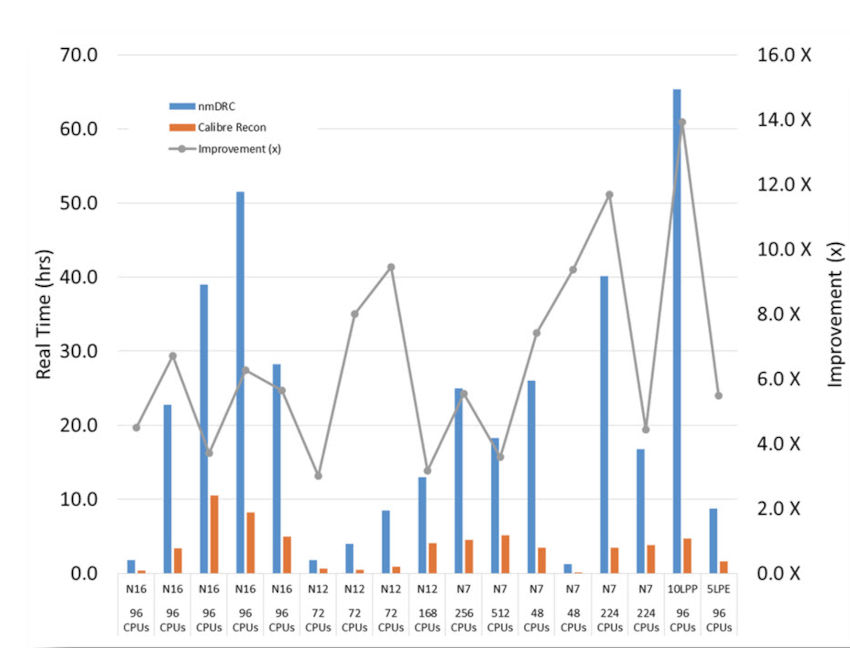
A better approach is to shift verification steps to earlier stages of the design process, significantly reducing debug time and expediting time to tape-out. Calibre nmDRC Recon is designed for early layout, whether at the IP, block, or chip level. It uses AI techniques to identify and run only those rules that are local in scope, meaning those that do not require checking across long distances or hierarchy. By focusing on local checks, Calibre nmDRC Recon significantly reduces runtime and hardware requirements.
Run time improvements using Calibre nmDRC ReconMemory Improvements using Calibre nmDRC Recon
The checks are local, so the root-cause of errors are usually close to where the errors are reported. This allows designers to quickly identify and fix system layout issues like floorplan, cell placement, or chip finishing errors. Calibre nmDRC Recon also allows designers to enable or disable certain rules or specify layers that have been changed to automatically enable all dependent rules. Identifying and fixing root-cause problems early on eliminates many individual DRC errors, further reducing the debug time.
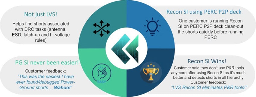
Running a subset of checks might seem counterintuitive, but it can reduce overall iteration time. The reason is that gross root-cause problems can be fixed quickly based on local checks. Rules requiring a more global scope, such as those that depend on connectivity information, can be addressed later. For these more global rules, Calibre nmLVS can help by identifying shorts early, ensuring that subsequent DRC iterations are more effective.
Using Calibre nmLVS Recon early in the flow
Full DRC checking is still necessary for final tape-out, however using techniques like split-deck runs, where checks that require significant runtime or hardware are run in parallel, overall performance can be improved. Using Calibre interactive, the individual results from each split can be combined into a single DRC results database.
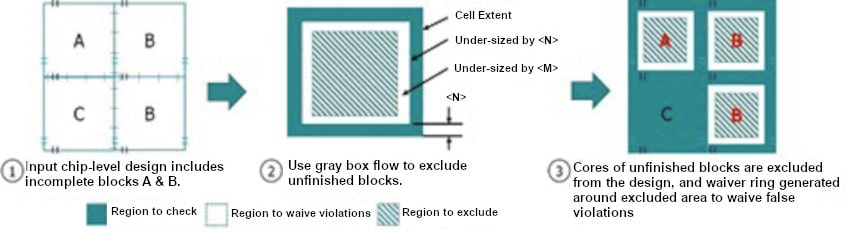
Incomplete Designs
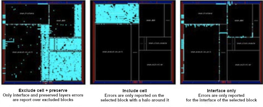
Another challenge is dealing with incomplete designs, as IP blocks of a design are not always ready at the same time. Using a combination of Calibre nmDRC Recon and Calibre nmDRC auto-waivers feature can be used. This allows designers to identify incomplete regions and exclude them from checking using markers. This “gray-boxing” technique allows designers to focus on their specific components of interest while still considering only the context of interest from clean layouts. By eliminating geometries, there is the risk of creating false errors, but the auto-waiver feature allows those errors to be removed so designers can focus on their specific component without impacting other areas of the design.
Gray-box RegionsSpecified regions
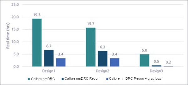
Combining Recon and auto-waivers has proven to be significantly faster than traditional methods for design layout generation and final tape-out.
Microsoft
Microsoft used Calibre nmDRC Recon to accelerate their DRC process, achieve maximum check coverage, and minimize hardware use. They started using Calibre nmDRC Recon iterations at the floorplan stage and then at the physical implementation stage. By that point, most of the designs were clean of PG shorts.
Shorter run times
Microsoft found that DRC Recon improved their early design stages, as it provided a solid foundation for pinpointing violations efficiently and significantly reduced runtimes. By adopting the shift-left approach with Calibre nmDRC Recon and auto-waivers, Microsoft was able to significantly reduce runtime, hardware requirements, and debugging time.
Conclusion
The shift-left verification strategy, using tools like Calibre nmDRC Recon is critical for addressing the challenges of complex IC designs. By focusing on local checks early, using techniques like auto-waivers, and leveraging split-deck runs, design teams can achieve faster and more efficient IC design. Microsoft showed the benefits of this approach, emphasizing the importance of adopting shift-left verification for achieving faster time-to-market.
Tell us a little bit about yourself and your company.
I am the Chief Strategy Officer at proteanTecs where I oversee our organic and inorganic growth strategies, as well as our go-to-market. This includes collaboration with ecosystem partners, defining our business model, and creating value for our customers through a targeted product portfolio. I joined proteanTecs in 2021 and have over 20 years of experience in the tech industry, big data and software domains.
proteanTecs gives advanced electronics the ability to monitor and report on their own health and performance throughout the full lifecycle. Out technology combines on-chip monitoring with a software application stack, delivering solutions for power reduction, performance optimization, and failure prevention. We offer a multi-layered, deep data and comprehensive product suite that creates a common language, breaking down data silos along the value chain and between teams.
By integrating our novel Agents (monitoring IP) into advanced semiconductor chips, our machine learning analytics and real-time applications offer unparalleled visibility – from production to the field. These deep data insights are empowering our customers in industries such as in AI, Cloud, Automotive, Telecom and Mobile to optimize their products, increasing their reliability, reducing their power consumption, and enhancing their chip and system quality. We like to say we are enabling the digital future at scale.
What was the most exciting high point of 2024 for your company?
It has been inspiring to see the results our customers have achieved. Earlier this year, we introduced proteanTecs AVS Pro™ as part of our power reduction solution. This application has enabled our customers to achieve significant power savings, leading to potential cost savings of up to $25M. One of our customers, a data center chipmaker achieved 12.5% power reduction, enabling them to increase server throughput. A mobile company saw 11.5% power savings, extending their product’s battery life. A cloud service provider was able to safely reduce power consumption by 14%. AVS Pro is a closed-loop application that performs functional-workload aware adaptive voltage scaling (AVS) in mission-mode, with a reliability protection layer. We like to call it a “safety net”. The incredible results we are seeing in customer chips really excite us, because power reduction is one of the most pressing issues and biggest limiters of scale. We have many more case studies like these across AI, networking, and other industries.
What are the biggest challenges you are seeing in the industry?
It is clear we are entering a new era of AI, which presents both new challenges and opportunities. AI is reshaping the world as we know it, AI models are getting smarter and taking on tasks we used to think only humans could perform. Because AI is spreading to a wider range of fields and applications, it is also driving the need for more powerful and efficient SoCs to handle intensive computational workloads. This trend is particularly evident not only in the surge of training processors, but also in the rise of edge AI and the increasing demand for specialized chips that can efficiently handle inference tasks. This meant our company had to adapt as well.
How is your company’s work addressing this biggest challenge?
As AI continues to evolve, the demand for powerful and efficient electronics grows exponentially. At proteanTecs, we are at the forefront, working across the ecosystem to enable companies and systems to scale reliably while meeting demanding power/performance envelopes. Consider hyperscale data centers, which house thousands of servers, all working in clusters across varying workloads. Throughput and power efficiency are vital, and TOPS per Watt becomes one of the most important metrics when evaluating new technology. That’s where our power reduction solution, AVS Pro that I mentioned earlier, is crucial. AVS Pro’s closed-loop hardware-firmware application monitors actual margin-to-timing-failure at high coverage for real-time voltage scaling. It allows precise guard-band reclamation based on actual workloads, aging, temperature, noise, and IR drops to reduce power while ensuring failure prevention.
Chip failures and performance degradation can cause significant problems, especially when dealing with the real-time processing demands of AI and mission-critical applications. In such environments, the reliability, availability, and serviceability (RAS) of systems become paramount. Introduced this year, is a cutting-edge application designed to predict and prevent failures before they happen, redefining the future of reliability.
RTHM also offers mitigation of silent data corruption (SDC), a growing challenge in high-compute environments. SDC has become a critical concern in which undetected faults propagate and lead to significant system-wide failures or computational errors, compromising data integrity. SDC is occurring at a much higher rate than software engineers expected, undermining the hardware reliability they used to take for granted. Hyperscalers, such as Google and Meta, report that approximately one in a thousand machines in their fleets is affected by SDC. RTHM enables early detection of potential failures that can lead to SDC, ensuring that systems remain resilient and reliable, even in the most demanding workloads.
What do you think the biggest growth area for 2025 will be, and why?
We are seeing more companies designing their own chips. This trend is driven by the increasing requirements of software and the desire for greater control over performance, power efficiency, supply chains, and cost. By designing their own chips, companies can optimize for specific applications, differentiate their products, and reduce reliance on external suppliers. In 2025, we foresee this trend continuing to grow rapidly. Today, we are working with the leading hyperscalers, telco players, mobile companies – all designing and developing their own chips, in addition to sourcing from the traditional big semiconductor players.
How is your company’s work addressing this growth?
Besides our offering for in-field monitoring, we also have a suite of solutions for production testing. We provide our customers with deep-data visibility to accelerate their time-to-market, enhance quality and yield, and optimize operational efficiencies. Our solutions—designed for advanced technology nodes down to 2nm—streamline the NPI process, detect latent defects, optimize performance, and enable the creation of highly customized, cutting-edge chips. With proteanTecs, customers can optimize their designs for reliability, yield, performance, and power efficiency. Our comprehensive solutions provide the monitoring IP, the EDA tools to facilitate the IP integration in the chip and ensure the implementation will provide the expected value. Once integrated we provide the ML algorithms and analytics software stack to analyze the measured data at all phases of the product cycle—from characterization, qualification, wafer testing, packaged device testing, system ramp and system test. Our solutions include edge software for inline decisions on the tester, as well as a cloud platform for advanced analytics, pinpoint debug, cross-test correlation, population analysis, and RMA investigations. Using our production analytics solutions, our customers get their products to market faster, with reduced cost, and with added confidence.
What conferences did you attend in 2024 and how was the traffic?
In 2024, proteanTecs participated in many events and conferences in the automotive, data center and semiconductor industries. These events spanned the globe—with our team participating in shows in the United States, Spain, Germany, Belgium, Portugal, the United Kingdom, the Netherlands, Israel, Japan, China, Taiwan, Korea, and India.
We participated in events similar to prior years, but also added some new ones to our calendar, especially in Japan as we expanded our strategic focus there. Of note, we kicked off 2024 with a strong presence at Automotive World in Tokyo, where we also co-hosted an Exclusive Tech Summit with Advantest with hundreds of guests, and guest speakers from Renesas and NTT.
Events with our ecosystem partners continue to be a big focus. We participated in partner events with TSMC, Intel Foundry, Samsung Foundry, Teradyne, PDF Solutions and Cadence. We also ramped up our presence at the annual Design Automation Conference (DAC). Our proteanTecs booth featured in-booth demos, along with presentations from several ecosystem partners, including TSMC, GUC, Siemens, Intel Foundry, UCIe, Teradyne and Andes Technology.
Events have clearly rebounded since COVID-19. We consistently saw strong booth traffic across our different global events. Attendees are also eager to experience, firsthand, our interactive live product demos, based on customer systems.
Will you attend conferences in 2025? Same or more?
Absolutely. In fact, our 2025 event calendar is filling up quickly. We are committed to participating in industry events and strengthening relationships through in-person connection. A big part of our strategy is centered around on-stage talks, and we plan to be many relevant venues again this year.
Throughout 2025, we look forward to collaborating across the ecosystem, presenting new solutions to technical challenges, exploring new business opportunities, and contributing to more data-driven decisions across the industry.
How do customers engage with your company?
Customers can engage with proteanTecs in a variety of ways. With a global team working across seven locations worldwide, we provide our customers with exceptional support on-site with our dedicated application engineering team, and provide them with everything they need to maximize their value from the insights they generate using our solutions.
We encourage interested parties to contact our team to book a customized product demo or ask any technical questions. They can also visit our website to explore a wide range of materials in our knowledge center, including white papers, case studies, on-demand webinars, and other informative content. Following us on social media, particularly LinkedIn, is an excellent way to stay updated on our latest news and industry insights. Last, but certainly not least, you can connect with our team at upcoming industry events and conferences.
Additional questions or final comments?
proteanTecs celebrated its 7th anniversary this year. It’s been an incredible journey marked by significant milestones. Throughout 2024, we introduced three new solutions—Power Reduction, RTHM™ (Real-Time Health Monitoring) and RTSM™ (Real-Time Safety Monitoring). We signed new customers across multiple industries, we also announced strategic partnerships, including a collaboration with Alphawave Semi and our participation in Arm Total Design. These achievements are a testament to the hard work and dedication of our talented team, along with the trust of our customers. Stay tuned for what we have in store during 2025, we are going to share some exciting updates soon!
Multi-die design has become the center of a lot of conversation lately. The ability to integrate multiple heterogeneous devices into a single package has changed the semiconductor landscape, permanently. This technology has opened a path for continued Moore’s Law scaling at the system level. What comes next will truly be exciting. Before getting too excited it’s important to realize there are still substantial challenges presented by this new method of system design.
These challenges are interrelated and span from architectural all the way to manufacturing and deployment in the field. Solving these problems is a multi-dimensional balancing act. A holistic approach is the only effective strategy. The problem is actually broader than multi-die design. It also includes new communication strategies, new materials, new thermal and mechanical problems among others. The term heterogeneous integration is more accurate. There are few companies with the breadth and depth of capability to tackle this class of problem. Synopsys is one of those companies and they have taken a unique approach. I examined some aspects of the Synopsys solution in a recent post. Let’s go deeper and examine what is different about Synopsys’ comprehensive, scalable solution for fast heterogeneous integration.
Early Architecture
The graphic at the top of this post presents a good overview of the multi-dimensional nature of heterogeneous integration. It turns out Synopsys has published a series of white papers that cover the full spectrum of the problem. Taken together, this material presents all the elements of a master class on the topic. I highly recommend taking the time to read them all. Links are coming. Let’s first take a quick look at what each white paper offers. I’ll start with the early architecture topics.
This first white paper begins with an overview of the various tasks that must be considered to achieve a successful multi-die design project. Those items are summarized in the figure below.
Multi die system design challenges
This white paper focuses on system pathfinding, memory utilization & coherency, and power/thermal management. A key to successful multi-die design is a virtual prototyping environment for early architecture exploration. This environment allows architects to capture the hardware resources of their multi-die design. The architecture of such a system is described.
Key items that are analyzed and balanced here include workload and architecture definition, partitioning and technology selection, and early performance and power analysis. The Synopsys Platform Architect for Multi-Die is described, which addresses all these requirements and more.
System Verification and Validation
The next white paper discusses the challenges of verification and validation for multi-die designs. Areas of focus here include addressing capacity and performance for system verification, validating assumptions made during architecture design, and knowing when verification is complete. Simulation and emulation models must be able to scale with the design size and make best use of the available resources. It is also important to consider analog components, which must either be modeled digitally or co-simulated in a mixed-signal environment.
The white paper goes on to point out that the key to addressing the challenges outlined above is recognizing that a multi-die design is not a single design, but rather a combination of independently manufactured designs (dies) interconnected through communication fabrics. The figure below provides a disaggregation example, showing how a monolithic design becomes a combination of dies, creating numerous verification challenges.
Example of disaggregation that affects verification
It is explained that, to perform system-level tests, the RTL designs for all the dies must be assembled and simulated in a single executable. This presents many challenges, including:
How can “independent” designs and testbenches be assembled into one simulation environment?
Can the die-level testbenches be reused or synchronized?
Does the compute server have enough memory to build and execute the simulation?
Can the simulation be distributed over multiple servers?
How can name clashes be avoided?
The paper goes on to describe the Synopsys VCS® functional verification solution, that provides a powerful and flexible approach to multi-die design simulation. Details of how NVIDIA used this capability on a real design are also provided.
Design Implementation and Signoff
Next, we examine the challenges of implementation and signoff. This white paper discusses the challenges faced here, which include signoff for multi-die extraction and timing, multi-die power, and multi-die physical design.
The white paper explains that multi-die signoff is impossible with traditional 2D timing, checking, and power analysis tools. For example, signals that cross between dies pass through multiple stacked layers, including interposers and substrates, and the delays through these layers must be considered for static timing analysis. This places new requirements on both physical verification and parasitic extraction.
In addition, power calculations are more complex since they must combine the results for all dies. Multi-die design also requires innovation for design rule checking (DRC), layout versus schematic (LVS) verification, and other physical checks. The reality is that accurate multi-die signoff requires the entire stack to be considered in a holistic way.
The paper describes the suite of tools Synopsys provides to address these challenges in an integrated and unified way. The figure below summarizes the technologies discussed.
Synopsys multi die signoff solution
Silicon IP Integration
This white paper examines the challenges of efficient multi-die design implementation and IP integration. UCIe, as a specification for die-to-die interconnect is discussed. The complexities of a multi-die package with UCIe expressing die-to-die connectivity are reviewed.
An example shows one UCIe link on the I/O chiplet (Die 1) being connected through the package with the other UCIe link on the CPU/compute die (Die 2). The UCIe link consists of a physical layer (PHY) and a controller. The UCIe PHY includes the transmit/receive (TX/ RX) pins, which must be routed through the package to the UCIe PHY on the other die. The UCIe PHY IP is composed of 8 DWORDs, is placed in a row next to each other. Each DWORD consists of a pair of clocks, 64 single-ended data lanes, a data valid lane in each direction (transmit and receive), and a track lane. Additionally, there is a low-speed sideband bus for initialization, link training, and configuration read writes.
The diagram below illustrates this configuration.
Die 1 to Die 2 connectivity for UCIe
This white paper goes into the details of how the combination of Synopsys UCIe IP and Synopsys 3DIC Compiler enable higher productivity with lower IP integration risk by automating routing, interposer studies, and signal integrity analysis. There’s a lot to consider here, both in terms of IP choices for communication and implementation of complex interconnect schemes. You will get a good appreciation of the completeness of the Synopsys solution.
Manufacturing and Device Health
The final white paper discusses effective monitoring, test, and repair of multi-die designs. The piece points out that multi-die designs are more costly to build and test than traditional single-die packages. Only one failed die in a multi-die configuration can cause the entire system to fail. Thus, the quality of each die and the integrity of the interconnect is critical.
This white paper goes into significant detail regarding the array of Synopsys solutions to cover test, repair and device health through its lifetime. It also explains how Synopsys IP is integrated into the chip design to implement these capabilities.
HBM is a popular standard for integrated memory in multi-die designs. The standard defines an interface for 3D-stacked synchronous dynamic random-access memory (DRAM) dies. It specifies the PHY-level logic-to-memory interconnection. The white paper describes how Synopsys SLM SMS ext-RAM IP supports at-speed interconnect test and diagnosis of memory dies as well as post package repair (PPR).
This IP provides:
Comprehensive at-speed interface and memory array testing and diagnosis
Programmable test algorithms, address types and ranges, test operation time, and DRAM access timing
Diagnostics data reporting
Memory fault type and failing address/data lanes
Post-packaging repair via HBM stack repair signature
The figure below shows how the pieces fit together.
Synopsys SLM SMS ext RAM IP for memory test and repair
To Learn More
This is just a high-level summary of the broad coverage Synopsys offers for multi-die design and heterogeneous integration. The white papers mentioned provide substantially more detail. If a multi-die design is in your future, you will find this material to be quite valuable. Here is where you can get your own copies:
This information will help you better understand what is different about Synopsys’ comprehensive, scalable solution for fast heterogeneous integration.
Tell us a little bit about yourself and your company, AMIQ EDA.
We are an EDA company providing software tools targeting both chip design and chip verification. Our tools enable engineers to increase the speed and quality of new code development, simplify debugging and legacy code maintenance, accelerate language and methodology learning, improve testbench reliability, extract automatically accurate documentation, and implement best coding practices.
What was the most exciting high point of 2024 for your company?
Our most exciting innovation for the year was our first incorporation of artificial intelligence (AI) Into our products. As Serban Ionica discussed in October, AI Assistant is included for no extra cost in the latest releases of DVT IDE for Visual Studio (VS) Code and DVT Eclipse IDE. It works with any large language model (LLM) to generate new design or verification code and to explain and improve existing code. The results are much better than with a general-purpose AI tool because we leverage our project database and its deep knowledge about your design and testbench. Users are telling us that we have really improved their coding and debug efficiency.
What was the biggest challenge your company faced in 2024?
Two of the challenges I mentioned last year continue as our company and user base continue to grow. Of course, growth is good, but it does make it harder to provide rapid and accurate customer support and to hire enough of the best people to evolve our products and develop new ones.
How is your company’s work addressing this biggest challenge?
I believe that AI Assistant helps with customer support, since it enables users to ask questions about their code in natural language. The more intuitive the user interface, the fewer questions users have to ask. We continue to create very popular “how to” videos and we have started a new series of posts on common pitfalls in SystemVerilog. As for hiring, the internship program I mentioned last year has been an incredible success. It takes a lot of time and effort to make it work so well, but many of our interns join us full time when they graduate and are productive from the first day. We also recruit through job fairs and social media, but the internship program is our largest and best source for new employees.
What do you think the biggest growth area for 2025 will be, and why?
We are seeing a big upturn in VS Code interest among users. We are also seeing increased usage for our Verissimo SystemVerilog Linter and Specador documentation generator. I certainly expect AI to be a growth area as well. AI Assistant is getting more capable all the time, and we’ll be applying AI wherever we can to improve our entire product line.
How is your company’s work addressing this growth?
Of course, we’re always adding new features to all our products. For example, our DVT IDE family now smoothly handles preprocessor code, even when it’s in a proprietary language. Also, we’ve added more than 70 new rules to Verissimo over the past year. On the AI side, we work with domain experts to educate our team and ensure that we’re using all the latest relevant tools and technologies.
What conferences did you attend in 2024 and how was the traffic?
We attended and exhibited at our usual in-person events: the Design Automation Conference (DAC) in the U.S. and the Design and Verification Conference (DVCon) in the U.S. and Europe. Traffic was better than last year, showing that engineers are comfortable traveling to conferences again and that their companies have the budget to send them. We also attended Open Community Experience (OCX), the Eclipse Foundation’s flagship developer conference. We heard about a lot of interesting topics in the open source community, from IDEs of the future to cyber resilience.
Will you attend conferences in 2025? Same or more?
We expect even better traffic this year, so we plan to attend the same three events. We always enjoy catching up with users, friends, and colleagues while seeing some new faces as well.
Additional questions or final comments?
I said a year ago that 2024 should be another outstanding year for us, and indeed it was. I fully expect the same for 2025. We’ll continue to provide regular updates to SemiWiki on what’s happening at AMIQ EDA. Thank you for your time.
Daniel Nenni is joined by Dr. Sailesh Kumar, CEO of Baya Systems. With over two decades of experience, Sailesh is a seasoned expert in SoC, fabric, I/O, memory architecture, and algorithms. Previously, Sailesh founded NetSpeed Systems and served as its Chief Technology Officer until its successful acquisition by Intel. Sailesh is also a prolific author, with more than two dozen highly cited papers and over 150 patents.
Dan covers a lot of ground in this far-reaching discussion with Sailesh. The ways AI is disrupting computing architectures are explored, with a focus on the new requirements for high-performance data movement. The various standards under development to improve external interfaces and implement chiplet-based design are also explored. Dan also discusses the recent announcements from DeepSeek with Sailesh, who comments on the significance of the work and the likely impact on the industry going forward.
Sailesh also provides an overview of the unique design platform offered by Baya Systems that helps to tame the complexity of next generation design. Sailesh also comments on the importance of relationships when building a new technology company and the “network effect” that is present in Silicon Valley.
The views, thoughts, and opinions expressed in these podcasts belong solely to the speaker, and not to the speaker’s employer, organization, committee or any other group or individual.
Fabrizio Del Maffeo is the CEO and co-founder of Axelera AI, the Netherlands-based startup building game-changing, scalable hardware for AI at the edge. Axelera AI was incubated by the Bitfury Group, a globally recognised emerging technologies company, where Fabrizio previously served as Head of AI. In his role at Axelera AI, Fabriozo leads a world-class executive team, board of directors and advisors from top AI Fortune 500 companies.
Tell us about your company?
Axelera AI was founded in July 2021 with Evangelos Eleftheriou, emeritus IBM Fellow, myself and a core team from Bitfury AI, IMEC, researchers from IBM Zurich Lab, ETH Zurich, Google and Qualcomm.
Our mission is to rapidly provide access to advanced Edge AI-native hardware and software solutions for companies of all sizes across a range of market verticals and place AI in the hands of those who could not otherwise afford it. We do this by delivering faster, more efficient and easy-to-use inference acceleration while minimizing power and cost. To do this, our platform is purpose-built to support AI strategies across a wide-range of industries while seamlessly integrating with existing technologies.
With our team of brilliant engineers, developers and business experts, we are focused on building our solutions and ecosystem that together will drive the democratization of AI, enabling a green, fair and safe world.
In three years, Axelera AI has raised USD 120 million, built a world-class team of 190+ employees (including 60+ PhD’s with 40,000+ citations), launched its Metis™ AI Platform and is the largest AI semiconductor company in Europe.
The company is backed by major institutional investors, including Samsung Catalyst Fund, the European Innovation Council Fund, Innovation Industries Strategic Partnership Fund (backed by MN/Pension Fund for Metal and Technique), Invest-NL Deep-Tech Fund , along long-standing investors Verve Ventures, Innovation Industries, Fractionelera, the Italian sovereign fund CDP Venture Capital SGR, the Dutch Enterprise Agency (RVO), Bitfury, Federal Holding and Investment Company of Belgium (SFPIM), imec andimec.xpand.
What problems are you solving?
Current iterations of AI technology have leveraged more general purpose acceleration and have delivered expensive, power-hungry solutions that prove to be inefficient for many use cases. In the cloud, with access to water-cooling and large power supplies, this architecture suffices, but it is poorly suited for the edge.
At Axelera AI, we are revolutionizing the field of artificial intelligence by developing an industry-defining hardware and software platform for accelerating computer vision and generative AI on edge devices. Our platform, built using proprietary in-memory computing technology and RISC-V dataflow architecture, delivers industry-leading performance and usability at a fraction of the cost and energy consumption of current solutions.
Power consumption is a critical factor both on devices and in data centers. Axelera AI offers leading compute density with exceptional core efficiency which means systems can easily crunch data without draining power or running hot, with a typical use case requiring just a few watts.
One of the biggest challenges for Edge AI is optimizing neural networks to run efficiently when ported onto a mixed-precision accelerator solution. Our platform includes advanced quantization techniques and mapping tools that significantly reduce the inference computational load and increase energy efficiency. By creating integrated solutions that are powerful, cost effective and efficient, Axelera is bringing inference to the edge with accuracy.
What application areas are your strongest?
Axelera AI is primarily focused on providing powerful AI inference solutions for edge computing and high-performance applications. The first generation of AI processing unit, Metis, focuses on primarly on computer vision and some of the strongest application areas include:
Security and Surveillance Axelera AI excels in real-time image and video processing for applications like campus management, safety, surveillance, access control
Automotive: autonomous vehicles and infotainment
Industrial automation: real-time high speed quality control, pick-and-place and general purpose robotics
IoT Devices: Their technology is well-suited for IoT applications, enabling smart devices to process data locally with minimal latency.
Smart Cities: AI-powered analytics for traffic management, public safety, and resource optimization can benefit from Axelera’s capabilities.
Retail: Providing a frictionless experience for customers with personalized recommendations, queue management, fast and efficient checkouts, and smart mirrors.
Healthcare: With nearly 10 million fewer health workers[1] than the world needs, bringing AI inference to the healthcare system will allow doctors to more quickly understand and diagnose patients.
We have been working on broadening our future product offerings from the edge to the enterprise servers to address the growing computing needs for generative AI, large language models and large multi-modal models.
What keeps your customers up at night?
Neural networks are getting bigger and they require more computations. Scaling performance using CPUs and GPUs are inefficient and extremely expensive. We are fully focused on tailoring our technology around the new emerging needs, efficiently offloading completely the AI acceleration from the CPU inside our AI processing unit.
We must also contend with the realities of the current chip market. These realities include the high cost of hardware, as well as ongoing shortages in the industry. A discrepancy in the demand and supply of chips, fueled by supply chain delays, the pandemic, natural disasters and labor market changes, is heavily impacting the global semiconductor space.
There is also the question of Moore’s Law and energy usage. Moore’s Law suggests that the number of transistors in an integrated circuit would double every two years, which played a driving role in modern tech development like computers. However, modern semiconductors are far more technologically complex and require significant energy to produce and progress. With our Metis AI Platform, we aim to overcome these challenges by delivering a product that packs the power of an entire AI server – all at a fraction of power consumption and cost of other solutions.
What does the competitive landscape look like and how do you differentiate?
Until now, AI systems and applications have relied on the computational performance of large, power hungry and expensive hardware. However, fully unlocking the potential of AI, especially at the Edge, requires a dramatic increase in FPS/$ which will enable complex AI applications to run on-device at the Edge. Running the industry-standard benchmark of ResNet, YoloSSD-Mobilenet families, the Metis PCI delivers high performance at a fraction of power consumption and price of today solutions. Furthermore, Metis excel in real application pipelines thanks to the possibility to run in parallel on different core multiple networks, delivering 5-10x higher throughput than existing solutions.
A major advantage of our SRAM-based D-IMC technology is that it has been implemented in standard CMOS technology. Our design uses proven, cost-effective and standard manufacturing processes, readily available in any silicon foundry which brings supply chain resiliency to system builders. Memory technologies are also a key driver for lower lithography nodes. So, Axelera AI will be able to easily scale performance as the semiconductor industry brings advanced lithography nodes into volume production.
We are also going beyond just the accelerator technology and chip development, building a fully interconnected ecosystem of support powered by a versatile and easy-to-use software stack: our VoyagerTM SDK.
What new features/technology are you working on?
The full production-ready Metis AI platform is now in production delivering high performance and preserving 99% of the original model’s precision, indistinguishable from GPU-based inference models, while offering 4-5 times throughput, energy efficiency and cost savings.
We have a complete product portfolio including standard form factors like an M.2 card to PCI-E cards capable of handling the most demanding vision applications. We have a complete roadmap that scales from single digit watt usage to enterprise grade server usage.
Our platform includes advanced quantization techniques that enable customers to run out of the box state of arts neural networks and mapping tools that significantly reduce AI computational load and increase energy efficiency,
Finally, our software tool chain allows customers to build up a complete application pipeline in a matter of minutes, simplifying the deployment of artificial intelligence in any device and opening up unprecedented opportunities for mass deployment of AI solutions.
Nowadays we are working on expanding the neural networks zoo to support Large Language Models on Metis. We are also in advanced design with the new AI processing unit, complementary to Metis and more focused on generative AI workload. The product line will be announced later next year.
How do customers normally engage with your company?
Whether you are a computer vision system developer or integrator, software vendor or OEM, our AI acceleration hardware has been built to meet your needs. Delivering leading AI acceleration hardware in a range of industry accepted form factors supported by our easy-to-use software stack, Metis simplifies development, integration and deployment of AI inference acceleration.
Valuation kits are available in six variations, each designed for industry-defining AI vision inference. The kits are equipped with the Metis AIPU integrated in an AI Acceleration card, and the Voyager Software Development Kit, allowing users to evaluation performance and vision systems using popular AI inference networks such as YOLOv7.
Customers use the SDK to bring their applications into the Metis AI platform and run it on Axelera’s powerful Metis AI Processing Unit (AIPU), whether the application is developed using proprietary or standard industry models. The VoyagerTM SDK offers end-to-end integration and is API-compatible with de-facto industry standards, unleashing the potential of the Metis AIPU, delivering high-performance AI that can be deployed quickly and easily.
The VoyagerTM SDK comes with a Model Zoo, a catalog of state-of-the-art AI models and turnkey pipelines for real-world use cases including image classification, object detection, segmentation, keypoint detection, face recognition and other Computer Vision tasks. Importantly, developers can easily modify any of the offered models to work with their own datasets or make them fit better to their application requirements.
We are working on creating a frictionless experience for our customers who soon will be able to buy online our products and get supported by an online developer community.


