Paul Wells, CEO at sureCore, an ultra-low power memory specialist, has been involved in the semiconductor industry for over 35 years. Previously, he has worked as Director of Engineering for Pace Networks where he led a multidisciplinary product development team creating a broadcast quality video and data mini-headend. Before this, he worked for Jennic Ltd as VP Operations, successfully building the team from scratch as the company transitioned to a fabless model. Prior to this, he was responsible for a team at Fujitsu Microelectronics supporting ASIC customers in Europe and Israel.
Tell us a little bit about yourself and your company.
I’ve been in the semiconductor industry now for over 35 years. I began my career at Ferranti Electronics in Manchester, UK, as an ASIC engineer delivering custom chips for a wide range of innovative consumer applications. Ferranti had invented the gate array and the possibilities for its use seemed endless. I also worked for Fujitsu, Jennic and Pace Networks, holding senior engineering and operations positions, before co-founding sureCore and taking on the role of CEO back in 2011.
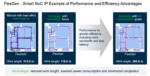
SureCore started out by taking a radically different view of memory. All SoC devices need embedded memory, usually SRAM, but also register files, and occasionally ROM. With the growing trend to even more integration, and the need to be able to accommodate larger software footprints, the demand for on-chip memory just kept increasing until for some devices it reached 70% die area! SRAM whilst fast is also power hungry and by analysing the traditional architectures we were able to identify some key power saving strategies that resulted in up to 50% dynamic power savings.
For many consumer and medical products, the performance delivered by modern process nodes is often overkill. Very significant power savings can be achieved by operating at much lower voltages and sureCore have been able to develop and demonstrate in silicon the industry’s lowest operating voltage SRAM. These power optimising technologies are embedded in our market-leading PowerMiserTM and EverOnTM product families. By exploiting our ultra-low power design expertise, we have created our sureFITTM custom memory development service that provides our customers with the optimal solution for their application.
What was the most exciting high point of 2024 for your company?
Throughout 2024 sureCore delivered a number of custom advanced memory implementations, including a low power memory compiler for 16nm FinFET.
SureCore also continued to lead on the cutting-edge government funded InnovateUK project to develop cryogenic IP for quantum computers. We successfully taped-out a cryogenic IP demonstrator – our test chip which included cryogenic SRAM, register files and ROM based on the GlobalFoundries 22FDX process. As part of the seven member consortium transistor parameters were measured at both 77K and 4K, and SPICE models updated using advanced TCAD. We received samples in November and the great news is that the devices are working extremely well. We already have a lead customer who has proven that the IP works at 3.3K and we just need to complete the full chip characterisation to fully validate the compiler space.
What was the biggest challenge your company faced in 2024?
After a buoyant 2022, 2023 and early 2024 presented very challenging market conditions for the semiconductor industry. Geopolitical issues and the ever increasing importance of semiconductors to the global economy turned out to be a double-edged sword, with restrictions being imposed on advanced manufacturing equipment sales whilst the Chips Acts in both Europe and the US pumped money into the industry. However, this funding seems so far to have done little to stimulate the sector. Despite these challenges, sureCore have managed to successfully navigate the downturn. In fact, we saw an upsurge in business, especially our specialist design services, in the third and fourth quarters.
How is your company’s work addressing this biggest challenge?
SureCore’s ultra-low power memory solutions can provide our customers with a competitive advantage in the market. Battery powered products in particular continue to evolve, with Edge AI applications, smart watches and health monitors pushing the boundaries of what is possible in small form factor devices. With the upturn in the 2nd half of 2024 and extending into 2025 we are now seeing increased interest in how our novel power saving technology can help developers meet their ever tightening power budgets. We have global representation and continue to attract new customers from across Asia, the US and Europe.
What do you think the industry’s biggest growth areas will be in 2025?
Unfortunately, the outlook for the global economy is still not very encouraging. However, the current enthusiasm for AI continues unabated and this will almost certainly be the big growth driver in the semiconductor industry in 2025. Edge AI is likely to progress if only as a way to offload some of the pressure on data centres. We also believe that smart medical and healthcare solutions will gain further traction as the baby boomer generation starts to really focus not just on ‘life-span’ but on ‘health-span’ extension.
What about industry conferences and events?
Last year we prioritised the foundry events, attending TSMC Technology Symposiums and OIP events, in addition to the GF Technology Summits. As usual these events were well attended and provided excellent networking opportunities. In 2025, we plan to attend several industry events – certainly the foundry events. We are also looking at Embedded World and DAC.
What will be the main product focus areas for your company in 2025?
The sureCore team will continue to innovate in the ultra-low power memory market, addressing the key issues of both dynamic and leakage power. The cost-effectiveness of both 16nm and 12nm technologies is becoming a key focus for us as product companies are increasingly recognising their benefits. We are also working with lead customers down to 4nm and it is encouraging that our power saving technology seems to migrate well to these more advanced nodes. In addition, although the quantum computing market is still in its infancy, we will continue to push our cryogenic design expertise and engage with as many companies in this sector as possible. 2025 looks set to be another exciting year for sureCore, with many interesting customer projects and deliveries in the pipeline – so watch this space!
Also Read:
sureCore Brings 16nm FinFET to Mainstream Use With a New Memory Compiler