RVN! 26 Banner revised (800 x 100 px) (600 x 100 px)

STM FD-SOI Manufacturing Double Source: Samsung

STM FD-SOI Manufacturing Double Source: Samsung
by Eric Esteve on 05-15-2014 at 8:54 am

Let’s start with apologies: when guessing that SMIC would be the 2[SUP]nd[/SUP] source foundry for ST-Microelectronics 28nm FD-SOI, I was wrong. To be honest, if I had made the assumption that Samsung was this double source, I would have generated dozen of comments, calling me “crazy blogger”…for the best. Announcing Samsung as the first FD-SOI foundry partner is certainly one of the best deal that STM could make. According with private talk that I recently had when trying to know the name of this foundry, there will be other licensing agreement signed, and we can guess that SMIC is still a potential partner. Let’s have a (semiconductor) dream: TSMC could be another STM partner, and support FD-SOI!

Just a reminder, this comment made in Semiwiki a couple of weeks ago:

I really think that FD-SOI is a great technology, which can be used to fab chips at a lower cost, or at lower power-or higher performance- for the same cost. The magic is that you can gain one technology node, like stay in 28nm, but with the power or performance benefit of 20nm.
But, in the real life, to attract customers, you need to open two doors:

  • Wafer double sourcing
  • Manufacturing double sourcing

Each of these point can be a show stopper. Let’s assume that SOITEC and STMicroelectronics are working these business issues, then the next issue is to develop a large enough ecosystem around IP and EDA. This is more like a chicken and egg issue, but, as soon as the right amount of money will have been invested to make sure that the right IP are available, the design-win will generate enough cash will be invested to enlarge the ecosystem. This is not as magic as the technology, it’s just a question of business decision, strategy planning and business development!

  • SOI Wafer double sourcing: ticked since October 2012

I had a fruitful discussion today with Paul Boudre, COO of Soitec, and Christophe Malleville, in charge of the Electronic BU with Soitec. At first, they have confirmed information that anybody could find in the web, the 10 years license agreement signed in October 2012 with Shin-Etsu Handotai Co., Ltd (SEH), the world leader in the manufacturing of silicon wafers. Just an extract of the related PR: “We are very excited about the business opportunities for SOI products, and we look forward to working with Soitec to extend the global supply chain for new products, such as FD-SOI and SOI for FinFETs, which are showing potential benefits in mobile and embedded applications,” said Nobuo Katsuoka, SEH director, SOI process engineering department. According with Paul Bourde, FD-SOI target market is a mass market. The forecast for Silicon wafer in production in 2017 to support 28nm technologies is 4 to 5 million wafers, out of these, up to 25% -or above 1 million- are expected to be SOI wafers.

  • Manufacturing double sourcing: ticked since yesterday!

Just listen to STMicroelectronics: “Building upon the existing solid relationship between ST and Samsung within the framework of the International Semiconductor Development Alliance, this agreement further strengthens our cooperation by extending it to 28nm FD-SOI, while expanding the ecosystem and augmenting fab capacity for ST and the entire electronics industry. Moreover, the agreement confirms and strengthens further the business momentum that we have experienced on this technology during the past quarters through many customers and project engagements in our Embedded Processing Solutions segment” said Jean-Marc Chery, Chief Operating Officer, STMicroelectronics. “We foresee further expansion of the 28nm FD-SOI ecosystem, to include the leading EDA and IP suppliers, which will enrich the IP catalog available for 28nm FD-SOI.” On top of this very important announcement, the key-word from this message is “ecosystem”.

This Samsung-STMicroelectronics partnership applies to manufacturing, but it also encompasses Design Kit. According with this presentation, the licensing deal includes:

  • Samsung is licensing the 28nm FD-SOI design platform (Process Design Kit (PDK), foundation libraries, advanced IP, design flow)
  • Samsung and ST will support common 28nm FD-SOI library and IP
  • The PDK is available now so customers can design immediately.

If you take a deep look at the above picture (and read between the lines), you then realize that STM keeps a certain competitive advantage, at least for now, as the deal does NOT includes:

  • ADC/DAC
  • High Speed links (USBPHY, HDMI, MIPI D-PHY, M-PHY)
  • Memory Controller PHY: DDR3/4, LPDDR3/4, etc.
  • Very High Speed links: PCIe gen-3, SATA3, USB 3.0, 3.1, etc.

If we except ADC/DAC, these analog mixed-signal IP are 100% within the radar of IPNEST (see this survey): these are now the real IP differentiators (if we consider that ARM CPU, IMG GPU or CEVA DSP are equally available to every SoC design teams). STMicroelectronics has a long history with PHY IP development, initially to support in-house SoC design, then to support STM foundry customers. But, if you look at the customers targeted by the 28nm FD-SOI technology, a large proportion expect to externally source these high end IP (like they do when using TSMC foundry). What does that means? Just that this 2[SUP]nd[/SUP] source announcement is the starter for another race: the development, or porting, of high end IP on 28nm FD-SOI technology. Nobody may argue anymore that 28nm FD-SOI is a niche technology. IP vendors should now being motivated, as FD-SOI will be a real market generating additional licensing revenues. Developing High End IP will help creating this ecosystem which is the last condition for FD-SOI success in the semiconductor industry…

From Eric Esteve from IPNEST

More Articles by Eric Esteve…..

lang: en_US


Atmel and the Arduino Zero

Atmel and the Arduino Zero
by Paul McLellan on 05-15-2014 at 7:00 am

As I wrote about last month, this weekend is the Maker Faire in San Mateo. If you are interested in the cutting edge of what people are getting up to outside of the corporate world, this is the place to go. You will see stuff that you will not hear about for a year or two when it finally goes mainstream.

Increasingly, there is a lot of electronics at the center of things. Obviously a 3D printer, for example, needs a microprocessor. It turns out that over 90% of 3D printers are powered by Atmel.

Another famous name in the maker community is Arduino. This is an open-source platform for building very low cost (think $10) systems. Today, Atmel and Arduino announced the Arduino Zero, a new board focused on what might be required for the internet of things (IoT), wearables and so on. It is higher performance than the Arduino UNO. It is also powered by an ARM M0.Arduino Zero is a simple, elegant and powerful 32-bit extension of the platform. The Zero board aims to provide creative individuals with the potential to realize truly innovative ideas for smart IoT devices, wearable technology, high-tech automation, robotics and projects not yet imagined. The board is powered by Atmel’s SAMD21 MCU, which features a 32-bit ARM Cortex M0+ core.

Some technical details:

  • the Arduino Zero board features the Atmel SAMD21 Microcontroller
  • with 256kb of flash
  • 32kb SRAM
  • TQFP package
  • Compatible with 3.3V Shield that conform to the Arduino R3 Layout
  • development with the Arduino Zero using the Arduino programming language

The Arduino Zero board also features flexible peripherals and Atmel’s Embedded Debugger (EDBG), which provides a full debug interface on the SAMD21 without the need for additional hardware, significantly increasing the ease-of-use for software debugging. EDBG also supports a virtual COM port that can be used for device programming and traditional Arduino boot loader functionality.

The first prototypes of the Arduino Zero will be on display at the Maker Faire Bay Areay 2014 in San Mateo on:

  • Ardiuno booth 204
  • Atmel booth 205
  • ARM booth 405

Go and check them out.


Apache Design @ #51DAC Must See!

Apache Design @ #51DAC Must See!
by Daniel Nenni on 05-14-2014 at 8:00 pm

Register to hear industry experts from top semiconductor companies share their best practices that enable the next generation of high-performance, low power designs for mobile, automotive and other applications. Meet our technologists for in-depth presentations, case studies and demos on the industry’s leading simulation platforms for power, noise, thermal, EMI and reliability integrity sign-off from RTL to silicon, across chip, board, and system.

Design experts from the following Mobile, IoT and Automotive Electronics companies will be sharing their experiences with ANSYS and Apache tools in our suite. Space is limitedso register now to reserve your spot:

  • Applied Micro: System Power Analysis with Correlation Results for Advanced Processor Designs – 1:00PM, Tuesday, June 3
  • Ciena: Power Analysis using PowerArtist for WaveLogic3 ASIC, a Third Generation 100Gbs Coherent Metro Optical Modem – 12:00PM, Monday, June 2
  • LSI: Silicon Correlation of RedHawk Dynamic Voltage Drop in High Power SoC for Storage Application – 1:00PM, Wednesday, June 4
  • NXP: Noise Coupling Analysis for Advanced Mixed-signal Automotive ICs – 3:00PM, Tuesday, June 3
  • Samsung: Chip-Package-System based Power Integrity Analysis Flow for 14nm Mobile Designs – 1:00PM, Monday, June 2
  • STMicroelectronics: Designing Smart Power-Grid with Reduced Die-Area Using RedHawk – 12:00PM, Wednesday, June 4
  • Synapse: Designing Wireless Systems for Wearable Electronics and Internet of Things – 2:00PM, Monday, June 2

Click REGISTERto see one or more of these presentations at ANSYS suite.

Products and Technologies

Check out the 30+ in-depth technical presentations and demos from our key technologists. These sessions focus on your top design challenges including consistent power reduction, FinFET based design sign-off, EM/ESD and thermal reliability, chip-package-system convergence, system modeling and more.

Click REGISTERto reserve your seat today.

Fun and Informational Activities
Explore ANSYS and Apache product offerings for mobile, IoT and automotive applications using the touch screen demo kiosk.Enjoy the video,Apache Past, Present and Future, and hear what inspires Apache’s founding team.Play the game, Life of an Engineer, and win fun prizes.

lang: en_US


Synopsys @ #51DAC Must See!

Synopsys @ #51DAC Must See!
by Daniel Nenni on 05-14-2014 at 11:00 am

Accelerating Innovation—that has been at the heart of Synopsys’ commitment to its customers for more than 25 years. As a leader in EDA and semiconductor IP, Synopsys’ software, IP and services help engineers address their design, verification, system and manufacturing challenges and accelerate their innovations. Since 1986, engineers around the world have used Synopsys technology to design and create billions of chips and systems. What will you design next? Visit Synopsys at Booth #1133 to learn more about the newest solutions available to help you to accelerate your innovations.


Special Events
Register early for these Synopsys events at DAC. View an event below for more information and to reserve your place:
[TABLE] cellpadding=”1″ style=”width: 650px”
|-
| [TABLE] cellpadding=”2″ cellspacing=”1″ style=”width: 100%”
|-
| valign=”top” | June 2
| valign=”top” | Samsung/Synopsys Breakfast
|-
| valign=”top” | June 2
| valign=”top” | IC Compiler/IC Compiler II Lunch: Addressing Advanced Design Needs
|-
| valign=”top” | June 2
| valign=”top” | Circuit Simulation Lunch: Complex Mixed-signal SoCs—How to Conquer the Next Verification Frontier
|-
| valign=”top” | June 2
| valign=”top” | International Microelectronics Olympiad Competition
|-
| valign=”top” | June 2
| valign=”top” | PrimeTime SIG Dinner: Accelerating Timing Closure with Advanced Technologies
|-
| valign=”top” | June 3
| valign=”top” | GLOBALFOUNDRIES Breakfast: Building an Open Ecosystem to Fuel IoT and Mobile Growth
|-
| valign=”top” | June 3
| valign=”top” | Verification Lunch: SoC Leaders Verify with Synopsys
|-
| valign=”top” | June 3
| valign=”top” | Custom Design Lunch: Innovations in Custom Design
|-

|-

Synopsys provides innovative technology and solutions for implementation and verification. Visit us at Booth #1133 to find out more!

Demo Descriptions

Pre-registration is not required, but seating is limited and will be provided on a first-come/first-served basis. We recommend that you arrive 5-10 minutes prior to the demo session you are interested in attending.

Monday, June 2

[TABLE] style=”width: 620px”
|-
| [TABLE] cellpadding=”3″ cellspacing=”1″
|-
| align=”center” style=”width: 120px” | Time
| align=”center” style=”width: 250px” | Suite A
| align=”center” style=”width: 250px” | Suite B
|-
| 10:00 – 11:00
| IC Compiler/IC Compiler II
| Static/Formal Verification
|-
| 11:00 – 12:00
| PrimeTime
| Verification Compiler
|-
| 1:00 – 2:00
| DesignWare IP
| Coverity
|-
| 2:00 – 3:00
| PrimeTime
| ZeBu
|-
| 3:00 – 4:00
| Design Compiler
| Verification Compiler
|-
| 4:00 – 5:00
| Custom Design
| Coverity
|-
| 5:00 – 6:00
| IC Compiler/IC Compiler II
| Static/Formal Verification
|-

|-

Demo Descriptions
Tuesday, June 3
[TABLE] style=”width: 620px”
|-
| [TABLE] cellpadding=”3″ cellspacing=”1″
|-
| align=”center” style=”width: 120px” | Time
| align=”center” style=”width: 250px” | Suite A
| align=”center” style=”width: 250px” | Suite B
|-
| 10:00 – 11:00
| Custom Design
| ZeBu
|-
| 11:00 – 12:00
| PrimeTime
| Coverity
|-
| 1:00 – 2:00
| Design Compiler
| Coverity
|-
| 2:00 – 3:00
| IC Compiler/IC Compiler II
| Verification Compiler
|-
| 3:00 – 4:00
| DesignWare IP
| Static/Formal Verification
|-
| 4:00 – 5:00
| Custom Design
| ZeBu
|-
| 5:00 – 6:00
| IC Compiler/IC Compiler II
| Verification Compiler
|-

|-

Demo Descriptions
Wednesday, June 4
[TABLE] style=”width: 620px”
|-
| [TABLE] cellpadding=”3″ cellspacing=”1″
|-
| align=”center” style=”width: 120px” | Time
| align=”center” style=”width: 250px” | Suite A
| align=”center” style=”width: 250px” | Suite B
|-
| 10:00 – 11:00
| Custom Design
| Verification Compiler
|-
| 11:00 – 12:00
| IC Compiler/IC Compiler II
| Static/Formal Verification
|-
| 1:00 – 2:00
| DesignWare IP
| ZeBu
|-
| 2:00 – 3:00
| Custom Design
| Verification Compiler
|-
| 3:00 – 4:00
| IC Compiler/IC Compiler II
| Static/Formal Verification
|-
| 4:00 – 5 :00
| Design Compiler
| ZeBu
|-

|-

Speakers Monday | Tuesday | Wednesday | Thursday
MONDAY, JUNE 2
IP PANEL 2.2:
What Large IP Companies Want
Track: IP
Time:10:30 a.m. to 12:00 p.m.
Location:Room 105

In recent years we have seen a considerable amount of acquisition activity by the large, public players in the semiconductor IP industry. At the same time we have seen an explosion in the formation of new, private IP companies. Listen to our moderator attempt to determine via public interview, the investment and acquisition strategies of three of the largest IP companies in the industry.
Moderator:

  • Lucio Lanza, Lanza TechVentures, Palo Alto, CA

Panelists:

  • Navraj Nandra, Synopsys, Inc., Mountain View, CA
  • Martin Lund, Cadence Design Systems, Inc., San Jose, CA
  • Farzad Zarrinfar, Mentor Graphics Corporation, Fremont, CA

Technology Exhibits Visit us at Booth #1133 to see these exciting technology exhibits.
HAPS[SUP]®[/SUP] Family of FPGA-Based Prototyping Solutions
The HAPS (High-performance ASIC Prototyping Systems) family of FPGA-based prototyping solutions provides an integrated and scalable hardware-software solution leveraged by design and verification teams to improve their ASIC design schedules and avoid costly device re-spins. Synopsys’ HAPS-70 system consists of a suite of modular, easy-to-use products for ASIC and SoC prototyping that include HAPS hardware components supported by an integrated software tool flow for design planning, implementation, partitioning and debug.
For more information, visit the Synopsys web site.
ZeBu Server-3
Learn how ZeBu Server-3, Synopsys’ new high-performance emulation system, helps SoC development teams speed hardware/software bring-up and full-chip verification with its industry-leading multi-megahertz performance. ZeBu Server-3 can improve productivity throughout the SoC development cycle with advanced use modes such as hybrid emulation with virtual prototypes for architecture validation and early software development, and transaction-based verification for high-performance, full-chip verification using complex virtual test environments and high-bandwidth transactors. ZeBu Server-3 offers a lower total cost of ownership, with low power consumption and small footprint resulting in 80-95% lower operating costs compared with other commercial emulators.
For more information, visit the Synopsys web site.

Design Tools for Application-Specific Processors (ASIPs)
This demo will show how Synopsys’ tools for the design of application-specific processors (ASIPs) enable more flexibility in SoC architectures. ASIPs serve as accelerators in processor-based SoCs, offering performance and energy characteristics similar to hardwired data-paths. Yet they offer software programmability, thus permitting late changes in the specification of the functions to be accelerated. This flexibility provides a key advantage for SoCs that have specialized processing requirements.
For more information, visit the Synopsys web site.

lang: en_US


Samsung Endorses FD-SOI!

Samsung Endorses FD-SOI!
by Daniel Nenni on 05-14-2014 at 9:59 am

This is probably one of the biggest stories we will cover this month, if not this year, absolutely. In partnership with STMicroelectronics, Samsung will manufacture 28nm FD-SOI chips for the fabless semiconductor community starting now. This proves without a shadow of a doubt that Samsung is serious about the foundry business.

The executives on this briefing were: Shawn Han, Vice President of Marketing, Samsung Foundry, Kelvin Low, Senior Director of Marketing, Samsung Foundry, and Jean-Marc Chery, Chief Operating Office, STMicroelectronics. The full slide presentation can be found HERE.

The previous assumption was that SMIC was the FD-SOI manufacturing partner mentioned in the STMicroelectronics announcement last month. Well, we were all wrong. SemiWiki has been covering FDSOI for the last year and based on the analytics we should not have been surprised at the Samsung announcement but more on that later. Here are the top ten points made in the call:

[LIST=1]

  • ST and Samsung have worked together since 2009 through the International Semiconductor Developer Alliance and Samsung is ST’s foundry customer for 32nm and 28nm bulk.
  • 28nm FD-SOI PDKs, Design flow, and IP is available to Samsung customers today.
  • 28nm FD-SOI production will begin in 1H 2015.
  • 28nm FD-SOI is gate-first technology and will use the existing Samsung 28nm manufacturing capacity built mainly for Apple (same backend process).
  • 28nm FD-SOI manufacturing costs are similar to current Samsung gate-first HKMG 28nm offering.
  • 28nm FD-SOI does NOT use expensive double patterning.
  • 28nm FD-SOI density is comparable to 28nm HKMG.
  • 28nm FD-SOI is competitive on power/performance with 20nm planar.
  • 28nm FD-SOI is perfect for low cost mobile and IoT designs.
  • This announcement proves the FD-SOI doubters wrong!

    The first real mention of FD-SOI on SemiWiki was the FD-SOI Wiki published on 6/29/2012. You can also check the STMicroelectronics landing page for more FD-SOI articles. According to the latest version of Google Analytics more than 100,000 users read these articles which resulted in 150+ comments. FD-SOI has also been one of the top trending search terms for the past 9 months. Thanks to Google we also know who read what from where, the links they clicked on and what they had for lunch, which is why we know FD-SOI is the real deal. That’s what crowd sourcing is all about.

    About STMicroelectronics
    ST is a global leader in the semiconductor market serving customers across the spectrum of sense and power and automotive products and embedded processing solutions. From energy management and savings to trust and data security, from healthcare and wellness to smart consumer devices, in the home, car and office, at work and at play, ST is found everywhere microelectronics make a positive and innovative contribution to people’s life. By getting more from technology to get more from life, ST stands for life.augmented.In 2013, the Company’s net revenues were $8.08 billion. Further information on ST can be found at www.st.com.

    More Articles by Daniel Nenni…..

    lang: en_US


  • Cadence @ #51DAC Must See!

    Cadence @ #51DAC Must See!
    by Daniel Nenni on 05-13-2014 at 3:00 pm

    Cadence is excited to bring a full slate of demos, technical presentations, papers, and more to the Design Automation Conference (DAC) June 1-5, 2014, in San Francisco, CA. From our technical experts, you’ll learn tips and techniques from areas including low power, mixed signal, advanced nodes, signoff, verification, and IP, to name just a few. Get details.

    First and foremost the food events:

    Cadence, our customers, and our partners will share their expertise and experiences in electronic design during panels and presentations throughout DAC. The luncheons/breakfast will be held in Room 104 at the Moscone Center, which is located in front of Exhibit Hall B.

    REGISTER HERE!

    Monday, June 02, 2014

    LUNCHEON: Extending Mixed-Signal Power Management Verification to RTL
    12:00 PM – 01:30 PM
    We live in an analog world fueled by digital speed and bandwidth and brought to the masses through advanced-node miniaturization. Throw into this mix the ever-growing appetite for energy efficiency, and you’ve got yourself a serious challenge with mixed-signal functional and power management verification. Come to our luncheon session to learn how your colleagues are dealing with these growing verification challenges. Find out about new methodologies and techniques being developed to keep you a step ahead of tapeout failure nightmare.

    Tuesday, June 03, 2014

    BREAKFAST: The Shift to Software-Driven Verification
    08:00 AM – 09:30 AM
    Waiting too long to integrate hardware and software has proven to have disastrous results. The development, integration, and verification of complex hardware/software systems is demanding a “shift-left” into the pre-silicon phase of tasks that traditionally have been done after silicon has become available. From the early stage of transaction-level modeling- (TLM-) based development through RTL-based development, software has become an important part of the verification process. This session will introduce the challenges design teams are facing. The speakers will also discuss some key user experiences on how verification is shifting and how EDA tools are enabling that shift.

    LUNCHEON: High-Speed Cross-Fabric Interface Design: It’s Not 1’s and 0’s Anymore, It’s a Noisy World
    12:00 PM – 01:30 PM
    It’s all of the above. That’s the answer to the question of why high-speed digital design is becoming a mainstream topic. Previously reserved for those on the edge of process, materials, architecture, and methodologies, the complex effects are now being felt by more and more design teams as the power and performance envelope gets tighter and tighter. Digital design merges with analog, and divide and conquer breaks down. Cross-fabric analysis (chip-package-board) is already a necessity. Prediction: design practices will have to shift to “co-design” and “in-design” techniques to solve the complex iteration and closure issues. Come hear a panel of experts share their experiences and their thoughts on what else is needed and what might be in store in the future for high-speed digital design.

    Wednesday, June 04, 2014


    LUNCHEON: How High-Performance Digital Design Enables a Paradigm Shift in the Enterprise Datacenter
    12:00 PM – 01:30 PM
    Next-generation, 64-bit server architecture-based SoCs are at the dawn of an exciting inflection point in the networking and cloud-computing industry. The landscape is rapidly shifting as these new SoCs aim to meet the scalable-performance and energy-efficiency requirements of the evolving enterprise datacenter workload. The ecosystem partnership on processor core and physical IP, EDA RTL-to-signoff tools, and advanced foundry process is critical for success. Come hear from our esteemed panelists about what is taking place in the industry to help next-gen 64-bit technology deliver high performance at higher efficiency than traditional processor offerings. Understand the techniques used for handling the increased complexity of larger IP cores and design closure at advanced 16nm nodes. Learn about design planning for optimized floorplans, physically aware synthesis, and the use of route-driven optimization, clock-concurrent design, and massively parallel signoff technology to improve performance and power efficiencies. Come listen to how you can mitigate risk and improve time to market by getting a head start on designing your next-generation, 64-bit server architecture-based SoCs.

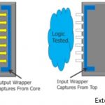
    At Cadence® DAC Technology Sessions, you’ll get in-depth presentations and demonstrations of our technologies and methodologies for developing the highest quality silicon, systems-on-chip, and complete systems at lower costs. Session options include our latest solutions in the areas of signoff, mixed signal, low power, RTL-to-GDSII, custom, functional verification, verification IP, system development and hardware-software integration, high-level synthesis, and IC packaging.

    REGISTER HERE

    [TABLE] border=”1″ cellpadding=”5″ style=”margin-top: 5px; border-collapse: collapse”
    |-
    | valign=”top” style=”width: 80px” | June 2, 2014
    | align=”center” valign=”top” style=”font-weight: bold; background-color: #dedede” | Suite 1
    | align=”center” valign=”top” style=”font-weight: bold; background-color: #dedede” | Suite 2
    |-
    | style=”font-weight: bold; background-color: #dedede” | 10:00 AM
    | valign=”top” style=”width: 300pxpx” | Benefits of Mixed-Signal, Open Access, Interoperable Flow
    | valign=”top” style=”width: 300pxpx” | Using Virtuoso Space-Based Router for Pin-to-Trunk Routing
    |-
    | style=”font-weight: bold; background-color: #dedede” | 11:00 AM
    | valign=”top” style=”width: 300pxpx” | Fast and Accurate Signoff Extraction for Advanced Nodes
    | valign=”top” style=”width: 300pxpx” | Characterization for Advanced Nodes
    |-
    | style=”font-weight: bold; background-color: #dedede” | 12:00 PM
    | valign=”top” style=”width: 300pxpx” | Tackling the Most Difficult ECOs with ‘Congestion and Timing Smarts’
    | valign=”top” style=”width: 300pxpx” | Electrically Aware Design: Addressing the Productivity Gap in Analog Design
    |-
    | style=”font-weight: bold; background-color: #dedede” | 01:00 PM
    | valign=”top” style=”width: 300pxpx” | RTL Design in a Physical World: Synthesis and Test
    | valign=”top” width=”300px” | High-Level Synthesis Improves Time to Market, Quality of Results, and IP Reuse
    |-
    | style=”font-weight: bold; background-color: #dedede” | 02:00 PM
    | valign=”top” width=”300px” | DDR4 Signoff: Chip-Package-Board IO-SSO Analysis
    | valign=”top” width=”300px” | Full Custom and Analog Advanced Node Design
    |-
    | style=”font-weight: bold; background-color: #dedede” | 03:00 PM
    | valign=”top” width=”300px” | Scalable Timing and Power Signoff Analysis with Tempus and Voltus Solutions
    | valign=”top” width=”300px” | Incisive Verification Apps: Automated Formal Solutions for Common Verification Issues
    |-
    | style=”font-weight: bold; background-color: #dedede” | 04:00 PM
    | valign=”top” width=”300px” | Advanced Mixed-Signal Verification Methodologies for ICs and SoCs
    | valign=”top” width=”300px” | SimVision and Incisive Debug Analyzer Reduce Debug Time from Days to Minutes
    |-
    | style=”font-weight: bold; background-color: #dedede” | 05:00 PM
    | valign=”top” width=”300px” |
    | valign=”top” width=”300px” | Accelerating Embedded Software Development with Cadence Rapid Prototyping Platform
    |-

    [TABLE] style=”width: 100%”
    |-
    | style=”width: 100%” | [TABLE] border=”1″ cellpadding=”5″ style=”margin-top: 5px; border-collapse: collapse”
    |-
    | valign=”top” style=”width: 80px” | June 3, 2014
    | align=”center” valign=”top” style=”font-weight: bold; background-color: #dedede” | Suite 1
    | align=”center” valign=”top” style=”font-weight: bold; background-color: #dedede” | Suite 2
    |-
    | style=”font-weight: bold; background-color: #dedede” | 10:00 AM
    | valign=”top” style=”width: 300pxpx” | System Interconnect Planning to Optimize Cross-Fabric Integration for Cost and Performance
    | valign=”top” style=”width: 300pxpx” | Full Custom and Analog Advanced Node Design
    |-
    | style=”font-weight: bold; background-color: #dedede” | 11:00 AM
    | valign=”top” style=”width: 300pxpx” | Scalable Timing and Power Signoff Analysis with Tempus and Voltus Solutions
    | valign=”top” style=”width: 300pxpx” | Incisive Verification Apps: Automated Formal Solutions for Common Verification Issues
    |-
    | style=”font-weight: bold; background-color: #dedede” | 12:00 PM
    | valign=”top” style=”width: 300pxpx” | High-Performance, Advanced-Node Encounter Digital Implementation
    | valign=”top” style=”width: 300pxpx” | SimVision and Incisive Debug Analyzer Reduce Debug Time from Days to Minutes
    |-
    | style=”font-weight: bold; background-color: #dedede” | 01:00 PM
    | valign=”top” style=”width: 300pxpx” | Foundry Qualified, Comprehensive Physical Signoff (Physical Verification and DFM) and Optimization f
    | valign=”top” width=”300px” | ARM v7 and v8 Based Accelerated System Development
    |-
    | style=”font-weight: bold; background-color: #dedede” | 02:00 PM
    | valign=”top” width=”300px” | DDR4 Signoff: Chip-Package-Board IO-SSO Analysis
    | valign=”top” width=”300px” | Spectre Simulation Technology – Addressing the Challenges of Advanced Node Design
    |-
    | style=”font-weight: bold; background-color: #dedede” | 03:00 PM
    | valign=”top” width=”300px” | Benefits of Mixed-Signal, Open Access, Interoperable Flow
    | valign=”top” width=”300px” | Electrically Aware Design: Addressing the Productivity Gap in Analog Design
    |-
    | style=”font-weight: bold; background-color: #dedede” | 04:00 PM
    | valign=”top” width=”300px” | Comprehensive Low-Power Solution – A Must for Today’s Complex Power-Managed Designs
    | valign=”top” width=”300px” | Metric-Driven Verification from IP to SoC with Incisive vManager Solution
    |-
    | style=”font-weight: bold; background-color: #dedede” | 05:00 PM
    | valign=”top” width=”300px” | RTL Design in a Physical World: Synthesis and Test
    | valign=”top” width=”300px” | What’s New with the Palladium XP Series
    |-

    |-

    [TABLE] border=”1″ cellpadding=”5″ style=”margin-top: 5px; border-collapse: collapse”
    |-
    | valign=”top” style=”width: 80px” | June 4, 2014
    | align=”center” valign=”top” style=”font-weight: bold; background-color: #dedede” | Suite 1
    | align=”center” valign=”top” style=”font-weight: bold; background-color: #dedede” | Suite 2
    |-
    | style=”font-weight: bold; background-color: #dedede” | 10:00 AM
    | valign=”top” style=”width: 300pxpx” | Comprehensive Low-Power Solution – A Must for Today’s Complex Power-Managed Designs
    | valign=”top” style=”width: 300pxpx” | Metric-Driven Verification from IP to SoC with Incisive vManager Solution
    |-
    | style=”font-weight: bold; background-color: #dedede” | 11:00 AM
    | valign=”top” style=”width: 300pxpx” | Tackling the Most Difficult ECOs with ‘Congestion and Timing Smarts’
    | valign=”top” style=”width: 300pxpx” | ARM v7 and v8 Based Accelerated System Development
    |-
    | style=”font-weight: bold; background-color: #dedede” | 12:00 PM
    | valign=”top” style=”width: 300pxpx” | Advanced Mixed-Signal Verification Methodologies for ICs and SoCs
    | valign=”top” style=”width: 300pxpx” | Using Virtuoso Space-Based Router for Pin-to-Trunk Routing
    |-
    | style=”font-weight: bold; background-color: #dedede” | 01:00 PM
    | valign=”top” style=”width: 300pxpx” | Scalable Timing and Power Signoff Analysis with Tempus and Voltus Solutions
    | valign=”top” width=”300px” | What’s New with the Palladium XP Series
    |-
    | style=”font-weight: bold; background-color: #dedede” | 02:00 PM
    | valign=”top” width=”300px” | High-Performance, Advanced-Node Encounter Digital Implementation
    | valign=”top” width=”300px” | Characterization for Advanced Nodes
    |-
    | style=”font-weight: bold; background-color: #dedede” | 03:00 PM
    | valign=”top” width=”300px” | System Interconnect Planning to Optimize Cross-Fabric Integration for Cost and Performance
    | valign=”top” width=”300px” | High-Level Synthesis Improves Time to Market, Quality of Results, and IP Reuse
    |-
    | style=”font-weight: bold; background-color: #dedede” | 04:00 PM
    | valign=”top” width=”300px” | Foundry Qualified, Comprehensive Physical Signoff (Physical Verification and DFM) and Optimization f
    | valign=”top” width=”300px” | Accelerating Embedded Software Development with Cadence Rapid Prototyping Platform
    |-
    | style=”font-weight: bold; background-color: #dedede” | 05:00 PM
    | valign=”top” width=”300px” |
    | valign=”top” width=”300px” | Spectre Simulation Technology – Addressing the Challenges of Advanced Node Design
    |-

    And the best for last:

    Mix, Mingle, and Enjoy!

    Ready to party? Mix, mingle, and have a fun time with your peers at the popular Denali Party by Cadence.

    For your musical entertainment, Disco Inferno will be back to rock the house. And this year, we’ll kick off the night with “Rockstar Karaoke” — your chance to sing with a live band and be the rock star you’ve always wanted to be! Sign up and select your song for Rockstar Karaoke via your registration form. We’ll let you know by email if you’ve been selected to participate.

    Didn’t make the Rockstar Karaoke cut? Don’t worry, you can still sing your heart out at the karaoke room at Slide, next door to Ruby Skye.

    We look forward to hanging out with you at the Denali Party!

    NOTE: You must pick up your wristband at the Cadence booth (#2610) before noon on Tuesday, June 3 or your reservation will be given to another guest.

    REGISTER HERE

    lang: en_US


    Taming The Challenges of SoC Testability

    Taming The Challenges of SoC Testability
    by Pawan Fangaria on 05-12-2014 at 10:00 pm

    With the advent of large SoCs in semiconductor design space, verification of SoCs has become extremely challenging; no single approach works. And when the size of an SoC can grow to billions of gates, the traditional methods of testability of chips may no longer remain viable considering the needs of large ATPG, memory footprint, and chip pins requirement for DFT and so on. Alternate methods need to be discovered. It pleasantly reminds me that the strategy of ‘Divide and Conquer’ to solve a problem with largeness works well here too. However, it’s easier said than done, in this case one needs to formulate the complete methodology of dividing the design for testability and then also re-combining it to complete the test at the full-chip level. How do we do that?

    It’s heartening to see a novel approach developed by Mentor Graphicswhere they use a hierarchical DFT methodology for testing the hierarchical cores and their interconnections separately, step-by-step, leading to full-chip testing.

    A core is the lowest hierarchical level at which test patterns are applied. It has a wrapper chain that can be configured to test the logic inside the core or the interconnect and glue logic external to the core. The core inside logic is tested in ‘Internal Mode’ when the ‘Input Wrapper’ is configured to launch values into the core and the ‘Output Wrapper’ is configured to capture responses. In the ‘External Mode’, the wrapper chain is reconfigured to launch values from the outputs to test chip-level glue logic and interconnect and capture responses at the inputs. In order to complete the DFT requirements, scan chains, compression logic, and test control logic are also inserted. With that it’s possible to generate a set of scan patterns at the core level that can subsequently be retargeted to the chip level. The end result of this step is a set of retarget-able patterns and a fault list containing all the coverage information for that pattern set. Clearly, the pattern generation time and the memory footprint for complete chip-level testing are significantly reduced by using this approach. Moreover, the procedures for different cores can be parallelised.

    During the ‘External Mode’ testing, all of the logic already tested for a core in ‘Internal Mode’ is removed from its netlist (except what is needed for external mode testing) to create what is called ‘graybox netlist’, thus making it possible to test the entire SoC without loading the full-chip netlist. In this process, a netlist reduction and hence memory footprint reduction of 10x or more can be easily possible, although it’s design dependent.

    For full-chip testing, retargeting of scan patterns at the full-chip level depends on how the cores are configured to be tested in ‘Internal Mode’ in the overall architecture of the chip. A mapping of ‘Internal Mode’ scan patterns from the core pins up to the chip-level pins has to be done. The pattern sets of multiple cores must be merged such that they can be simultaneously applied at the full-chip level.

    Above example shows how ‘Internal Mode 1’ groups cores 1 and 2 together whose patterns are retargeted and merged together. Similarly in ‘Internal Mode 2’ cores 3 and 4 are grouped together for retargeting and merging their patterns.

    After testing all cores, the interconnect and glue logic between cores is tested in external mode. The chip-level netlist is minimal in content with graybox netlist for each core. The external mode configuration accesses all the wrapper chains of the cores as well as any chip-level scan chains and runs the ATPG. After completing this testing, the final test coverage of the entire chip is computed by merging the fault lists saved from each core’s ‘Internal Mode’ pattern set into the ‘External Mode’ fault list.

    The DFT tool automation in Mentor’s Tessent tool suite supports this hierarchical methodology where all procedures as described above are automatically done. In fact, dedicated wrapper cells are not added all the time in order to conserve area and time. Instead, Tessent Scan automatically identifies and stiches shared wrapper cells (i.e. existing functional registers that can also serve to isolate primary inputs/outputs for test purposes) where possible.

    Above is a typical circuit example of a complete wrapped core with complete core netlist and its graybox representation. In the graybox, only wrapper chains and any combinational logic between the wrapper chains and the primary inputs/outputs of the core are required. This can reduce the netlist in the range of 10x to 20x. Tessent TestKompress automatically generates the graybox netlist.

    Tessent TestKompress includes all the pattern retargeting functionalities as described above along with the clock control logic and other requirements. Rick Fisette has described all these procedures in great detail in the whitepaperposted at Mentor website.

    With some up-front design planning, this methodology provides an excellent solution for the challenging task of testing large SoCs. The additional design effort required in this methodology is compensated richly in terms of at least 5x reduction in ATPG runtime, significant reduction in memory footprint (can be 10x or more depending on design), significantly reduced cumulative time, reduced pressure on tapeout as any ECO may affect a particular core and hence initiate retesting of that core only, and reduced dependence on top-of-the-line machine for testing. It’s simply a great methodology!

    More Articles by Pawan Fangaria…..

    lang: en_US


    A Brief History of the Apple MacBook Pro

    A Brief History of the Apple MacBook Pro
    by Daniel Payne on 05-12-2014 at 5:49 pm

    I’m typing this blog today with my trusty Apple MacBook Pro – a 17″ laptop with matte display and 16GB of RAM, but don’t stereotype me as an Apple fanboy because I also own the fantastic Samsung Galaxy Note II phone (aka phablet). Some industry pundits would have us believe that desktops and laptops are going extinct like the Dodo bird, while tablets and mobile phones are ramping up volumes. The MacBook Pro line of laptops from Apple came onto the scene in 2006 and are instantly recognized by the iconic white Apple logo, thin profile, and use of aluminum construction. For many tasks you simply need a real keyboard and mouse to get the job done, along with portability for convenience.


    13″, 15″ and 17″ MacBook Pro laptops

    The MacBook Pro laptops are priced at a premium, about 2X the price of any PC-based laptop. What you get for that premium is:

    • An aluminum laptop construction that doesn’t flex and twist like plastic
    • Ultra-thin profile (what PC makers now call Ultrabook)
    • High-end audio speakers, built-in
    • Choice of glossy or anti-glare displays (my favorite)
    • Battery life to last four to eight hours, depending on work load and screen size
    • The intuitive Mac OS X operating system (largely cloned by Microsoft Windows)
    • Quiet operation with minimal fan noise
    • BSD Unix for the geeks that need to use a command line

    Generations

    There have been three generations of MacBook Pro laptops, all using CPU chips provided by Intel. The big question for the future is, “Will Apple stick with Intel CPU chips, or switch to it’s own A-series CPUs also used in the iPad and iPhone products?”

    First generation MacBook Pros came with: 15″ and 17″ displays, webcam, optical drive, ExpressCard/34 slot, USB 2.0 ports, FireWire 400 port, Gigabit Ethernet port, Bluetooth 2.0 and 802.11 a/b/g for WiFi. Updates added FireWire 800 port, increased RAM, and Intel cores with 45nm processing in 2008. At that same time Apple launched the MacBook Air laptops which replaced the hard drive with SSD, thinner profile and lighter weight, removing the optical drive. ATI and Nvidia provided the graphics processing from 2006 to 2008, often alternating vendors each release.


    MacBook Air, 11″ and 13″ Displays

    Late in 2008 the 2nd generation of MacBook Pros were launched, and the aluminum body was called “unibody” construction, instead of multiple pieces screwed together. By 2009 you could get three display sizes: 13″, 15″ and 17″. The battery became non-removable, a trend against any user-replaced parts which unfortunately continues today. In 2010 the CPU was an Intel Core i5 or Core i7. A new high-speed connector called Thunderbolt came out in 2011, and so far mostly Apple and Intel are promoting this. Sadly in 2011 Apple also discontinued the 17″ model, instead offering only two display sizes 13″ and 15″. Graphics vendors switched again to Nvidia, then Intel.

    2012 was the year Apple decided to promote higher pixels per square inch, also called Retina Display with a 15″ display holding 2,880 x 1,800 pixels, starting the 3rd generation. The optical drive is now removed, so you have to buy an external unit for any spinning media like CD or DVD. Oddly enough the Ethernet and FireWire 800 ports were also removed, requiring you to buy more adapters to get these features back. RAM is soldered to the motherboard, so choose your model wisely because there is no field-upgrading any more. SSD drives became available for higher performance. Intel swept the graphic processors in this generation. The Intel CPU is the Core i7 with four cores, 8 threads, clocked at 2.6 GHz.


    Intel Core i7. Source: Legit Reviews

    Summary

    Apple does think different when it comes to laptops, because they offer two models in the MacBook Prowith 13″ and 15″ displays, and two models in the MacBook Air with 11″ and 13″ displays. If portability is your number one factor, then consider the MacBook Air. If biggest display and performance are deciding factors, then go for the MacBook Pro series.

    I’m personally waiting for Apple to bring back the MacBook Pro in a 17″ size with Retina Display. Until then, I’m happy to use my 3 year-old MacBook Pro daily. One legacy app that I run on Windows 8 is Quicken, so I use the Parallelsvirtualization software on my MacBook Pro. I’ve even run Redhat Linuxon my laptop using Parallels. If you agree that Apple should bring back the 17″ MacBook Pro, then join my Facebook page to show your support.

    Further Reading

    lang: en_US


    A Brief History of MunEDA

    A Brief History of MunEDA
    by Daniel Nenni on 05-12-2014 at 4:56 pm

    In 2002, MunEDA was launched under the guidance of EDA academic veterans and IEEE fellows Prof. Kurt Antreich and Prof. Helmut Gräb (TUM Munich Technical University ) which represented 20 plus years of EDA research and experience. All MunEDA tools are combined in a tool suite called WiCkeD[SUP]TM[/SUP]. The tool suite brand was derived from the powerful WCD Worst Case Distance algorithm that is used in MunEDA tools for circuit design analysis and optimization.

    In 2002, the portfolio of MunEDA tools limited to some methods for circuit analysis and optimization of smaller blocks such as OpAmps, Bandgaps or similar analog circuits. The most advanced process technologies of at that time was 90nm with 65nm coming up on deck. Monte-Carlo as yield analysis method was in its infancy and rarely utilized. Driven by global customers such as Infineon, Samsung, STMicroelectronics, Altera, SKHynix and others MunEDA would enhance and apply its outstanding algorithms into leading-edge circuit design areas such as wireless, IP and memory design.

    In 2005, MunEDA published its new RSM (Response Surface Model) Circuit Modeling tools that can be used to model larger blocks to combine transistor-level and system-level simulation and speed up the design verification time and effort. This method has been adopted by customers such as ST for PLL design acceleration.


    In 2006, MunEDA started to have annual MUGM MunEDA User Group Meetings where MunEDA customers and partners present their MunEDA related experiences with design and tape-out cases. In addition, MunEDA also has hosted annual global MTF (MunEDA Technical Forums) and has reached nearly 1000 attendees.

    More than 200 technical papers have been published at MunEDA conferences since the 2006 inception of MUGM.

    In 2008, MunEDA enhanced their tool flow with MTB Multi-Testbench-Capabilities that enables to use WiCkeD for larger and multi-project designs.

    In 2010, MunEDA published the new schematic migration tool SPT for automated design porting and migration of existing IP between different foundry process technologies. This tool has been developed in collaboration of MunEDA’s foundry partner TSMC and is since in use with numerous MunEDA customers and partners worldwide.

    In 2012 MunEDA enhanced all MunEDA tools and solutions to be used with discrete circuit analysis and optimization for latest FinFET, FDSOI and BiCMOS process technology. In the same year MunEDA received the EDA Achievement Award 2012 from edacentrum.


    In 2013, the WiCkeD tool suite was joined by a new enhancement of reliability and aging effects. It the MunEDA’s corporate edict to continuously meet the challenges of design and automation required by our existing customers and the new customers we look forward to meeting and serving.

    Of course MunEDA will be at DAC. They will be in booth 2213. MunEDA’s website is here.

    Webinar on Full-Custom Low Power Design Methodology


    Teach Yourself Silvaco

    Teach Yourself Silvaco
    by admin on 05-12-2014 at 10:53 am

    In the dim and distant past, if you wanted to learn how to use a particular EDA tool then you would go on a training course. This would often be multiple days and often a significant dollar investment too. For most EDA companies, that option still exists and the big 3 have quite extensive training catalogs.

    But nowadays it is often easier to learn from online material that can be consumed in smaller bites, focused on specifically the area that you are most interested in. Silvaco has hundreds of examples on their website. The industry grade examples are carefully designed to reflect the key product capabilities and functionality, and have been derived over many years from real benchmark experience and publications. The examples can be used by beginners and advanced users for product evaluation, teaching purposes, and self-training.

    The typical example provides all the input files that you require to run the Silvaco tool for some particular application.

    Here is one on table lookup for SmartSpice.Requires: SmartSpice & Smartview
    Minimum Versions: SmartSpice 4.6.5.R

    An E element voltage source (VCVS) can be used with a Look-up table of values to change the output level. In this example the input is swept between 2 and 8 volts while the output level changes at 3, 4 and 5 volts goverened by the transfer characteristic of the Look-Up table.

    The input deck is a SPICE file containing the setup of the bias circuit for the sense inputs of the E(VCVS) element, and the Look-up table to vary the corresponding output voltage levels.

    To run the simulation, Source the input deck and press the green run button. When the simulation completes, the tabular results are shown in SmartSpice GUI window.

    Plotting the output waveforms in a smartview window you can see the ramped voltage (vdd), input of the E element v(vcvs) and the corresponding output voltage v(tso) due to the Look-up table values.

    You can plot v(tso) vs v(vcvs) waveform to directly check the Look-up table by setting v(vcvs) as the scale parameter (a Smartview feature).

    This example is an introductory one but there are also much more advanced examples showing more sophisticated aspects of the Silvaco toolsets.

    Silvaco’s worked examples area all here.