llmda newsletter ad (2)

Synopsys Revamps Formal at #51DAC

Synopsys Revamps Formal at #51DAC
by Paul McLellan on 06-30-2014 at 6:02 pm

Synopsys announced verification compiler a couple of months ago and dropped hints about their static and formal verification. They haven’t announced anything much for a couple of years and it turns out that the reason was that they decided that the technology that they had, some internally developed and some acquired, wasn’t a good basis for going forward and they needed to rebuild everything from the ground up. Compared to when their technology was developed, there was advanced power management, hundreds instead of a few clocks, complex protocols and complex interconnect. At DAC earlier this month they announced their new products.

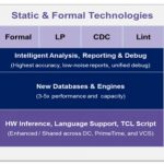
They use the front end of VCS so that anything that can be loaded into VCS can be loaded into their static and formal tools. That is not to say that their formal tools, in particular, can prove a whole SoC correct, that is just unlikely to ever happen. But they can check, for example, all the connectivity or the clock-domain-crossing (CDC) signals on a whole chip, taking all the reconvergence into account.

The performance is way up on prior performance. 4X improvement in low power checks, 60X up on formal checks and 180X on sequential checks. That’s a lot.

On low power static checking they have UPF checks, architectural checks, functional and structural checks and power-ground checks. They support all the latest low power design techniques and have a very close alignment with the implementation flows. One of the big issues with static checking is that one error can cascade lots more and so there is a high noise-to-signal ratio. A hundred errors lead to 20,000 violations and it is hard to find the real errors that need to be fixed.


The CDC checking works at the full-chip level so can find deep reconvergence bugs. It uses the same setup scripts as DC which makes adoption straightforward. It recognizes all sorts of synchronizer implementations on clock boundaries: extra FF, FIFOs, mux, handshakes and more.

On the formal side they have rebuilt formal engines from scratch for the toughest challenges. Formal is a weird technology, if one approach can prove something then it doesn’t matter that others cannot. So different engines under the hood can make the whole tool more powerful. And smart users know that if one formal tool can prove something it doesn’t matter that another cannot and so they often use several tools in parallel. The formal tools produce a waveform when they find an issue (a waveform that causes the assertion to fail) and this is fully integrated with the Verdi debug that Synopsys acquired with SpringSoft, making tracking down and fixing the root-cause a lot easier.


So new technology, several times faster, much higher capacity and easier to use. And all tied into the standard interface of verification compiler.


More articles by Paul McLellan…


Virtual Prototype Update from #51DAC

Virtual Prototype Update from #51DAC
by Daniel Payne on 06-30-2014 at 12:07 pm

EDA industry pundit Gary Smithhas been talking about the electronics industry adopting an ESL tool flow for decades, so it was my pleasure to speak with Bill Neifertof Carbon Design Systemsat DAC this month because his company has been offering both tools and models that enable a virtual prototyping design flow.

Continue reading “Virtual Prototype Update from #51DAC”


The Intel Resurgence?

The Intel Resurgence?
by Daniel Nenni on 06-30-2014 at 8:00 am

There is an interesting article on Seeking Alpha about Intel. Interesting because it is written by someone with both fabless semiconductor experience and a talent for strategic thinking. It’s a good read and like most Seeking Aplha semiconductor articles the comments are hilarious. Give the guy a penny and click over HERE, he deserves it:

Little understood by analysts or investors is the fact that Intel has always operated as a one-product company that spins out dozens of derivatives. Desktop, mobile and server chips originate from one common core. This leads to ramping of millions of units quickly and this is key: at incredibly high yields. Every time the company tries to implement a new core and split the markets, it fails. This occurs often and it is why Atom is not the future. Broadwell is well designed to continue the one core processor for all markets and selling from $30 to $6000 depending on number of cores, cache sizes, performance and power.

Full disclosure: I know the author (Ed McKernan), he started his writing career on SemiWiki and we happen to agree on most things semiconductor with the exception of Apple using Intel as a foundry. It’s not gonna happen Ed!

I too believe Intel will exit the Atom based SoC chip business. There is serious competition inside Intel between the microprocessor and mobile group and at some point in time there will no longer be room for both, my opinion. I’m told about 10,000 employees are involved with the Intel mobile effort so this would be a serious RIF. It would also be a serious piece of humble pie but I think Intel CEO BK is the right guy to eat it and be stronger as a result. Let’s see what Q2 2014 earnings bring for Intel mobile, my guess is it will be yet another billion dollar loss.

The funniest comment thus far is an attack on me of course:

Dan,
Let’s keep in mind what you consider to be an expert opinion.

Back in mid-2011 you predicted Intel’s 22nm FinFET was a billion dollar mistake, and you claimed TSMC’s 3D IC technology was already in production yet it hasn’t been seen in public for 3 years now, unless by production you mean the production of powerpoint slides.
http://bit.ly/TG5xN9.

About six months after SemiWiki went online I wrote an article about the difference between a 3D transistor (FinFET) and 3D IC (packaging). This guy still does not get it. At that time SemiWiki had about 15k users (viewers) and close to 20k people read the article so that was a big deal. Three years later we have more than a million users and articles about Intel and TSMC still draw the most attention which is why I write them. I also learn as I write, which is the real motivation behind blogging, industry knowledge. Unfortunately sometimes it’s painful to look back at what I’ve posted and this is one of those times.

This is what I wrote:

In May of this year Intel announced Tri-Gate (FinFET) 3D transistor technology at 22nm for the Ivy Bridge processor citing significant speed gains over traditional planar transistor technology. Intel also claims the Tri-Gate transistors are so impressively efficient at low voltages they will make the Atom processor much more competitive against ARM in the low power mobile internet market.

Okay, so far so good.

Time will tell but I think this could be another one of Intel’s billion dollar mistakes. A “significant” speed-up for Ivy Bridge I will give them, but a low power competitive Atom? I don’t think so.

The BayTrail 22nm SoC was in fact a billion dollar contra revenue failure but I have no idea what I was thinking when I wrote this:

Intel already owns the traditional PC market so trading the speed-up of 3D transistor technology for lower power planar transistors is a mistake.

Say what? :confused:

More Articles by Daniel Nenni…..

lang: en_US


What can you do when your fab closes down?

What can you do when your fab closes down?
by Daniel Nenni on 06-29-2014 at 4:00 pm

A recent report from IC Insights described 72 wafer fabs that have closed in the past five years. Eight more plants have gone in 2014, showing the trend is continuing.

This leaves their customers with a problem: what can they do when the fab shuts down? Some may recognise that their own technology has reached the end of its life and work on generating a replacement while others will place a ‘last time buy’ to stockpile as many chips as they can. However, most will be left with a headache as they go looking for a new supplier.

Moving any existing circuit from one foundry to another is difficult and it’s much worse when dealing with legacy chips. Detailed databases may be difficult to locate and the original design team is likely to be long gone, leaving little circuit knowledge for the product. Companies may be left with a few files and a pressing need to find a new supply of silicon.

As process migration specialists, IN2FAB often works with companies who have to find a new foundry. A redesign will be time consuming and too costly when no new functionality is required so a migration based path to a new supplier is very attractive.

When facing this problem, the chip’s owner should gather as many design files as possible and a GDSII file and a netlist is usually the minimum. A schematic database is preferred although the tools used to create them may be gone so translators can be used to pull them in to a Cadence system to match the new foundry’s PDK. A layout database made with parameterised cells is useful but polygon based layout will suffice.

Also read: IC Manufacturers Close or Repurpose 72 Wafer Fabs from 2009-2013

Analog and mixed signal circuits are typically defined by the transistors’ voltage thresholds and matching of the passives. If the ohms per square in the target process are much lower, resistors will have to grow which can lead to spacing problems and a similar match must be made for capacitors. IN2FAB usually conducts a detailed feasibility study to identify similarities and differences between components which is essential when choosing the new foundry and process.

Delay files for digital circuits may not be to hand which makes regeneration through place and route almost impossible. Instead, the design can be migrated as a custom circuit to exactly match the original and maintain the placement and routing as before. This retains balance and prevents the introduction of new timing offsets. Digital circuits can often move to a smaller node and gate sizes and routing adjusted to meet the new rules without losing the integrity of the original circuit.

Other elements like bond pads and ESD or difficult components like inductors must also be considered but the key to the migration is to match the design to the new process and use automation to modify the design as needed. While some dedicated engineering input may be needed to address fine details, the automation in our own EDA technology means that the chip can usually be transferred to the new process in weeks.

Losing a foundry is a problem but it needn’t be a disaster. Migration technology can move circuits to a new process from basic design files or old CAD systems and bring them up to date, giving them a new lease of life. Redesign is expensive and putting designers to work on old products is poor allocation of resources. Migration presents an effective alternative and is usually the fastest way to move circuits to a new foundry.

Tim Regan
President and CTO
IN2FAB Technology


lang: en_US


This is How We Get One Million Design Starts!

This is How We Get One Million Design Starts!
by Daniel Nenni on 06-28-2014 at 10:00 am

One of the most interesting demos at #51DAC was the eSilicon GDS II online quote system for TSMC. Probably because eSilicon was one of the most interesting companies exhibiting this year. While writing the book “Fabless: The Transformation of the Semiconductor Industry” we took a close look at the history of fabless semiconductor design. An instrumental part of that history was the ASIC business model where design teams big and small could toss a design spec and a big wad of cash over a wall and get a chip manufactured. eSilicon transformed the ASIC business model by creating a success based partnership with customers that has resulted in hundreds of designs that may have never been.

Also Read: We Need One MILLION Design Starts!

The next transformation you will see is what I call putting the “e” back in eSilicon by internet enabling semiconductor manufacturing. Paul McLellan wrote about it recently: Online MPW Quote Systemand GDS II Online for TSMC. The goal here is to enable design starts and get them into production as quickly and as error free as possible. This is the perfect vehicle for IoT designs, absolutely!

eSilicon’s online quote system for multi-project wafer (MPW) shuttle services delivers instant, executable quotes. The service is accessed through user-friendly web or smartphone interfaces allowing users to evaluate the wafer cost of multiple options in real time at no cost or obligation.

eSilicon’s GDSII portal offers the ability to fully specify the manufacturing process requirements for submission of a GDSII design to TSMC for manufacturing. The required manufacturing process information is specified through a series of easy-to-use menus, along with requirements for packaging, testing and delivery. An executable quotation from eSilicon is provided that includes non-recurring engineering (NRE) pricing and unit pricing for the system-on-chip (SoC) device.


Calling all IoT entrepenuers!

Next month SemiWiki and eSilicon will be doing a webinar on the GDS II portal. I hope to see you there:

GDSII online quoting webinar overview
Choosing all the options necessary to tape out a completed GDSII design for volume manufacturing can be a daunting task. Which process node, what process options, which package and what tester to use are just some of the important questions to answer. And there are many optional services to consider as well. It can take several weeks to months to collect all the information to create a single, complete quotation.

What if you could go to one place and browse all the options available, then generate a complete, executable quotation in minutes? Thanks to eSilicon and TSMC, it is now possible to do just that for a wide variety of TSMC technologies.

What you will see
In this informative, interactive webinar you will witness an actual quote being generated based on real designer input. You will be taken through all the steps required to generate a complete, executable quotation that addresses tapeout costs, optional services and volume production pricing for a new chip design. And we’ll do it all in about 10 minutes using the automated GDSII quoting tool.

We’ll also take you on a journey of discovery, highlighting how various options can be traded off and how those trade-offs impact the final quotation. If you plan to tape out a design for volume manufacturing, you must attend this webinar.

REGISTER HERE

More Articles by Daniel Nenni…..

eSilicon, a leading independent semiconductor design and manufacturing solutions provider, delivers custom ICs and custom IP to OEMs, independent device manufacturers (IDMs), fabless semiconductor companies (FSCs) and wafer foundries through a fast, flexible, lower-risk, automated path to volume production. eSilicon serves a wide variety of markets including communications, computing, consumer, industrial and medical. www.esilicon.com.

lang: en_US


High Level Synthesis update from #51DAC

High Level Synthesis update from #51DAC
by Daniel Payne on 06-27-2014 at 8:00 pm

Every since Synopsys dominated the logic synthesis market in the 1980’s we’ve had something called HLS – High Level Synthesis, meaning something higher than what Design Compiler can understand as input. At DACthis year I met with Mark Milligan of Calypto to get an update on what’s new with HLS. I first met Mark when he was at Sunrise Test Systems in the 1990’s and I was at Viewlogic, so I’ve kept in touch with him over the years.

Continue reading “High Level Synthesis update from #51DAC”


I’ll be with you in a second

I’ll be with you in a second
by Don Dingee on 06-27-2014 at 3:00 pm

One aspect of always-on is power conservation, being able to respond to events without having a device constantly in full-power mode. This month, the announcement of the Amazon Fire Phone and details revealed about the Google Android Wear SDK suggest another important dimension: the competitive advantage of rapid, frictionless engagement. Continue reading “I’ll be with you in a second”


Standard Cell, IO and Hard IP Validation update

Standard Cell, IO and Hard IP Validation update
by Daniel Payne on 06-27-2014 at 1:26 pm

Every SoC team uses libraries of cells to get their new product to market quicker: Standard Cells, IO Cells and Hard IP blocks. One immediate question that comes to my mind is, “How clean are these cells?” Validating your cell libraries first makes sense, and will ensure that there are fewer surprises as your chip gets closer to tape-out time. At DAC this year I stopped by the booth of Fractal Technologiesand had a conversation with founders Rene Donkers and Johan Peeters to get an update on their EDA business.


Continue reading “Standard Cell, IO and Hard IP Validation update”


Electronics growth positive around the world

Electronics growth positive around the world
by Bill Jewell on 06-26-2014 at 6:00 pm

Electronics production growth has turned positive in 2014 for all key geographic regions. The graph below shows three-month-average change versus a year ago for electronics production in local currency through April 2014. Total industrial production is used for Europe (EU countries) and South Korea since electronic production data is not available. The data is from government sources.


China continues to show strong growth in electronics of 10% or higher. Taiwan electronics was in a significant decline throughout 2012 and 2013 but returned to growth of 5% in April 2014. Japan electronics experienced a major decline following the March 2011 earthquake and tsunami. Japan’s electronics growth has been positive since November 2013, ranging from 4% to 8%. U.S. electronics went from positive growth in 2012 to declines of 1% to 7% in each month of 2013. The U.S. turned positive in January 2014, showing growth in the range of 2% to 4% through April. Europe’s industrial production followed the same general trend as U.S. electronics, turning positive in October 2013 and growing about 3% in each month of 2013. South Korea’s industrial production oscillated between positive and negative in 2013, but has been positive since December 2013.

Two key drivers of electronics and semiconductor growth over the last few years have been smartphones and tablets. The growth rate of these products has been slowing over the last several quarters. Tablets have slowed from over 100% year-to-year growth in 2012 to only 4% in 1Q 2014, according to IDC. Smartphone growth has decelerated from close to 50% in 2012 and the first half of 2013 to 24% in 4Q 2013 and 29% in 1Q 2012.


Despite the slower growth in the last few quarter, both tablets and smartphones are expected to show healthy growth for the year 2014. Gartner expects tablet growth of 39% and NPD DisplaySearch projects 26%. IDC lowered its forecast in May to 12% from its March forecast of 19%. IDC expects large display smartphones to take away some of the potential market from tablets. Smartphones are forecast to grow between 24% and 34% in 2014 according to Gartner. IDC is projecting 19%.

[TABLE] border=”1″ style=”width: 600px”
|-
| style=”width: 422px” | 2014 Unit Growth Forecasts
|-
| style=”width: 108px” | Tablets
| style=”width: 98px; text-align: center” | 39%
| style=”width: 216px” | Gartner, March
|-
| style=”width: 108px” |
| style=”width: 98px; text-align: center” | 26%
| style=”width: 216px” | NPD DisplaySearch, Feb.
|-
| style=”width: 108px” |
| style=”width: 98px; text-align: center” | 12%
| style=”width: 216px” | IDC, May
|-
| style=”width: 108px” |
| style=”width: 98px” |
| style=”width: 216px” |
|-
| style=”width: 108px” | Smartphones
| style=”width: 98px; text-align: center” | 24% to 34%
| style=”width: 216px” | Gartner, Feb.
|-
| style=”width: 108px” |
| style=”width: 98px; text-align: center” | 19%
| style=”width: 216px” | IDC, Feb.
|-

What is the next big driver of growth for electronics and semiconductors? One potential answer is the further evolution of computers and mobile phones into a single device to handle most of people’s computing and communication needs. It will probably several years of technological and design innovation before this type of device becomes mainstream.
In the near term several applications will help stimulate electronics and semiconductor growth:

  • Automotive production has grown steadily over the last four years. Safety, entertainment, navigation and communication applications are driving increasing electronics and semiconductor content in automobiles.
  • Television sales will see higher growth as more consumers purchase Ultra High Definition (UHD or 4K) TVs. However the high prices of UHD TVs will limit the market to early adopters for a few years.
  • Wearable devices for tracking fitness and health are becoming popular. The market for these devices is currently small but fast growing.
  • The “internet of things” (IoT) is getting a great deal of publicity. Basically it refers to connecting a wide range of devices to the internet to be remotely monitored and controlled by a PC, tablet or smart phone. Home security and energy management are two key IoT applications which are seeing acceptance in the market. However some of the proposed IoT applications seem to be a technology in search of a need.

The current outlook for electronics and semiconductors is good based on production statistics. Traditional and emerging devices should be able to sustain growth for at least the next few years. Our May forecast at Semiconductor Intelligence was for semiconductor market growth of 10% in 2014 and 9% in 2015. This forecast certainly looks achievable based on recent trends.

lang: en_US


IP Management Update at DAC

IP Management Update at DAC
by Daniel Payne on 06-26-2014 at 12:42 pm

To keep track of my business and personal finances I use software from Quicken, but for an SoC with hundreds of IP blocks how do you keep track of everything? The answer is found in the growing field of EDA tools for IP management, and at DACearlier this month I sat down with Neil Handof Methodics to get an update on what the industry trends are.