There has been a lot of railing lately about how we don’t have quite the right chips for the upcoming wave of wearables. Chips one would drop in a smartphone are often overkill and overpowered, burning through electrons too quickly. Chips one would use for a simple control task generally lack peripherals and performance, offsetting their low power advantage. Continue reading “What’s not quite MCU, and not quite SoC?”

Can Intel be a Leading Semiconductor Foundry?
This is the third part of a series answering the most frequently asked questions I get from Wall Street. Please read the previous two articles on Intel’s Manufacturing Lead and Intel’s SoC Challenge before flaming me in the comment section. First let’s look at why there is a foundry business and go from there.
The big semiconductor companies are the ones who started the foundry business in the 1980’s by renting out excess capacity to help pay for manufacturing costs. Unfortunately for them this unleashed a new era of semiconductor innovation and hundreds of fabless companies to compete with.
It all began when Dr. Morris Chang worked on a project for TI where manufacturing was done by IBM. This was one of the early semiconductor foundry relationships. Morris also noticed that top TI engineers were leaving and forming their own semiconductor companies. Unfortunately the capital requirement of semiconductor manufacturing was a gating factor. The cost back then was $5-10M to start a semiconductor company without manufacturing and $50-100M to start one with manufacturing.
The first two fabless companies, Chips and Technologies (C&T) and Xilinx, are profiled in the book “Fabless: The Transformation of the Semiconductor Industry” but here is the short version:
In the case of Xilinx, employees of a semiconductor company made a proposal internally for a programmable device. That proposal was rejected so the employees resigned and Xilinx was founded. Originally Xilinx’s business plan included building a fab to attract funding but in reality they were committed to the fabless model. C&T took the same approach with the “build a fab head fake” while negotiating fab space with Japanese semiconductor companies. Today Xilinx is the FPGA leader and it wasn’t long before C&T had more chips on a PC motherboard than Intel which lead to Intel acquiring them for $400M in 1997. All thanks to the fabless business model.
Unfortunately the “rent extra fab space from semiconductor companies” business model had one serious flaw. You were at the mercy of a company who did not really have your best interests at heart. Sometimes they competed with you, other times your business was not on the top of their priority list, and your IP was always at risk.
Today the Pure-play semiconductor foundry business model put in place by TSMC and replicated by UMC, SMIC, GlobalFoundries, and others is the backbone of the fabless semiconductor ecosystem. The ability to second, third, and even fourth source your design is a big part of that backbone. Unfortunately the fumbling of 28nm by everyone except TSMC has opened the door again to the big semiconductor companies who have excess fab space. For Intel this seems to be a tar pit if 14nm is any indication (Intel has no big volume customers at 14nm).
Of course I said the same thing about Samsung when they started in the foundry business 5+ years ago. Recent events however have changed my mind. Their ability to work with the fabless ecosystem and build relationships with other manufacturers (GlobalFoundries and STMicroelectronics) speaks volumes. Their aggressive pricing will also enable more design starts and overall industry growth. Samsung will be a major force in the foundry business starting at 14nm, absolutely.
Given that, the question you really have to ask yourself is: Can Intel survive a foundry turf war between TSMC and Samsung?
More Articles by Daniel Nenni…..
lang: en_US
Jasper at DAC
Wait, didn’t Cadence just acquire Jasper. Why is there a Jasper at DAC post?
So the big event is lunch on Tuesday, on Treasure Island. For out of towners that is the island in the middle of the bay bridge (actually just half of it). Food trucks, awesome views of the bay, and really cool street performers. There will be street magic, a live band, a juggler, and a very unique bubble blower that will blow bubbles with people inside them! Full details and registration here.
Of course there is stuff going on in the booth too. Booth 2033. Two seminars, presented several times a day.
Low power: 3 Ways Jasper Can Reduce Your SoC’s Power Consumption Now
Low power optimization techniques significantly impact the structural and behavioral elements of your original design. Such changes can be very difficult to verify in simulation, whereas formal analysis enables exhaustive verification. In this seminar we will show three methodologies that leverage Jasper’s Formal Apps to automatically generate assertions and data that verify that the power description matches UPF/CPF power intent & guidelines, and verify that the power intent does not create any new hazards. Specifically, clock gating, retention optimization & partial retention verification, and the fundamental enabling of more power domains & increased complexity will be shown in context of case studies where these flows have saved substantial schedule time and power budget on real world projects.
5 Ways Formal Can Offload (and even replace) Simulation Today
Since formal analysis was productized over a decade ago, engineers, CAD managers, and EDA vendors have often speculated how and when this technology would proliferate. This isn’t just an academic question given the very compelling fact that formal analysis provides exhaustive results for any problem it’s applied to. Wouldn’t it be great if the many uncertainties around the completeness of verification could eventually be eliminated with this powerful technology? In this seminar we will show how formal is the “right tool for the job” in five popular use cases that were once the exclusive province of simulation. For example, in some cases – like SoC Connectivity checking — formal can displace simulation completely. However, in flows like X-Propagation verification, simulation and formal can be used side-by-side to achieve the necessary confidence level. References to real world customer reports will be included.
Also, Broadcom and NVidia are presenting as part of the designer track.
Formal and static methods, which analyze a design directly rather than depending on large numbers of simulation vectors, are becoming increasingly important in the world of modern design. In the first part of this session, real-world practitioners who have been successful with formal verification describe case studies and use them to supply useful advice for those who wish to achieve similar results. Then we move on to describe some new and powerful uses for static and formal techniques in conjunction with other tools and methods, providing new insights into IP integration, clock domain crossings, power issues, and clock/reset design.
But wait, there’s more. A couple of Design Insight Tutorials.
DAC INSIGHT: Using Formal to Achieve Coverage Closure
Whether using simulation or formal methods, achieving verification closure requires the design team to answer the following questions with a high degree of confidence:
1. Does the verification environment sufficiently analyze the design to confirm the DUT meets the product specification?
2. Which parts of the design and use cases have been fully verified, and which need more attention?
Answers to these questions require analysis not only of stimuli coverage, but also of observation coverage, that is, the extent to which responses to stimuli are actually observed by the verification environment.
The exhaustive nature of formal methods encompasses both stimuli and observation analysis and coverage. In contrast, dynamic methods apply stimuli and measure only stimuli coverage. Dynamic methods cannot measure observation coverage, making verification closure tedious, time-consuming and uncertain.
This session will cover various coverage metrics for formal verification and provide a recommended methodology towards how formal verification technology and the associated metrics can be leveraged to accelerate the overall coverage closure process; and in the process reduce – and in some cases make redundant – corresponding dynamic simulation efforts.
DAC INSIGHT: Formally Addressing Hardware Security
Complex SoC’s, such as those for cell phones, game consoles, medical devices, vehicles, and servers contain secure information that’s valuable for unauthorized parties to exploit. Unfortunately, manual inspection by experts doesn’t scale, and simulation-based or emulation approaches rely on the inconsistent hacking abilities of verification engineers. Inevitably many corner cases are left unchecked, leaving open pathways for attackers. This session will focus on formal methods to tackle security verification challenges and make hardware impervious to attackers. Specifically, it will demonstrate how formal verification can be used exhaustively prove that attackers cannot breach the hardware authentication logic and registers, and/or read or alter the secure data through illegal logic paths. All of the above will be demonstrated in the context of several real-world case studies.
Details on the Jasper website here.
Automotive Focus @ #51DAC!

For the first time in DAC history there is an automotive track. Being a car person myself this is exciting news. I had a quick chat with Anne Cirkel, Vice Chair of DAC, and she sent me the following information to get us prepared for our week in San Francisco. The weather is going to be great so plan accordingly!
Ever increasing feature content enabled by electronics and software and the associated complexity has made development of automotive electronics and software amongst the largest challenges for the automotive industry. Today, the functionality, efficiency, time-to-market, cost, quality, safety, and security of a new vehicle are determined more by embedded systems and software than by any other factor. The Automotive Track is a new, unique forum addressing design automation and design methodologies to enable automotive designers and integrators to meet their unprecedented challenges.
3 new major initiatives at DAC: Automotive, IP, SecurityAutomotive
The idea to look at automotive was born at the strategy committee meeting when Soha Hassoun was Vice Chair of DAC. When you think about it, automotive electronics design is a perfect field for design automation – and DAC is THE design automation conference. Just a few data points from Wally’s visionary talk at DAC last year in Austin:
The DAC EC learned over the last couple of years that if you have a new initiative and want it to work from a program perspective you need the right people on board to drive it. We invited two industry specialists onto the Executive Committee for DAC and we now have an exciting program with two tracks on Tuesday and Wednesday. The two people on the committee are Samarjit Chakraborty from TU Munich and Tony Cooprider from Ford.
Tuesday Keynote:
Delivering smart Automobiles through Electronics and Software – Dual Keynote by Jim Tung from the Mathworks, and James Buczkowski from Ford Motor Company
SKY talks:
Managing Multi-Scale, Multi-Physics Challenges in the new generation of automotive systems by Walid Abu-Habda from ANSYS
Securing the Internet of Cars by Dave Kleidermacher from Green Hills Software
Pavilion Fireside Chat:
Automotive Engineers love Design Automation – Wally Rhines and James Buczkowski
Exhibit Floor:
Automotive Village with ANSYS, Dassault Systems, MathWorks, Mentor, Simuquest, Synopsys and Wrightspeed who will bring in their flatbed truck with their plug-and-play repower kit:
Wrightspeed is a powertrain company; we do not manufacture vehicles. We like to make things go, and we like doing it well. Built on a tradition of quality systems engineering, Wrightspeed’s powertrains are the next step in the evolution of vehicle propulsion. Located in the heart of Silicon Valley, Wrightspeed’s engineering team has particular strengths in control systems, high-reliability software, and high-power analog electronics…
Free Drinks!
There is also a networking reception in the automotive village on Monday from 5:00 to 6:00 pm.
Monday tutorials about our initiatives:
Security: Introduction to Hardware Security
Automotive Embedded Systems – A quick introduction and the Road ahaed
Overall conference analytics:
787 paper submissions, 174 were accepted which is a 22% acceptance rate
EDA 484, ESS 185, Security 74 and Automotive 44
5 keynotes, 4 Visionary talks
More Articles by Daniel Nenni…..
lang: en_US
Virtual Prototype Collaboration
The concept and use of virtual prototypes continues to grow each year in electronics design, mostly because it really does shorten product development cycles by allowing software engineers to start early debug and fix errors prior to production. Other useful benefits to virtual prototyping include software optimization, analyzing system performance, even quicker firmware and driver development. To make virtual prototyping actually work you really need some tight collaboration between EDA and IP companies so that the models of processor cores and other IP are fast, accurate and simulate within your preferred EDA tool environment.
ARMcontinues to dominate the IP world of processor cores, so it’s good news to hear that Carbon Design Systemswill be continuing their IP modeling agreement with ARM. These two vendors have been working closely together since 2008. Engineers at Carbon start with the RTL code from ARM cores and then create the models needed for virtual prototypes.
You could measure success by the adoption rate, and since 2011 the users of Carbon have built 5,000+ ARM models. To do the software optimization, performance analysis and develop firmware and driver code you download a Carbon Performance Analysis Kit (CPAK). Carbon has an IP exchange web page that lists all of their support for ARM cores and peripherals:
- Cortex A Series Processors
- Cortex A15
- Cortex A5
- Cortex A53
- Cortex A57
- Cortex A7
- Cortex A8
- Cortex A9
- Cortex M Series Processors
- Cortex M0
- Cortex M0+
- Cortex M3
- Cortex M4
- Cortex R Series Processors
- Cortex R4
- Cortex R5
- Cortex R7
- ARM11 Processors
- ARM11 MPCore
- ARM1136
- ARM1176
- ARM9 Processors
- ARM926
- ARM946
- ARM968
- ARM7 Processors
- ARM7TDMI-S
- AMBA Controllers and Peripherals
- ADB-400
- BP010
- BP141
- BP147
- CCI-400
- DMC-400
- GIC-400
- L220
- L2C-310
- MMU-400
Carbon in 2013
It looks like the team at Carbon has found their place in the EDA world because in 2013 they had their seventh year in a row for growth, although as a private company we don’t have the absolute financial numbers we do know that last year they had a 46% increase in bookings. In 2014 we can expect an increased use of CPAKs for ARM IP and new products from the Samsung partnership.
Summary
Virtual prototyping is a proven methodology and it always requires collaboration between IP and EDA vendors. I’m planning on visiting Carbon at DAC in June to get an update, they’ll be at booth #1815 and also part of the ARM Connected Community Pavilion at booth #2001.
lang: en_US
Virtual Fabrication: Not just for fabs. Fabless companies can benefit from more visibility into process technology
Ever since I started talking about Virtual Fabrication I have mostly looked at it from the manufacturers’ perspective, where it has obvious benefits to develop and model new process technology. But what about the fabless design concept and indeed even the semiconductor IP world that has spawned from it as well? It seems that Virtual Fabrication could be very effective to gain confidence in the fabrication of design by a fabless company, before it sees the actual foundry. Just think about this and in the meanwhile let’s briefly reflect on the evolution of fabless design concept.
Technical perspective – 30 years ago, the major chip design companies were IDMs, and therefore had their own internal foundries. The technologies were developed behind closed doors and more proprietary. A chip design’s journey through the captive foundry next door was easier, although the design and fabrication still happened separately. With an increasing number of players, fabrication technology started opening up for designs from outside companies.
Cost perspective – Although it feels nice to have proprietary technologies and designs with complete ownership, it became financially unfeasible when the large capital cost of foundry was unrecoverable by only in-house design and manufacturing. Economics being a bigger challenge, many semiconductor companies slowly transitioned towards being fabless, and new players emerged as a result of a lower barrier to entry (i.e. you could start a chip company without the capital burden of manufacturing it yourself). Of course, technology scaling was chugging along at full throttle, which helped paved the path for fabless designs.
Market perspective – As the fabless concept gathered momentum, numerous small and large players came into existence across the world. This created large demand for contract, on-demand semiconductor design and fabrication. It became a natural progression for the semiconductor ecosystem to have pure-play foundries that could serve multiple fabless design houses across the world.
Although a fabless design flow has become robust with the significant available technology information available from the foundries (PDKs), and through the general maturity of the technology process, most designs still needs several cycles through the foundry in order to meet product targets and begin high-volume manufacturing. So, why not perform those cycles in a ‘fabless’ fabrication environment until the design becomes perfect for fabrication? One may argue that this concept also will need time to mature, but the emergence of a true Virtual Fabrication Platform, such as Coventor’sSEMulator3D, would seem to offer enough intelligence to understand and predictively model today’s newest and most advanced technologies.
Why is Virtual Fabrication so important for fabless designers? Let’s consider some of the recent technological complexities that pose the biggest challenges to comprehend for their fabrication. Recently, there have been many structural changes in technology processes that can lead a design through different paths and hence makes it necessary for the designers to make informed decisions during the design phase. The designers need to have confidence in any number of technologies that a design is going to adopt, such as FinFET on SOI, FinFET on Bulk, Gate First, Gate Last, FDSOI and several other variations. And the choice of a foundry can make or break a fabless company as a particular technology can have huge implications on the design IP. Leaving that decision until final fabrication in the foundry can be hugely expensive, as well as being time and effort consuming. What if we can get to that decision quickly at the design stage through Virtual Fabrication? By using the Virtual Fabrication technique, the designers can look at what’s going on inside a foundry without owning the foundry, or even paying the price for prototypes. Design teams can perform detailed modeling of their IP in the targeted technology using a virtual environment. After quick, inexpensive virtual cycles, the design can be delivered the foundry of choice with confidence for high-yield fabrication.
So, my open question to fabless design community is – why not use Virtual Fabrication to make a chip design perfect for fabrication? This is exactly the same method as is used to make designs perfect for functionality, timing, area and power through design flows involving several design steps, simulations, verifications, corner analyses and variation analysis.
My own belief is that in today’s semiconductor technological environment with increasing process complexities and foundry differentiation, Virtual Fabrication can provide significant benefits to the fabless design world by shortening the design cycle prior to fabrication, saving cost, time and effort, and increasing confidence in fabrication yield. However, I would like to hear opinions from the industry experts. Comments are welcome!
At this time, it’s an opportunity to know more about Virtual Fabrication and SEMulator3D at Coventor’s booth # 718 at the 51[SUP]st[/SUP] DAC. Do visit and let’s know what you think about Virtual Fabrication.
More Articles by Pawan Fangaria…..
lang: en_US
Full-Custom Low Power Design Methodology
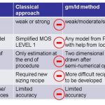
Digital designers have used logic optimization and logic synthesis for decades as a means to produce more optimal designs with EDA tools. On the analog and transistor-level side of design the efforts to automatically optimize for speed or power have generally been limited to circuits with only a handful of transistors. These automated transistor-level optimizations have been improving quite a bit over the past decade, and I attended a webinar today about full-custom, low-power design methodology. The webinar presenter was Michael Pronath. He earned his PhD in Electronics at the Technische Universität München and has worked the past 12 years at MunEDA in Germany.
Optimizing for low-power with transistor sizing has several approaches, here’s the summary comparison between the classical and gm/Id methods:
The gm/Id method is an improvement over the classical approach, yet it still has room for more improvement which was a motivator for MunEDA to develop a numerical sizing approach:
The low-power optimization using numerical sizing is part of an EDA tool called WiCKeD.
Some of the benefits of using this automated transistor-sizing tool:
- >500 devices, >50 variables, >10 specs
- Multi-object optimization
- Supports many specs (transient, noise, pss, pnoise)
- Robust sizing (corners, mismatch)
- Reliability sizing (aging, etc.)
Many analog circuits require the designer to make a trade-off between power and Gain bandwidth (GBW). The following diagram shows how a Pareto curve is used to identify the optimal low-power point for a specific design, where the curve in black is for a nominal process corner and the curve in red shows the design at another process corner.
The theory behind the MunEDA approach for power optimization looks interesting, but who is actually using their tools on real IC designs? The answer is found on a web page listing some 91 customer papers or presentations. In this webinar they summarized five customers:
- Tohoku University – analog design optimization on a pipeline ADC. WiCKeD found lower power consumption, optimized gain, smallest layout area.
- Technical University Dresden – std cell analysis, sense amplifier, clock amplifier.
- Altera – power minimization with multiple Vth MOSFETs in CMOS.
- Fraunhofer – Preamplier for implantable EEG acquisition system.
- Lantiq – nominal vs statistical simulation models, ring oscillator vs technology parameters. Centered their design for yield optimization.
Most webinars that I attend have only a handful of questions, however this webinar from MunEDA had over a dozen questions which really highlights how popular this topic of power optimization is for transistor-level designers.
Webinar Q&A
Q: Your presentation was focused on MOSFET optimization, is the MunEDA solution able to address optimization with non pure CMOS devices, modeled with a custom Verilog-A SPICE model?
Yes, that works.
Q: For only power optimization is there any special feature from WiCKeD?
In DNO you set power to a “min” and keep the other specs in bounds. This setup gives you a power minimization while keeping specs and constraints on all corners.
Q: On slide the WiCKeD GUI appears, and TCL and Python logos were visible. What does it mean, are both languages available?
Yes, both languages are available for batch mode runs.
Q: About the circuit optimization for a given sigma space, is aging also included in that optimization?
Yes, if you have aging models (MOSRA, UDRM or RelXPert).
Q: With respect to Pareto curves in the power/GBW coordinates, the optimum design is selected for FoM = GBW/Power = max? Am I right?
Not exactly. You have two ways: (1) Use linear weights, a*GBW – b*Power = max, or (2) constrained minimization, min Power s.t. GBW=x
Q: Can a dynamic, switched capacitor circuit be optimized as well?
Yes, that is a sweet spot, analytic sizing of switched capacitor circuits can be very hard, but our optimizer handles it well.
Q: A customer test analysis case was done with Tohoku University, a leader in spintronics, do they use your optimizer in spintronic design?
The main application of WiCKeD is in low power CMOS design, which may involve interfaces to spintronic memory elements.
Q: Can WiCKeD handle multiple power/ground domains?
Yes, WiCKeD works on your netlist and feeds it to the simulator. It is very flexible regarding the contents of your netlists and testbenches, simulation algorithms, etc.
Q: Is it possible to watch the presentation again offline?
We will later re-record it in a format suitable for our ELearning platform and make it available there. We will re-run the webinar in June after DAC.
Q: Back to power/ground domains, does that mean that I can have HV and LV devices in the same circuit and WiCKeD will optimize both?
Yes. WiCKeD is routinely applied to I/O circuits such as level shifters. They benefit much from automated sizing.
Q: Speaking about I/O domains, what about ESD devices?
You can include them in your netlist, but I think they are usually not tuned parametrically but rather fixed elements.
Q: Does it give the best Cpk (process capability)? Are the results centered in the process?
There are tools in WiCKeD for yield optimization (although not mentioned in this webinar). This tool can increase Cpk for all specs, including power.
Q: Diffusion resistors at high voltages, can their geometry be optimized considering their voltage coefficients in a switchable (HV+LV) mode of operation or should there be a limited number of use cases specified?
WiCkeD uses schematic properties or netlist instance properties as optimization variables. If the geometry of your diffusion resistor can be set via schematic properties, then WiCkeD can handle it; including callback evaluation to calculate resistor value.
Q: Does the yield optimization account for global, local or both types of variations ?
It is your choice, global/local/both is possible.
Further Reading
MunEDA at DAC
I’ll be visiting with MunEDA at DAC on Monday, June 2nd, their booth is #2213. Let me know if you have any questions that I should ask them.
lang: en_US
Atrenta @ #51DAC Must See!
Last year at DAC, we launched the RTL Signoff platform and our customers responded enthusiastically. We even had a few other EDA companies follow our lead. So what have we been up to since then?
Visit us at DAC this June and learn how we have expanded our industry leading RTL Signoff solutions to handle the next set of challenges in SoC design. Building on the success of our IP Signoff solution, we now offer a unique solution for SoC Signoff. This includes performance and capacity for billion+ gate designs through intelligent abstraction of models. A growing number of SoC design teams have standardized on our solutions and realized significant productivity gains.
Intel’s SoC Challenge!
Innovation is the cornerstone of the semiconductor industry and as history has shown, the majority of semiconductor innovation has come from fabless companies. Apple computer is my favorite example since they went from selling mother boards to computer hobbyists in the 1970’s to being one of the largest and most influential fabless semiconductor companies today.
A Brief History of Chip Design at Apple Computer
Apple is also responsible for some of the most disruptive products including the Macintosh, iPod, iTunes, iPhone, and iPad just to name a few. Apple also set the semiconductor industry on its heels with a 64-bit SoC (A7) inside the iPhone5s. Here is my favorite quote from QCOM:
“I know there’s a lot of noise because Apple did [64-bit] on their A7,” said Anand Chandrasekher, senior vice president and chief marketing officer at Qualcomm, in an interview. “I think they are doing a marketing gimmick. There’s zero benefit a consumer gets from that.”
Mr. Chandrasekher lost his CMO title after that. Even more interesting, he spent his entire career at Intel prior to joining QCOM in 2012 including a five year stint as Senior Vice President of the Intel Mobility Group. And you wonder why Intel missed mobile?
This quote came out later which matches what I heard around Silicon Valley:
“The 64-bit Apple chip hit us in the gut,” said a Qualcomm employee. “Not just us, but everyone, really. We were slack-jawed, and stunned, and unprepared.
Here is QCOM’s formal response:
“The comments made by Anand Chandrasekher, Qualcomm CMO, about 64-bit computing were inaccurate. The mobile hardware and software ecosystem is already moving in the direction of 64-bit. And, the evolution to 64-bit brings desktop class capabilities and user experiences to mobile, as well as enabling mobile processors and software to run new classes ofcomputing devices.”
As soon as the 64-bit A7 news hit, all of the 32-bit SoCs being designed at 20nm were immediately re-architected for 64-bit. From what I know today there will be no 32-bit 20nm SoCs from the big fabless companies. In fact, I would be willing to bet that Apple is the only company shipping a 20nm 64-bit SoC this year. Of course the Intel fan club blames yield for the delay in 20nm SoCs but now you know the truth. Apple disrupted the industry yet again and when you see what the A8 powered iPhone6 is capable of you will be astonished, absolutely.
“To throw good money after bad is to spend more and more money on something that will never be successful.“
This brings me back to Intel’s SoC challenge. There is an interesting presentation titled “Intel’s New Category of SoC Designs, Products” circa 2008. It outlines how Intel is “poised to lead” this category which I find quite interesting. Six years later Intel is still singing the same tune while losing BILLIONS of dollars with little to show for it. This is the most expensive game of “catch-up” that I have ever seen. Meanwhile fabless semiconductor companies like Apple continue to innovate and change the world.
* This is the second of a three part series. Also read Intel’s Manufacturing Lead Explained.
lang: en_US
A Collaborative Approach Yields Better PI for PCBs
The power integrity (PI) of a system is an extremely important aspect to be looked at all levels – chip, package and PCB for overall reliability of the system. At the PCB level, a DC analysis, usually based on IR drop, must ensure that adequate DC voltage, satisfying all constraints of current density and temperature, is delivered to all active devices mounted on the PCB. Similarly an AC analysis must ensure that proper AC current, satisfying all constraints of transient noise voltage levels within the PDN (power delivery network), is delivered to all devices for their proper switching. It’s not as simple as it looks; temperature dependence of metal conductivity brings non-linearity in IR drop analysis. In case of AC analysis, the aspects of frequency dependence, inductance, plane capacitance, decaps (decoupling capacitances), plane-to-plane coupling and resonances, and the like make it much more complex. There are commercial tools available for these analyses which employ multi-physics principles and intensive algorithms for PI analysis at DC as well as AC level. Cadencehas tools such as Sigrity PowerDC, PowerSI and Sigrity Speed2000 (for time-domain analysis). Sigrity OptimizePI is a tool that can be used to reduce the PDN noise by applying suitable decaps.
However, the reason of my pondering over this topic today is for an interesting powerful capability that these tools together offer for front-to-back PCB PI analysis which channelizes the efforts of design engineers, layout engineers and PI analysis expert in the most efficient manner to produce the best results at the most optimized use of resources.
By using Cadence’s Allegro Sigrity PI (which uses constraint-based PI approach for PCB and IC package designs) design engineers at the front-end and layout engineers at the back-end can contribute earlier and more effectively to PCB PI. The DC and AC PI analysis capabilities are in-built for PI optimization and signoff. The constraint-based design methods provide a uniform interface for design-intent information exchange between front-end and back-end.
The Allegro Constraint Manager is used to manage PI constraint sets (PI Csets) for all components. PI Csets contain information for each power rail, including decap component names and quantities, package type, and physical placement guidance. The designers can use Power Feasibility Editor to create PI Csets for components to define their PI design intent. The layout designer gets the information about placement guidance and power rail association for decaps for a reliable placement. The Power Feasibility Editor also provides access to approximate and detailed pre-layout analysis for selection and placement of decaps. In the absence of impedance data from device vendors, high-level specifications can be made to generate target impedance profiles. Sigrity OptimizePI can be used for automatic generation of PI Csets.
[Split-screen view of layout (left) and IR drop analysis results (right)]
For the layout designers to dynamically update metal shapes and vias to address IR drop and current constraint issues, Allegro Sigrity PIprovides access within the layout environment to the setup and result display for DC IR drop and current constraint analyses through split-screen view. This allows layout designers to analyze the situation and identify PI issues much before the PI analysis expert gets involved.
Decap Placement Guidance is a very important feature which can strongly influence the success of AC PI and the routing of wires in general. A decap placed very close to a device can be beneficial for PI, but can restrict routing channels due to decap mounting vias. Similarly, a decap too far from a device can be ineffective in providing switching current to the device and can negatively affect PI. The Sigrity PIprovides a decap placement mode through which a component and a power rail can be selected and then an excellent placement guidance follows with cursor movement, point and click. In the example picture, device to decap distances for top and bottom layers, and decap effective radius (within which the decap will be maximally effective) are shown. The decap value is dynamically computed as the cursor moves.
The overall process makes the design intent and analysis setup information ready for detailed PI analysis by the PI analysis expert. The information about fine adjustments between the front-end and the back-end flows seamlessly for design engineers, layout engineers and PI analysis expert to make necessary updates in their parts and keep them in sync.
Although there are good tools available to serve the purpose of PCB PI analysis, this approach of constraint-based front-to-back comprehensive flow realised by Allegro Sigrity set of tools can be quite effective in terms of resource utilization and quality of results. A more detailed description about the flow and tools can be found in a whitepaperwritten by Brad Brim at Cadence.
More Articles by Pawan Fangaria…..
lang: en_US