
Although MEMS devices in various forms are now found in most electronic devices, predominantly in mobile, automotive, aerospace and many other applications, their major revolution, I believe, is yet to happen. We are seeing rapid innovation in MEMS reflected by their improvements in precision, performance, size reduction, and the continuing evolution of new devices with increasing complexities. The micro level fabrication of MEMS will enable unprecedented use of these into newer and newer semiconductor based electronic devices that will revolutionize the so called IoT arena. MEMS will be essential to IoT products’ ability to connect every aspect of our life, things and happenings around us and provide us ultimate knowledge, control, security through a wide range of devices in many form factors and environments.
The advancement in technology is accelerated when there are supporting tools to accurately model the devices, automate the procedures, quickly simulate, and analyze the designs. I like Coventor’sproducts in catalyzing this race towards reaching the ultimate in MEMS technology; MEMS+ for MEMS+IC design and analysis, CoventorWare for modeling and simulation of MEMS devices and SEMulator3D for process development and virtual fabrication of MEMS and semiconductor devices. I was delighted to look at the new release of CoventorWare 2014 suite that significantly adds into developing new generation of sophisticated MEMS devices. To know more details about the new offering in this release, I had a brief discussion with Steve Breit, VP of Engineering at Coventor. And here is what I learnt about the state-of-the-art new development that happened in CoventorWare 2014.
CoventorWare is a complete suite of tools which allows 2D layout design entry along with process and material information, automatically builds 3D model of a MEMS device, generates mesh, simulates and analyzes to optimize the MEMS device as desired. What we see in CoventorWare 2014 is much improved unique capabilities for high-performance and high-accuracy electro-mechanical and specialty MEMS physics simulations and a novel intuitive interface for fast setup and analysis. The simulators are order of magnitude faster and can handle large meshes on multi-core systems.
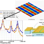
Above is an example of modal harmonic analysis of a specialized PZE (piezo-electric) resonator which is more than 10x faster (with 200 DoF and 88 frequencies) compared to the previous release of Coventorware; the speed-up can further increase with increasing number of DoF (Degree of Freedom) and frequencies. These fast simulations are critical for designing high-Q (Quality Factor) and low-TCF (Temperature Coefficient of Frequency) piezo-mechanical resonators. Similarly other specialized solvers such as PZR (piezo-resistance) for PZR sensors and Reynolds and Stokes solvers for gas damping are available.
CoventorWare provides FEM (Finite Element), BEM (Boundary Element) and also hybrid FEM/BEM methods of simulation for simulating various MEMS physics. The FEM simulations can be used for mechanical analysis including robust contact events whereas BEM simulations can be used for electrostatic actuation and capacitive sensing. The hybrid FEM/BEM approach is used for coupled electro-mechanics, and in CoventorWare 2014 it is 5x faster due to optimization for multi-core systems and a new convergence algorithm.
The new convergence algorithm, ‘Accelerated Coupling’, is available via an intuitive new setup dialog that reduces the number of iterations required for convergence thereby reducing the simulation time.
In order to further enhance user experience in designing increasingly complex MEMS devices, the GUI and user interface has been simplified for all kinds of coupled electro-mechanics along with solver progress reporting on the Job Queue tab. A powerful Python scripting interface has been extended to include mesh and material transforms, making it easy to automate studies of sensitivity to design and manufacturing variables.
Steve summarized by saying that a combination of improvements to simulation performance (which includes multiprocessing, specialized algorithms and optimization of field solvers), user interface enhancements and new scripting support for user convenience has increased user capabilities for efficiently designing and simulating a wide range of MEMS devices with increasing set of parameters for varied applications as per requirement. For example, Gyroscopes can have different levels of bias drift precision depending on their application. While consumer applications are fine with low precision, navigation applications will require very high precision. The Gyroscope designs can be affected with multiple parameters such as bias voltage, electrostatic drive force, and physical effects such as quadrature, thermo-elastic damping and anchor losses. Similarly a varied range of effects must be considered when designing other MEMS devices such as accelerometers, microphones, RF switches & varactors and so on.
It was a very interesting and informative interaction with Steve that enhanced my knowledge about CoventorWare in general and CoventorWare 2014 in particular. It’s worth exploring and using if you are thinking of refining an existing MEMS device or designing a sophisticated new one.
More Articles by Pawan Fangaria…..
lang: en_US