
What if you and I want to exchange encrypted messages? It seems like something that will increasingly be desired given all the NSA/Snowden revelations and all the other snooping shenanigans. The joke going around is that the motto of the NSA is really “Yes We Scan,” which sort of sums it up.
Encryption is essentially scrambling a message so only the intended reader can see it after they unscramble it. By definition, scrambling and unscrambling are inverse (i.e. reversible) processes. Doing and undoing mathematical operations in a secret way that outside parties cannot understand or see is the basis of encryption/decryption.
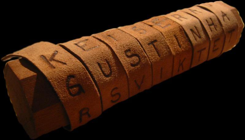
Julius Caesar used encryption to communicate privately. The act of shifting the alphabet by a specific number of places is still called the Caesar cipher. Note that the number of places is kept secret and acts as the key. Before Caesar, the Spartans used a rod of a certain thickness that was wrapped with leather and written upon with the spaces not part of the message being filled with decoy letters so only someone with the right diameter rod could read the message. This was called a skytale. The rod thickness acts as the key.
A modern-day encryption key is a number that is used by an encryption algorithm, such as AES (Advanced Encryption Standard) and others, to encode a message so no one other than the intended reader can see it. Only the intended parties are supposed to have the secret key. The interaction between a key and the algorithm is of fundamental importance in cryptography of all types. That interaction is where the magic happens. An algorithm is simply the formula that tells the processor the exact, step-by-step mathematical functions to perform and the order of those functions. The algorithm is where the magical mathematical spells are kept, but those are not kept secret in modern practice. The key is used with the algorithm to create secrecy.
If a secret key is kept secret, the message processed with that algorithm will be secret from unintended parties. This is called Kerckhoffs’ principle and is worth remembering since it is the heart of modern cryptography. What it says is that you need both the mathematical magic and secret keys for strong cryptography.
Key Agreement
There needs to be a way to exchange the key during the session where the encrypted message is to be sent.
ECDH key agreement, is a way to send the secret key without either of the sides actually having to meet each other. EC stands for elliptic curve that have the property that given two points on the curve (P and Q) there is a third point, P+Q, on the curve that displays the properties of commutivity, associativity, identity, and inverses when applying elliptic curve point multiplication. Point-multiplication is the operation of successively adding a point along an elliptic curve to itself repeatedly. Just for fun the shape of such an elliptic curve is shown in the diagram.
The thing that makes this all work is that EC point-multiplication is doable, but the inverse operation is not doable.Cryptographers call this a one-way or trap door function. (Trap doors go only one way, see?) In regular math, with simple algebra if you know the values of A and A times B you can find the value of B very easily. With Elliptic curve point-multiply if you know A and A point-multiplied by B you cannot figure out what B is. That is the magic.
Now for some Math:
To best explain key agreement with ECDH, let’s say that everyone agrees in advance on a number called G. Now we will do some point-multiply math. Let’s call the sender’s private key PrivKeySend. (Note that each party can be a sender or receiver, but for this purpose we will name one the sender and the other the receiver just to be different from using the typical Alice and Bob nomenclature used by most crpyto books.)
Each private key has a mathematically related and unique public key that is calculated using the elliptic curve equation. Uniqueness is another reason why elliptic curves are used.
If we point-multiply the number G by PrivKeySend we get PubKeySend. Let’s do the same thing for the receiver who has a different private key called PrivKeyReceive and point-multiply that private key by the same numberG to get the receiver’s public key called PubKeyReceive. The sender and receiver can then exchange their public keys with each other on any network since the public keys do not need to be kept secret. Even an unsecured email is fine.
Now, the sender and receiver can make computations using their respective private keys (which they are securely hiding and will never share) and the public key from the other side. Here is where the commutative law of point-multiply will work its magic.
The sender point-multiplies the public key from the other side by his or her stored private key. This is equates to:
PubKeyReceive point-multiplied by PrivKeySend which = G point-multiplied by PrivKeyReceivepoint-multiplied by PrivKeySend
The receiver does the same thing using his or her private key and the public key just received. This equates to:
PubKeySend point-multiplied by PrivKeyReceive = G point-multiplied by PrivKeySend point-multiplied by PrivKeyReceive.
Because point-multiply is commutative these equations have the same value!
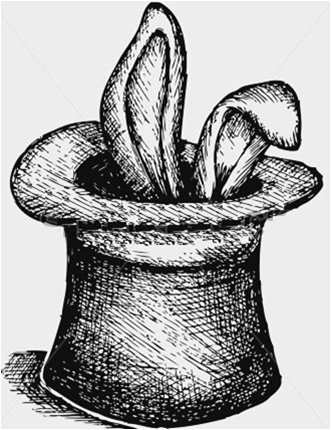
And, the rabbit comes out of the hat: The sender and receiver now have the exact same value, which can now be used as the new encryption key for AES, in their possession.No one besides them can get it because they would need to have one of the private keys and they cannot get them. This calculated value can now be used by the AES algorithm to encrypt and decrypt messages. Pretty cool, isn’t it?
Below is a wonderful video explaining the modular mathematics and discrete logarithm problem that creates the one-way, trapdoor function used in Diffie-Hellman key exhange. (Oh yeah, the “DH” in ECDH stands for Diffie-Hellman who were two of the inventors of this process.)
Bill Boldt, Sr. Marketing Manager, Crypto Products Atmel Corporation

