Designing an SoC sounds way more exciting than bug tracking, but let’s face it – any bug has the potential to make your silicon fail, so we need to take a serious look at the approaches to bug tracking. When using an IP or an IP subsystem in a design, the SoC integrators require some critical knowledge about this IP. The actual design and test files are just one part of that information. It is also very useful to understand all of the outstanding bugs associated with this IP subsystem in real time so that the impact of using a specific version of the IP is clear.
Problems with traditional bug tools
The key problem with this is that most bug tools like Jiraor Bugzilla are project specific. Bugs discovered in IPs developed as part of a bigger system are associated with that system, rather than the IP itself. If that IP is now used elsewhere, there is usually no good way to track open bugs.
Related – IP and Design Management Done Right
The other shortcoming of native bug tools is that bugs cannot be associated with multiple projects or systems. This way, even if the bugs related to an IP were carved out into a separate project, the original project would no longer have access to these bugs.
Many teams have tried to implement IP hierarchy, bug portability, etc. by using custom fields, complex logical associations and call-backs directly in the bug tools themselves. However, IP reuse and IP hierarchy is a dynamic, constantly evolving situation, which makes keeping bug hierarchy and IP reuse in-sync an almost impossibly complex task.
Connecting bugs to an IP management system
Methodics has an approach where the most scalable way to connect bugs to IP is by overlaying IP meta-data in the bug tracking system. Connecting bugs to IP means that the IP management platform itself will understand which bugs are associated with which IP by accessing this metadata. This allows multiple users to view IP bugs directly in their project hierarchy.
Related – Speeding up IP and Data Management
The actual project under which a bug is filed is no longer a limitation. Users can pick the project that they wish (the one they are currently working on) to file a bug. However, the tool allows users to also associate the bug with the IP itself. This allows the IP and IP subsystem hierarchy to be maintained separately in a scalable, fast database, removing the need for the bug tool to track the evolution of the project.
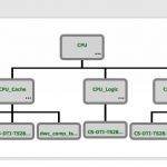
The other advantage of this method is that bugs are visible in the actual hierarchy of the project. For example, take a simple CPU project shown below. In this case, the CPU is made up of three subsystems, which also have additional IP of their own.
In order to make sense of all the bugs associated with each of these components, the user should be able to see the currently open bugs in a similar hierarchy – allowing the user to drill down into each level. A hierarchical bug display looks like:
Bug relationships – discovering predecessors and successors
As an IP develops, some bugs are fixed and others are discovered. Each released version of an IP has a set of outstanding bugs that are open against it.
Related – IP Management Update at DAC
It is quite useful to explore bugs in earlier and later releases of each IP so that the full context of the current IP’s bug profile is visible. This can be done by creating parent-child relationships between IP versions and branches, and having an easy discovery process for these bugs. A snapshot of how this is done is shown below:
Another way these parent/child relationships can be leveraged is between branches of an IP. Bugs found in child branches (variants) can be reflected upstream back to the parent branch (trunk) context and merged into the effective bug list. The same applies for bugs found in the original parent branch, new problems should be communicated to downstream child branches for analysis. Of course, not all of these upstream/downstream bugs are relevant in every context, so the ability to include or dismiss issues is important.
Identifying the context
Another problem with managing bugs in an IP context is understanding at what level to apply the bug. Often the engineer that finds the problem doesn’t have the full context of the hierarchical IP where the problem was found, and the best they can do is to file the issue at the IP hierarchy they have visibility. This leaves the subsystem owner to refile the bug at the appropriate IP further down the hierarchy and a process for managing those changes that communicates with the relevant stakeholders.
Summary
We’ve seen how important it is for bugs to be managed in an IP-centric fashion with modern SoC designs. With IP reuse the norm, bugs must be managed at the resource level rather than the project level and parent child relationships must be tracked to notify downstream/upstream stakeholders when problems occur. Integration people must also have the ability to create placeholder issues at the subsystem they have visibility to and a mechanism for moving those to the appropriate lower level IP when the issue has been properly analyzed.
With these new tools a true IP centric design methodology can be embraced by our SoC design community.