
The semiconductor design industry is ever challenged with increasing chip density, manufacturing complexity with cutting-edge technologies, accommodating multiple IPs with different functionalities from various sources, optimizing power, performance and cost, maximizing manufacturability and reliability and still meeting ever shrinking time-to-market window with good quality and high yield. In such a diverse scenario of conflicting requirements, the business risk is going to only increase. And in the foreseeable future, this trend is going to continue and become harsher; semiconductor industry leaders have no other choice than assimilating diverse expertise and designing more tangled and complicated devices to differentiate and stay profitable in this highly competitive market. Unfortunately, the design tools and flows are also different (which is natural with diversity of expert solutions for particular problems), adding to divergence rather than convergence. So, what are the alternatives to move a design towards faster convergence?
Unity in diversity is the only mantra in such a situation where multiple teams work towards achieving diverse objectives of a design in a short span of time. The whole team has to be brought together (no matter how scattered or culturally different they are across the geography) on a common platform to achieve that common purpose of achieving design closure in the shortest possible time without diverting people from their set objectives. How’s that possible? Remember? I had talked about the “Design Collaboration Solution” in one of my blogon Dassault’sstrategy to move semiconductor design from productivity to profitability. What’s there in it?
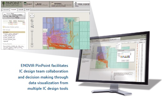
Of course ENOVIA DesignSync has been there for managing large, distributed design data seamlessly from various EDA tools with hierarchical structure supporting IP assembly and re-use and host of other features to make data access efficient and protected through robust control mechanism. Another powerful capability enabling very effective and efficient collaboration among teams and leaders is ENOVIA Pinpoint. It provides graphical analysis of various parts of design, simulation results, test data, critical paths and other design specific data with dashboards for the whole team to take a shared view, assess timelines, identify the diverging paths and resolve by removing constraints or accelerating in particular directions. It provides great predictability in the design schedule and facilitates faster resolution of issues to achieve faster design closure.

ENOVIA Pinpoint by analyzing the diverse design data and bringing them together on a common simple visual dashboard for shared understanding between different tasks across design and verification evangelizes the teams and managers into pro-active thinking; communicating, finding and resolving problems (such as power, heat or timing) before they become critical. The data corresponding to any task can be accessed from central server through links and browsers and re-analyzed by respective design tools.
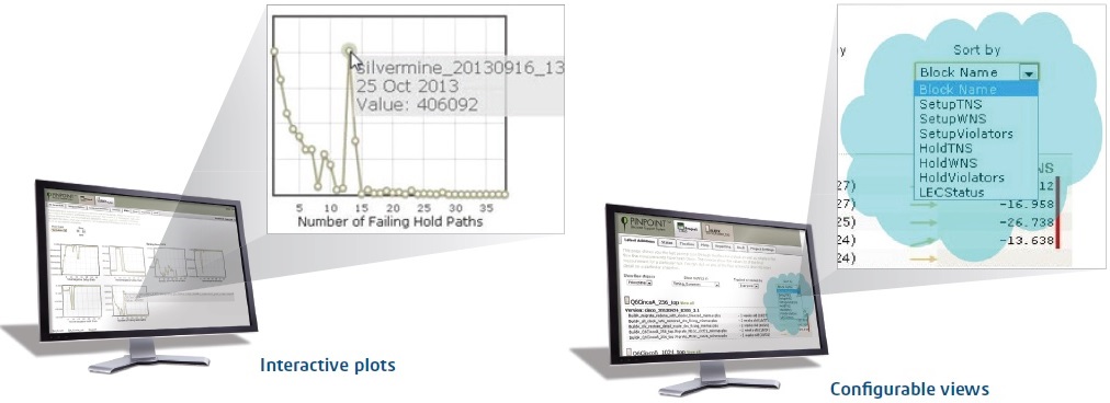
For accessing key data interactions to determine root causes, there is provision for ‘interactive plots’ and ‘configurable views’ to present the most critical data and analyze it to quickly identify outliers. The features include ‘Zoom and Pan’ to visually troubleshoot on the floorplan of the design from top to bottom in the hierarchy.
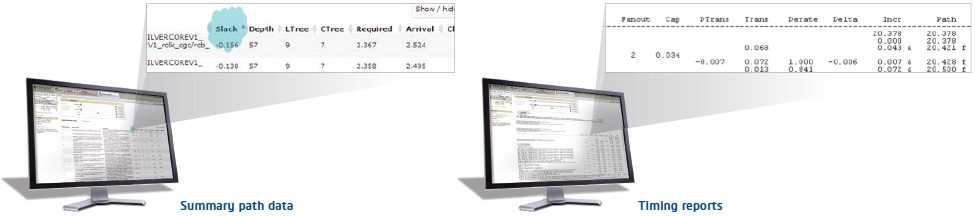
The ENOVIA Pinpoint solution provides multiple design factors such as timing, path and floorplan design which can be reviewed and improved. The floorplan can be superimposed with graphical results of various simulations such as critical paths and power hotspots which can help in taking decisions to improve the floorplan. Similarly, the reports such as ‘summary path data’ and ‘timing reports’ can be reviewed, bottlenecks in timing identified and re-design proposed to improve upon specific path delays.
The ENOVIA Pinpoint has a solid base of ~75 person-years of development and several years of use in semiconductor IC design and production. It’s a knowledge based tool in the sense that it brings attention to priority design issues and produces reports containing objective data, thus defusing tension between different teams or individuals, eliminating distractions due to useless (or subjective) data and keeping the teams focused on their common purpose. Also ENOVIA DesignSync has shown impressive improvements (20% – 74%) in various aspects of collaborative design such as production schedule, quality, IP re-use, multi-site design and productivity.
The Semiconductor Collaborative Design Process and tools from Dassault is being used by more than 120 IC design and development organizations around the world, which includes top 13 semiconductor companies. I love the words of Dwight Galbi of Qualcommwhen he says, “It’s as easy as Google Maps, as the tool zooms down to a single instance, which allows you to diagnose the particular problem. Then you can zoom all the way back out and map all of the failing paths and compare them to your layout.”
More on the Semiconductor Collaborative Design strategy from Dassault can be found in their eBook here. Stay tuned to get more updates on other parts of the entire strategy towards Silicon Thinking Industry Solution Experience.

More Articles by Pawan Fangaria…..
Share this post via:


Consolidation and Competition: Who is Winning the $4.5 Billion Interface IP Race?