webinar IPXACT banner

In-Design DFM Signoff for 14nm FinFET Designs

In-Design DFM Signoff for 14nm FinFET Designs
by Pawan Fangaria on 11-04-2014 at 4:00 pm

While FinFET yield controversy is going on, I see a lot being done to improve that yield by various means. One prime trend today, it must be, it’s worthwhile, is to pull up various signoffs as early as possible during the design cycle. And DFM signoff is a must with respect to yield of fabrication. This reminds me about my patents filed about 6 years ago while I was at Cadence, they dealt with bringing lithography awareness in the design much earlier at the custom floorplanning and layout stage; it might have been too early a methodology to pick up at that time. But now with 14nm and 16nm process nodes and FinFET technology it has become a necessity, that’s my pleasure to feel proud about it 🙂

This day, I am impressed after seeing one of the Samsungpresentations at DACthis year where KK Lin of Samsung tells about Samsung’s readiness with 14LPE and 14LPP technologies and how they have streamlined their process, flow and overall solution to make a design DFM hotspot free for better yield. Samsung is ready with PDKs, libraries, IPs, and design kits for these technologies. After prototyping, the mass production is scheduled by the end of this year. The presentation conveys about their leading 14nm technology which has smallest gate pitch (CPP), innovative constructs for connecting gates in most compact manner and smallest area memory (SRAM) solution. Let’s see their effective and innovating approach for DFM signoff.

In their new DFM solution, Samsung offers DFM kits which can be inserted into design flows, thus enabling designers to seamlessly signoff the design for DFM.

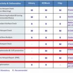
Samsung 14nm DFM requirements are as listed in the above table; some are mandatory and some are recommended for better design differentiation at library, IP and chip level. The Process Hotspot Repair (PHR) and CMP Hotspot Check are mandatory requirements without any tolerance for hotspot.

Samsung uses pattern matching for DFM checking which can represent very complex patterns pretty fast compared to model simulation method; using traditional DRC also can be very complicated with lengthy code writing for this purpose and is not recommended. The pattern matching method provides a viable safety net to capture and repair all known issues from silicon.

The PHR flow is based on CadenceDFM pattern analysis tool, Litho Physical Analyzer (LPA) and integrated with Encounter EDI environment, qualified for 14nm process. The pattern library is created from process hotspot patterns found on wafers. After P&R of design, the patterns are detected using LPA and fixed in the same environment until signoff. Very fast detection and high fixing rate (>95%) has been observed using this flow without any timing impact on the design, thus improving the yield. The minimum set of remaining hotspots is fed-forward to process team for monitoring.

As designers need to see how friendly their design is to fab with respect to CMP, and would need to feed-forward the results to fab, this flow involving calibration for CMP model and prediction of CMP hotspots in the design has been developed by Samsung in collaboration with Cadence. In CMP model validation, it has been observed that actual measurements and simulation results are very closely correlated (~90%) for different step heights, thus increasing the confidence for capturing hotspots.

Very recently, Samsung and Cadence collaborated together to develop a block based analysis flow for designers to run CMP analysis during design implementation and remove CMP hotspots in-design. CMP correction later can be very difficult, time consuming and costly affair. The halo mimics a virtual neighboring environment which is obtained by silicon data analysis, distribution of silicon in terms of density and line width. Reasonable halo conditions are decided for block level simulation. Samsung provides this solution in its CMP model offering.

So, broadly what is done for CMP hotspot detection? Extraction of critical geometry information from design db, analysis of various attributes such as interlayer dielectric (ILD) height & thickness, surface height and Cu thickness, their comparison with the threshold values and identification of hotspots on the chip.

Samsung provides complete package for DFM solution including the kit, model, block level flow and also fixing guidelines based on silicon distribution that includes suggestions such as narrowing, removing, widening or adding dummy patterns among others.

This was a nice learning to know about a differentiated solution for DFM signoff that is Samsung foundry certified with the flow enabled by state-of-the-art tools from Cadence. View the on-line presentation here for more details. Click the link against “Foundry DFM Requirements with Cadence In-Design, Signoff DFM”.

Do we get the desired yield with 14nm FinFET? I think we need to wait until 2015, it’s not too far!

More Articles by PawanFangaria…..


Its a bouncing baby IEEE standard!

Its a bouncing baby IEEE standard!
by Beth Martin on 11-04-2014 at 12:00 am

Pass the cigars! On November 3rd, 2014, the IEEE-SA Standards Board finally approved IEEE P1687 as a new standard. From now on, you can drop the “P” and just call it 1687, or to its friends, IJTAG. Now would be a good time to sign up for an IJTAG technical workshop.

The new IEEE 1687 Internal JTAG (IJTAG) standard is changing the way the industry validates, tests and debugs chips and circuit boards. It builds upon the popular IEEE 1149.1 JTAG board-level test access standard with a set of uniform methods to describe chip internal IP blocks, which are referred to within the standard as “instruments.” IJTAG-based methods are more cost-effective, more accurate, faster and less time-consuming for you than legacy probe-based technologies like an oscilloscope. IJTAG’s software-driven tests and validation routines are initiated from instruments embedded inside chips.

IJTAG is exciting because it addresses the complex issue of testing a heterogenous set of embedded IP. The traditional situation is that the interface for communicating control sequences, and the sequences themselves, are defined by IP developers in a wide variety of different styles with little commonality. Therefore, it falls to the designers to create unique logic to integrate each embedded instrument into an overall design. For SoCs that often have literally hundreds of instruments from a variety of sources with disparate interface styles, this is a major undertaking that typically requires large engineering resource and time. The new IJTAG standard is designed to solve this problem by providing a method for plug-and-play IP integration enabling communication to all the instruments from a single access point (generally an IEEE 1149.1 TAP).

It standardizes a language for describing the IP interface and how IPs are connected to each other. It introduces a new language that defines how patterns that operate or test the IP are to be described. And, there are already automation tools available to simplify the process of connecting any number of IJTAG compliant IP blocks into an integrated network for uniform access and control.

IJTAG has some traction already because it is useful to both IP providers and to chip designers. For IP providers, it makes their products easier to integrate and therefore more attractive to a wider customer base. It also gives them better testing and debugging capabilities as well as an overall more robust product. For chip integrators, the standard also expands the availability of IP sources by eliminating integration uncertainties and incompatibilities as well as provides increased scalability for rapidly growing design sizes.

There’s already been a lot of work with IJTAG. This 2012 whitepaper from Mentor Graphics and NXP Semiconductors details how they implemented P1687 on mixed-signal IPs in a 65 nm automotive design. The results show significant advantages of P1687 over the IEEE 1149.1 (JTAG) test methodology, both in automating the test pattern development and in reducing test setup data volume by more than 50%. The latest news is from Asset Intertech and talks about how interoperability between vendors tools allows IJTAG to be used easily at both chip and board level.

IJTAG is exciting because it addresses the complex issue of testing a heterogenous set of embedded IP. It standardizes a language for describing the IP interface and how IPs are connected to each other. It introduces a new language that defines how patterns that operate or test the IP are to be described. There are tools available to simplify the process of connecting any number of IJTAG compliant IP blocks into an integrated network for uniform access and control. This lets you send commands to the blocks from a single top-level access point (a TAP).

Asset and Mentor have also teamed up to present a series of technical workshops on IEEE 1687 across the world. You can register here.

Has anyone already started using IJTAG? Do you plan to look into it now that the standard is ratified?


Improve Test Robustness & Coverage Early in Design

Improve Test Robustness & Coverage Early in Design
by Pawan Fangaria on 11-03-2014 at 5:00 pm

In a semiconductor design, keeping the design testable with high test coverage has always been a requirement. However with shrinking technology nodes and large, dense SoC designs and complex logic structures, while it has become mandatory to reach close to 100% test coverage, it’s extremely difficult to cope with the explosion of test patterns and keep them robust enough to detect each fault. While at-Speed or transition faults are more cumbersome to detect than stuck-at faults, at deep hierarchical logic levels the circuit becomes hard to test giving rise to another category called random resistive faults. Often a chip fails at the tester due to glitches in the design because of a non-robust test pattern. Trying to understand and correct these glitches can be a very time consuming situation.

Here is an example of the issues with test pattern robustness; while the test pattern generation tool assumes there is only one clock, the clocks merging at the ‘OR’ gate can cause a glitch on the tester. Similarly there can be other issues with deep logic circuits, especially in scenarios which can lead to merging of test clocks, re-convergent resets and so on. These kinds of issues need to be checked and avoided to make the test patterns more robust.

It was a nice occasion attending a webinaroffered by Kiran Vittal, Sr. Director, Product Marketing at Atrenta, where he presented details about SpyGlass DFT and SpyGlass DFT DSM products. These tools can be used very early in the design phase, at the RTL stage, to identify such issues, fix them, verify different aspects, and deliver improved RTL which will provide higher stuck-at and at-speed fault coverage along with more robustness and scannability in the design.

A designer can check for blocks with low coverage in the fault browser, and then a few schematics of the blocks to understand the issues and fix the RTL. The audit coverage report, for both stuck-at and transition faults, provides extremely useful information with existing coverage and actions to be performed to increase that coverage. Recently Atrenta added a smart capability in audit report where it checks for test robustness issues like merging clocks and re-convergent resets and pinpoints these in the report. For example, the various flops which could be the source for glitches are reported. With the help of this report, designers can save significant amounts of time and effort in fixing these issues at RTL, rather than leaving it for the downstream tools to debug later, which can take much longer, weeding through much more detailed data, while using far more expensive tools. A dashboardfor management review is also provided where management can set objectives and criteria to be achieved and then periodically review the progress and trend lines.

SpyGlass DFT identifies the positions in RTL where test points can be inserted to improve controllability and observability of particular nodes. It also reports the number of faults which can be detected after inserting these test points. To fix random resistive issues (described below), SpyGlass DFT DSM can trace throughthe hierarchy and identify test points to be inserted at the block boundaries. The random pattern coverage after applying test points are also generated for ‘what if’ analysis.

Random resistive faults are hard to test, because they are generally buried deep inside the design hierarchy. By zooming on color annotations and displaying the schematic, controllability and observability of nodes, in the range of lowest to highest, can be obtained and appropriate actions can be taken to fix low observability and controllability points. Random resistive faults have high impact on ATPG pattern count and runtime; and ATPG efficiency is especially poor for transition fault detection. SpyGlass DFT DSM reports random pattern coverage estimates in a hierarchical fault browser and helps designers through color annotation in schematics to fix specific faults to increase the coverage.

In an SoC, the DFT architecture can be quite complex and the test logic is controlled by the JTAG TAP controller. SpyGlass DFT runs at block level as well as SoC level and validates block level constraints that must be satisfied at the SoC level. It treats the block as a black box and verifies if correct ‘test mode’ values are reaching the block, thus allowing the processing in a top down manner early in the cycle.

To aid complex initialization with JTAG/IEEE 1500 controllers, SpyGlass DFT provides more effective and easier debugging of test sequences through Tcl commands and assertions. For easy debugging of failed assertions, the logic is highlighted in RTL and the issue is highlighted in the schematic, all in a single GUI. The expanded bit-sequence and waveform view can also be seen. This does not require writing time consuming testbenches; applying structural rules at RTL and some assertions to quickly verify connectivity for different modes of operations are sufficient. Verifying different types of faults and connectivity can be done very early in the design phase.

Another interesting and very effective solution from Atrenta is SoC test signoff with Abstract Modelsof IP which provides significant improvement (~2-6x) in runtime and memory compared to flat flow. SpyGlass also provides automatic insertion of memory test and repair at RTL; it supports vendor independent, user supplied MBIST at RTL.

The RTL test signoff meets many important design requirements such as scannability, stuck-at and transition test coverage goals and test robustness much earlier in the design flow and much faster (~10x faster than post layout). Kiran also talked about a customer case on a mobile application where they achieved ATPG test coverage for stuck-at faults within ~1% of what was reported by SpyGlass at RTL (>99%). The RTL estimation vs. transition ATPG correlation was within ~5%. The average runtime speedup of RTL compared to netlist ATPG was ~30x. View the on-demand webinarposted at Atrenta website to learn more.

More Articles by Pawan Fangaria…..


Let the FinFET Yield Controversy Begin!

Let the FinFET Yield Controversy Begin!
by Daniel Nenni on 11-03-2014 at 8:00 am

It never ceases to amaze me how people point fingers and create controversy to cover their mistakes. It happened at 40nm, 28nm, and again at 20nm and now it is time for the regularly scheduled yield controversy. Of course any conversation about semiconductor yield generates clicks for SemiWiki so I’m happy to play along.

It generally starts with a semiconductor equipment manufacturer missing their quarterly numbers then throwing their customers under the yield bus. Just once I would like to hear a CEO say, “Hey, we missed our number, my fault.” Of course they never name the customer so all customers come under suspicion which is exactly what is happening here. This time it is Art Zafiropoulo, CEO of Ultratech:

As we have discussed on past conference calls, the difficult implementation of 3D FinFET microprocessors to high production manufacturing. Once again a major logic manufacturer delayed their FinFET ramp. We had then requested to prepare LSA tools for shipment for the end of the third quarter which was delayed. These LSA shipments for the most part caused our third quarter revenue to be less than projected. These LSA systems have been rescheduled for shipment in the fourth quarter. Due to the continued low yield in FinFET devices for the past two years, we have seen a reduction in new LSA bookings in subsequent shipments…

I’m very sorry you missed your quarterly number Art and that your stock price is less than half what it was in January of last year. I’m also very sorry you have to blame customers using misleading statements such as this. Ramping leading edge process technologies is more difficult with every new node so delays should be expected. How does a CEO of an equipment manufacturer not know this?

Clearly Art is talking about Intel in regards to 3D FinFET microprocessors for which I understand. Last September Intel CEO BK held up a laptop that was powered by a 14nm CPU and claimed silicon would ship by the end of 2013. That chip is now shipping (about 2 Quarters late) with products due in time for the holiday season. It really is an impressive microprocessor so congrats to Intel on this one:Intel?s 14-nm Parts are Finally Here! | Chipworks Blog

Now check out this interpretation of Art’s comments from the Motley Fool’s “Senior” Technology Specialist:

However, after listening to the earnings call of chip equipment vendor Ultratech (NASDAQ: UTEK ) , it’s clear to me that neither TSMC nor Samsung quite has the FinFET transistor structure (which promises higher performing transistors at lower power) figured out. This, as far as I can tell, strongly suggests that Intel’s manufacturing lead remains intact.

Comparing the TSMC manufacturing capabilities to Samsung’s is absurd. These are two VERY different companies so don’t be a fool and lump them together. This “Senior” Technology Specialist owns Intel stock of course.

An interesting note, when comparing the density of Intel’s 14nm process against TSMC it is always pointed out that 16nm uses the 20nm process with FinFETs instead of planar transistors. When talking about yield however it is not mentioned, especially now that 20nm is in full production with a better than expected yield ramp. Weird hu

Also read: Cliff Hou at TSMC OIP

Here are some FinFET notes from Dr. Mark Liu, president and co-CEO at the TSMC OIP Forum held earlier this month:

  • Today 20nm production has a monthly volume of 60,000 wafers with good defect density
  • The yield learning on 20nm production will directly benefit 16nm production
  • 20nm capacity can quickly support the coming 16nm ramp up
  • More than 90 percent of TSMC’s equipment for the established 20nm node is being reused at 16nm.
  • TSMC’s 16nm defect learning has reached a similar level as 20nm (they are less than six months apart)
  • 10 customer 16nm tape-outs in 2014 so far, more than 45 are expected in 2015
  • TSMC is already in production with a 16nm FinFET network processor for HiSilicon Technologies Co. Ltd.
  • TSMC is ahead of schedule on their 2014 CAPEX

Look at the papers that were presented, they are all about 16nm silicon:

TSMC 2014 OIP – Paper Abstracts

Bottom line:The “major logic manufacturer that pushed out an equipment order” is not TSMC, I’m sure of that. Nor do I think it’s Samsung or Intel as they have already moved 14nm equipment in and are ramping production. If I had to pick one from the other possibilities it would be UMC. They licensed IBM 14nm and I have not heard of any production equipment moving in yet. Just my opinion of course. The truth will come out in 2-3 quarters so lets circle back then and see who is true to their word.

More Articles by Daniel Nenni…..


DAC Deadlines: Action This Day

DAC Deadlines: Action This Day
by Paul McLellan on 11-02-2014 at 7:00 am

DAC is coming up. OK, it’s not actually until next June. It is June 7-11th 2015 at the Moscone Center here in San Francisco. But there are lots of important deadlines coming up for papers, panels and more. The 52[SUP]nd[/SUP] DAC will focus on five key tracks:

  • automotive
  • IP design
  • embedded systems
  • hardware/software security
  • electronic design automation (EDA)

I bet we are going to hear a lot about internet of things (IoT) given those focus areas. Each track will include invited talks, embedded tutorials, special sessions/panels, regular research papers and designer tracks. This is where you come in, because those papers and panels don’t come from nowhere. But you also don’t just hand in something a few weeks before DAC, there are long lead times on various aspects of the conference. You need to get started now.

Research Manuscripts (for the conference itself)
Abstract due before 5pm MT November 21, 2014
Manuscript due 5pm MT December 2, 2014
A DAC research paper explores a specific technology problem and proposes a complete solution to it, with extensive experimental results. Submission includes a six-page paper and a short abstract clearly stating the significant contribution, impact, and results of the submission. Authors are encouraged to submit research manuscripts on all aspects of EDA, embedded systems and software as well as automotive design, hardware and software security, and IP design research topics.

“Work-In-Progress” (WIP) Abstracts
Abstract due before 5:00pm MT, November 21, 2014
Manuscript due 5pm MT December 2, 2014

A DAC work-in-progress provides authors an opportunity for early feedback on current work and preliminary results. Authors have two different opportunities to be part of the Work-in-Progress Poster Session.
Option 1: If authors submit a research manuscript and it is not accepted as part of the regular technical program, there will be a second opportunity to have their submission reviewed as part of the DAC WIP poster session.
Option 2: Authors submit a 100-word abstract and a one-page manuscript to be reviewed as part of the DAC Work-in-Progress Poster session.

Special Session Proposals

Due before 5:00pm MT, November 13, 2014
A special session is devoted to the following topics: traditional core EDA, embedded systems and software (ESS), automotive, security, IP design or a topic of future interest. The topic should be presented from an angle that does not overlap with content from traditional research manuscripts, having a more educational component. A complete submission should list at least three inspiring speakers who address the topic from different viewpoints. The special session submission form is streamlined this year, requiring an overall abstract for the special session plus a title, abstract, and speaker names (and contact info).

Technical Panel Proposals
Due before 5:00pm MT, November 13, 2014
A good panel session explores a single, high-level issue or question with representatives of differing viewpoints. Panel suggestions may include anything that might appeal to the DAC’s broad audience as long as the topic is interesting, timely, informative, and enlightening. The topic should be relevant to one or more segments of DAC attendees. Controversy is appropriate and encouraged.

But wait, there’s more…

Workshop Proposals

Due before 5:00pm MT, November 13, 2014

Co-located Conference Proposals

Proposals due before 5:00pm MT, November 13, 2014

The designer track and the IP track have a little bit more time. More details on these later in the year.

Designer Track
Abstract due before 5:00pm MT, January 20, 2015

IP Track

Abstract due before 5:00pm MT, January 20, 2015

Full details of everything are on the DAC website.


More articles by Paul McLellan…


Semiconductor IP Forecast 2014 – 2020

Semiconductor IP Forecast 2014 – 2020
by Daniel Nenni on 11-01-2014 at 10:00 pm

Given that the majority of my 30+ years in Silicon Valley has revolved around semiconductor IP it should be of no surprise that IP is a big part of SemiWiki and our first book “Fabless: The Transformation of the Semiconductor Industry”. That is also why one of my first round blogger draft choices was IP expert Dr. Eric Esteve. Eric has written 211 IP blogs on SemiWiki thus far garnering close to one million views. Eric had not blogged before SemiWiki but he is the author of the industry standard Interface IP Market Survey which was just updated last month.

According to Eric, Design IP is a niche market worth less than 1% of the semiconductor market but its significance in regards to design enablement is unprecedented. Eric started working in the Interface IP segment in 2005 as marketing director for PLDA. At the same time PLDA was launching the PCI Express gen-1 controller IP and within three years the company revenue multiplied by 3 (PLDA was already 10 years old). Next he worked for Snowbush, the IP division of Gennum, building a five year business plan which required deep knowledge of all protocols (PCI Express, SATA, SuperSpeed USB, HDMI and DDRn). In 2009 Eric started IPnest to better use his IP expertise which was pretty unique at that time. Eric released the first annual “Interface IP Survey and Forecast” in Q2 2009.

Why is this survey unique you may ask? Because you can find information that is not available elsewhere. For example there is an IP vendor ranking by protocol: USB2, USB3, PCIe, DDRn, HDMI, SATA, MIPI, and Ethernet. Eric also compiled a competitive analysis by protocol. For every protocol, you can find price information (for the Controller and for the PHY) and an evaluation of the design start count: the number of PCIe (or USB2, USB3, HDMI etc.) IP sales in 2013, then the total number of ASIC/ASSP design starts that include this protocol. To be able to calculate such a number requires an intimate knowledge of the IP market, absolutely.

Also read:Cliff Hou at TSMC OIP

Before working in the IP business Eric spent 20 years in the ASIC business participating in the IP buying process to support customers and then if you add another 10 years spent essentially on IP you end up with 30+ years of IP experience. During the last five years the Interface IP market segment has doubled in size from $240 million in 2008 to $480 million in 2013. It’s a fast growing market which makes the analysis in this report even more important.

One thing I can tell you is that the foundries rely on this forecast. In regards to the foundation and CPU/GPU IP, the foundries support the IP vendors that their customers work closely with which means TSMC has thousands of IP that needs to be prioritized and silicon proven for the new process nodes.

If you look at IP there is a paradox: Design IP is a niche market, weighing in at $2.5 billion in 2013 which is small if you compare it to the foundry business. But suppress Design IP and probably 70% of the chips processed by the foundries vanishes, which is why foundries take great care in supporting Design IP, and not only hard IP, RTL IP as well. It’s interesting to see that the more successful a foundry is, TSMC for example, the greater care it takes with external IP investing time, money, and resources to make sure the IP ecosystem develops properly. In return, foundry customers can reach production faster which sells more wafers.

After reading the report the only question you will probably have for Eric is this: Is the Interface IP Survey forecast up to 2020 realistic?And the answer is:

“I build a five years forecast since the very first release of the survey. This comes from my experience with Snowbush, as it was one of the key requirements. This year I have based the forecast on the number of commercial design starts (IP sales) by protocols. The first task is to evaluate the TOTAL design starts, and the evolution up to 2020, by protocol. For example, SATA and PCI Express don’t have the same growth behavior, so you need to use the protocol granularity to calculate the ASIC or ASSP design starts. Thus you have to evaluate the pervasion potential for each protocol. Then you have to insert the magic parameter: the “externalization factor”. There is an industry consensus about the fact that IDM and fabless tend to buy certain IP when they used to develop it internally. This is certainly true for Interface IP: this is a standard based IP, it’s pretty difficult for a chip maker to add differentiation. The evaluation is complex, and it’s exactly here that the 30 years’ experience add value! A couple of days ago, I read the first version of the “Interface IP Survey” written in 2009, including a forecast up to 2013. In 2009, I have evaluated the IP market to weight $440 million in 2013. And the result is… $421 million for up-front license only. A forecast with less than 5% error at five years is OK for me!

You can get the latest IP Survey HERE.


What Presentations to Attend During IP-SoC 2014 ?

What Presentations to Attend During IP-SoC 2014 ?
by Eric Esteve on 11-01-2014 at 11:00 am

Will you go to Grenoble next week to attend to IP-SoC? I will do it and will certainly listen to these Keynote Talks:

These keynotes are given by most of the IP vendors leaders: Imagination Technologies, Synopsys, Cadence, Sonics (with the exception of ARM Ltd., I agree). The presentation from STMicroelectronics is expected to clarify a key issue about FD-SOI: can we consider that a solid IP Ecosystem is being built around the technology? As of today, we have posted many articles in Semiwiki, generating an incredible amount of comments (from very positive to neutral, neutral to very critical). Our knowledge of the semiconductor technology has pushed to write very enthusiastic posts. Even if we are not process development specialists, we can understand the major benefits coming from FD-SOI in term of direct wafer cost, low power and indirect cost (by using forward biasing to enhance a slow device instead of trashing it). There is just one step to pass and the technology will become a credible mainstream solution: the creation of a solid IP ecosystem. We expect this presentation to provide the expected answers about the FD-SOI IP Ecosystem.

The keynote from Mark Ma (who organizes IP-SOC in Shanghai on top of running Jiatao, an IP rep in China) will be interesting to listen as well. We know that Chinese SC companies are rocketing, trying to serve a domestic market which is still dominated by alien chip vendors, but we expect to get many more information, and to learn about the IP market in China. How many local suppliers? Is it also dominated by the big guys, or do we see Chinese suppliers for CPU or GPU IP?

Don’t forget to listen to the Invited Talks,I have picked two of these:

In the first talk, Gabriele Saucier will speak about a Design&Reuse facet that you probably ignore, the IP management tool develop by D&R and sold to (very) big names of the electronic industry like some large European Telecom companies, or a very successful American OEM (sorry but I can’t share the name, but it’s BIG!).

I will certainly attend to the second as I will give a presentation, updated from this given at CDN-Live this year as I will provide additionnal information about the Design Starts by protocol. I will review the Winners (rather protocols than IP vendors, even if I will propose a ranking by protocols)… and the Losers (once again talking about protocols or technologies rather than dropping vendor names). I welcome your questions during the presentation!

Let’s finish with the two Panels:

  • IoT Wonderland for IP based Electronic Systems” with the participation of Drew Wingard (Sonics), Michel Depeyrot (Dolphin Integration), Nikos Zervas (CAST), John Koeter (Synopsys), Eklovya Sharma (Sibridge Technology), Ian Dennison (Cadence Design Systems)
  • What is the most efficient distribution scheme for an IP Providers and IP Consumers?” organized by Gabrièle Saucier (Design And Reuse) with the participation of Harold Barbour (CAST), Sébastien Rabou (Barco Silex), Howard Pakosh (Chipstart), Nigel Dixon (T2M UG), Mark Ma (Shanghai Jiatao Industrial Corp Ltd), Sanjeev Sharma (Terminus Circuits), Amir Bar-Niv (Cadence Design Systems)

I will tell you more after IP-SoC, as it’s difficult to foresee the quality of a panel: it’s all about discussion, interaction and questions from the audience!

See you on Wednesday 5[SUP]th[/SUP] November in Grenoble at 9am!

From Eric Esteve from IPNEST


Noise & Reliability of FinFET Designs – Success Stories!

Noise & Reliability of FinFET Designs – Success Stories!
by Pawan Fangaria on 11-01-2014 at 7:00 am

I think by now there has been good level of discussion on FinFET technology at sub-20 nm process nodes and this is an answer to ultra dense, high performance, low power, and billion+ gate SoC designs within the same area. However, it comes with some of the key challenges with respect to power, noise and reliability of the design. A FinFET typically operating at lower supply voltage and higher drive strength reduces noise margin and increases transient noise. The higher current density (~25% more with a typical FinFET transistor) in smaller fragile interconnects of a dense design severely impacts electro migration (EM) making EM sign-off critical. Additionally the fin structure of FinFET provides little space for heat to escape, thus leading to heat accumulation and further impacting EM and ESD (Electrostatic Discharge). Also, higher gate count and additional metal layers significantly increase simulation runtime and memory requirements, especially for full-chip analyses (with package and PCB data for better accuracy). In order to tackle these issues, multiple methods / engines with silicon level accuracy (involving multi physics simulations) along with smart computational algorithms to tackle large sizes of designs (including package and system information) must be used.

Upholding these requirements, ANSYShas added new capabilities in its production proven (with thousands of designs into successful silicon) RedHawk platform to include FinFETs and 2.5D/3D ICs with TSVs (through-silicon vias).

To tackle high capacity and high performance, RedHawk’s DMP (Distributed Machine Processing) technology smartly distributes a design database across a network of machines where each machine analyzes a portion of the design within the context of the entire chip including package, thus providing flat sign-off accuracy at enhanced performance and reduced memory per machine for full-chip voltage drop, EM and ESD analyses.

RedHawk employs state-of-the-science engines to meet these challenges of next generation SoCs; an integrated solver as transient simulation engine that can handle 2 B+ node of RLC network matrices along with distributed and cross-coupled package models; a high performance ALP3D solver for power up (rush current) analysis in complex power gate architectures. An engine to support stacked-die structures allows simulation of heterogeneous designs where each die and interposer can be based on different process technologies. Apache Power Library (APL) remains a fundamental underlying technology through its ability to capture nonlinear behaviour of circuit elements into compact, linear models that enable full-chip simulations while achieving sign-off quality results comparable to Spice. RedHawk handles ever increasing complex EM rules and quickly identifies EM hotspots related to power and signal wires as well as ESD failures.

RedHawk uses APL and Custom Macro Model (CMM) to incorporate device-level RC parasitics and switching current waveforms for full-chip transient simulation at pico-second resolution that provides Spice level sign-off accuracy. It simulates all power and ground domains simultaneously to accurately predict the current drawn and voltage seen at every cell in the design, and noise coupling that can happen inside the chip. At sub-20nm, for FinFET based designs, the modeling, extraction and analysis capabilities are expanded to support special metal layers, complex via structures, dummy devices, vertical resistances and double patterning.

RedHawk-CPA (in RedHawk 2014 release) accurately analyzes the effect of package parasitics on dynamic voltage drop which takes into account the current flow inside the package and bumps, necessary for increasing accuracy levels at advanced nodes and FinFET based designs. It provides comprehensive chip-package sign-off through its integrated extraction, model hook-up, and co-simulation capabilities. Its 3D FEM solver uses package layout and material property to generate a detailed per-bump parasitic network model that is appropriate for time-domain simulations. RedHawk-CPA enables seamless merging of fully distributed package parasitic network (that provides increased granularity and accuracy) with the on-die PDN. It displays both the chip and the package layouts and analysis results, enabling co-analysis, debug and simultaneous optimization.

RedHawk’s current flow-aware extraction techniques help in achieving sign-off quality results for every wire and via that enable in accurate analysis of EM violations on power/ground and signal lines. PathFinder supports IP and SoC level ESD integrity analysis by providing connectivity as well as interconnects failure checks for all current flow pathways from an ESD event (HBM or CDM).

As discussed earlier, heat generation and trapping in a FinFET based design can significantly impact lifetime of the device. ANSYS’s comprehensive chip-package-system thermal analysis flow takes in chip data along with package and system to generate accurate on-chip thermal profiles which are used by RedHawk to enable thermal-aware EM and ESD analysis. A Chip Thermal Model (CTM) created using temperature-aware power density and package thermal boundary conditions from a system simulation enables required thermal integrity for FinFET and 3D ICs.

ANSYS solution provides best coverage of power integrity and reliability verification for RTL to GDS power noise closure with and without input vectors. PowerArtist enables a physical-aware RTL design for power methodology that creates RPM (RTL Power Model) of a given design. RedHawk’s VectorLessengine along with logic simulation (using RTL VCD), state propagation (using activity) and gate level VCD simulation engines enable a comprehensive analysis toolkit for dynamic power noise. It can work in mixed-mode, for example with one block having gate level VCD, another having RTL vectors and rest of the design using VectorLess engine to generate the overall switching scenario. RedHawk provides enhanced capabilities to accurately simulate an on-chip LDO (low-dropout regulator) during full-chip static and dynamic simulations enabling sign-off confidence.

For easy and flexible analysis of results and comprehensive debugging (identifying design weaknesses and their fixes), RedHawk provides multi-tab, multi-pane GUI which allows simultaneous display of multiple results and tables, and multiple chip layouts with their own power densities and impact on each other.

Ansys’s power noise and reliability solution also includes production proven system-level simulation solutions: SIWave for signal integrity, Icepak for thermal integrity and HFSS for EMI and high frequency analysis.

ANSYS provides most comprehensive platform for system-aware chip simulation as well as chip-package-aware system simulation. Read the whitepaperposted at ANSYS website to know more details about each of these capabilities.

RedHawk is certified for 16 nm FinFET based design sign-off by TSMCand Tri-Gate based design reference flow at 14nm by Intel. These foundry certifications along with substantial successful production with ANSYS solutions provide increased confidence in these advanced technologies. Read more on the certifications here –
Intel & ANSYS Enable 14nm Chip Production
ANSYS Tools Shine at FinFET Nodes!

A recent success story of chip production with ANSYS power, noise and reliability solution was at NXPwhere a complex RF-CMOS IC has shown very good correlation with simulation results. To know more about how they have used ANSYS tools for this IC, attend a free webinarto be presented by NXP, here is the schedule –

Webinar: Noise coupling analysis for advanced mixed-signal IC’s
Date: Tuesday, November 4, 2014 – 8:00am – 9:00am PST
Location: Online
Register here

More Articles by PawanFangaria…..


Debugging a 10 bit SAR ADC

Debugging a 10 bit SAR ADC
by Daniel Payne on 10-31-2014 at 4:00 pm

SMIC (Semiconductor Manufacturing International Corporation) is a China-based foundry with technology ranging from 0.35 micron to 28 nm, and we’ve blogged about them before on SemiWiki. I’ve been reading about SMIC recently because they created a technical presentation for the MunEDA Technical Forum Shanghai in March. They will also present this at the MunEDA User Group meetingon Nov 17-18 in Munich, Germanywith the title: SAR ADC Debug Using WiCkeD. The acronym SAR ADC means Successive Approximation Register, Analog to Digital Converter. These converter circuits accept an analog input, then create a precise digital value output at a certain sampling rate and resolution of bits. Other types of converter architectures are: pipeline, flash and sigma-delta ADCs.


Simplified N-bit SAR ADC Architecture

A customer design fabricated at SMIC in 40 nm technology contained a 10 bit SAR ADC with low performance yield, so SMIC engineers set about to debug the source of the low yield and improve it. The ADC was producing wrong code conversion values and only reached an Effective Number Of Bits (ENOB) of 6, instead of the intended 10. Running a full SNDR (Signal to Noise plus Distortion Ratio) simulation on this circuit with 3,500 devices required tens of hours, so was not deemed efficient for debug purposes.


Low performance yield with ENOB of 6, instead of 10

Related – Transistor-level Sizing Optimization

To debug this low yield issue they used an EDA tool from MunEDA called WiCkeD where the debug flow is based upon using a fail pattern and testbench:

Differential Nonlinearity (DNL) error is defined as the difference between an actual step width and the ideal value of 1 LSB (Least Significant Bit).


DNL must be less than 1 LSB for no missing codes

Next, a large number of key devices were selected to see how they impacted deviation values while varying values of Vin. Results from the key devices finding showed that devices in the capacitor array had the greatest impact on deviation, followed by devices in the second stage comparator, and finally devices in the first stage comparator.

Mismatch analysis was run on sub-blocks independently to identify sensitive blocks before analyzing single devices. This hierarchical approach greatly reduces the simulation effort.

Related – An IO Design Optimization Flow for Reliability in 28 nm CMOS

Plots were made to show the distortion behavior of each device to see if correlation was negative or positive:


Device variation, the deviation value for code 496 caused by distortion is negative correlated


Device variation, the deviation value for code 504 caused by distortion is positive correlated

While verifying the size parameters and process parameters it was found that the MOM (Metal Oxide Metal) capacitor’s mismatch was the main cause of distortion. So by changing the mismatch variation in the MOM capacitor the simulated value for ENOB improves from 6 (Red) to 9 (Green):


ENOB improvement by modifying the mismatch variation of MOM capacitor

Conclusion

A 10 bit SAR ADC with low yield was debugged using the WiCkeD tool to pinpoint the source of deviations. Reducing the mismatch variation of MOM capacitors in simulation increased ENOB significantly, proving that the issue was actually caused by the local variation of these devices. The SMIC debug strategy was based on the designer’s circuit knowledge, and enabled by MunEDA’s flexible, interactive analysis tools.

To view the 19 page presentation by SMIC, request it online.


GNSS, dead reckoning, and MEMS IMUs

GNSS, dead reckoning, and MEMS IMUs
by Don Dingee on 10-31-2014 at 4:00 pm

GNSS is a wonderful invention, and low cost receivers have crept into smartphones and other mobile devices. However, GNSS does not solve all problems, especially in urban environments. The canyon effect blocks signals at street level between tall buildings, and signals do not penetrate to the interior of parking garages, tunnels, basements or lower floors of large structures. Continue reading “GNSS, dead reckoning, and MEMS IMUs”