As we are seeing more and more automation in most of our activities, not only through software but also smart electronics (at cutting-edge technologies) equipped with processors, micro-controllers, sensors and so on which make a whole system as an integrated entity on a small piece of semiconductor intertwined with other systems to accomplish various tasks, there is a growing need to consider and optimize (Power, Performance, Area, …) the whole system together and make it robust and reliable to avoid any silicon failure over its lifetime. Since ANSYSspecializes in offering solutions for power, noise and reliability management in electronic and semiconductor systems, it was a nice gesture from ANSYS organizing an Electronics Simulation Expo (AESE) in Bangalore where they invited the electronic and semiconductor community from this part of the world (the world today is globally connected though) to present their views on improving electronic system design through sharing of design and simulation best practices.
I had a great conversation with Jai Pollayil, Director Applications Engineering at ANSYS and his team at Bangalore and was very positively influenced with the success of AESE. It was impressive to know there were about 300+ registrations and more than 50% of that in controlled attendance at this first instance of AESE; that confirms about the pace of electronics and semiconductor design development in India and the world over. Some glimpses about this Expo are here –
[Sudhir Sharma, Global Industry Director at ANSYS, addressing the audience]
Sudhir Sharma, Global Industry Director at ANSYS welcomed the audience and provided a brief introduction about the day long program.
[Jagan Ayyaswami, Director Engineering at Qualcomm, presenting the keynote address on IoT]
Jagan Ayyaswami, Director Engineering at Qualcommpresented the Customer Keynote and spoke at length on the trends, opportunities, challenges and future of Internet of Things (IoT) which is driven by electronics and internet.
Internet and Mobile (which drive electronics business) are the most rapidly growing area in the world, connecting other devices together. Between 2003 and 2010, while world population has increased from 6.3 Billion to 6.8 Billion, the number of connected devices has increased from 500 Million to 12.5 Billion. And it is expected that the number of connected devices will grow to 50 Billion by 2020 at the expected population of 7.6 Billion by then; that means ~7 devices per person! What does that foretell? Everything will be smart in the world with smart appliances, smart home, smart meters, smart automotive, smart city and smart personal electronics including health, fitness and medicine. How will it be accomplished? With IoT, smart communication between electronic devices through internet, entering every domain of our life including industrial, personal, education, business, communication, management, and entertainment and so on. Of course there are challenges such as security, privacy, energy sourcing and efficiency, governance, and common standards, interoperability and protocols etc. which need to be addressed, there is huge opportunity going forward. And number of internet users in India is growing rapidly making the electronics and semiconductor design business in India much attractive.
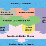
The ANSYS Technical Keynote was presented by Aveek Sarkar, VP Technology Evangelism at ANSYS in which he, very rightly, emphasized on the need for analyzing an electronic system as a whole to ensure its robust, optimized and reliable design and how ANSYS solutions can help meeting these objectives.
With the whole electronic system as the focus, the technical paper presentations were well organized into two parallel tracks – i) Package / PCB and ii) IC / Semiconductor. There were great presentations from key players in the industry including Intel, Qualcomm, Dell, Broadcom, AMD and others. While I will specifically talk about a few of them later, the key messages which were coming out from expert designers who presented were – i) Power has become a key criteria and needs to be looked at from whole system perspective, ii) Reliability is at stake at advanced nodes and needs careful handling, iii) The design sizes are growing ultra-large and those need high capacity and high performance solutions, iv) Need for faster design (chip + package) convergence with wider coverage and accuracy. It will be interesting to know about how these problems are being solved in these design houses by using ANSYS tools & technologies. Stay tuned!