The predominant model for IoT sensor data flow is for data collection on the device and data storage, analysis and access in the cloud. By cloud, I mean that particular vendor’s servers. This is true for Fitbit, Nest, Dropcam,Trace Snow (my favorite skiing app), Smart Things, etc. If you look up IBM’s presumptuously named Internet of Things Foundation, you will see that it is mainly an effort on their part to drive adoption of their cloud backend for IoT applications. The same is true for the Intel push with Edison. The development kit includes access to the Intel Cloud-based Analytics service. It’s understandable that the cloud can be used for heavy lifting with IoT applications. But the cloud can also be used to lock in customers and block competition. I took a quick look at the websites for several prominent IoT devices and they all offer an API for linking devices. This is good. So for instance, when I go hiking I can connect my Fitbit to my Endomondoand get improved information about my activity. Fitbit tracks my steps, but has no GPS. Endomondo is an app on my phone that can tell me my route, distance, elevation, etc. Together I can get a better picture of my activity. However when I have my Fitbit right next to my phone it seems counterintuitive that I cannot sync it unless I have an internet connection. With all of these devices being dependent on the vendor cloud service, we are subject to their reliability and even to their very existence. If one of the above companies were to close their doors, I’d have a ‘brick.’ This is close to what is happening to the buyers of the Revolvhome automation hub after the company was bought by Google/Nest. This raises the existential question of who ‘owns’ the device. What if they decide I have violated their terms of service? Can they unilaterally cause my device to become a lump. Kai Kreuzer, project lead of the Eclipse Smart Home Project, has an excellent slide that illustrates the present situation. When it comes to your house, odds are that you will have multiple vendors providing the devices. I have a wifi-connected stereo receiver with airplay. My TV has Wifi and an app. If I add smart lights, a Nest thermostat, security webcams, alarm system, garage door opener and other things, I most certainly will have an interoperability problem. Estimates are that our houses will have hundreds of connected things in the not too distant future. Major manufacturers are already producing these products in volume. You can find them at Home Depot, Lowes and online. Lowes even has its own line of home control products called Iris. Some of the companies manufacturing smart home products include big names like Philips, GE, Leviton, and Schlage. These are light bulbs, wall switches, door locks, water flow sensor, leak detectors, motion sensors, etc. The list goes on, with more coming every day. There are standards for these home automation devices such as Z-Wave, or ZigBee, but things are still in the early days. We also have Insteon, wifi based devices such as WeMo and more. Most these devices come with their own app or remote control, and probably an internet based service. There is a movement to consolidate these with hubs. The most common of them are made by Smart Things or Wink. Even the office supply company Staples offers one. And they mostly also use a cloud based service provided by their vendor. One notable exception is the very successful Kickstarter project called the NEEO. With the cloud based hubs, there is still concern for availability, security, and privacy. Let’s say your internet connection fails or the hub vendor has an outage, your security system will be off line or your door locks won’t be accessible. These systems know when you are home and away. If Wink or Smart Things has a security breach, then hackers could find out when you are not home. And, incidentally the only way you will find out if they have a security breach is if they tell you about it. There is a grass roots initiative to provide local control for these devices and systems. This is analogous to what happened with computer hardware and operating systems. We are witnessing a recapitulation of these earlier technology waves. The advocates of open and locally controlled devices such as Kai Kruezer, argue that innovation is fueled by open systems. He started the OpenHAB project, which stands for Open Home Automation Bus. It is a software package that can run on an open hardware platform like the Raspberry Pi. It is gaining momentum, but is not anywhere near to being a consumer option yet. OpenHAB has spawned the Eclipse Smart Home project. Many software developers are familiar with the Eclipse Foundation as an organization that facilitates major open source software development tools and projects. OpenHAB and the Eclipse Smart Home project will be very important for the future of the Internet of Things. Kai Kreuzer has a slide that calls for an Intranet of Things. Then cloud can then be used for things like back up and for providing off site connectivity where it is called for and makes sense. They are proposing a software architecture and helping to build a portable stack based on it. It will allow new devices to be easily integrated. Around these devices there will be code to support events from sensors. There are four components in the Eclipse Smart Home architecture: connectivity, automation, user interfaces and persistence. Hackers, makers and home hobbyists are already busy applying OpenHAB. They are using open source hardware and radios to build their own hubs. There is even one enterprising hacker who figured out how to root the low cost cloud based Wink hub and replace its firmware with the OpenHAB code. The Wink hardware has a compact package that includes a processor along with WiFi, ZigBee, Z-Wave interfaces. We are in the pioneering days of this technology and it will serve us well to question the architectures that businesses are promoting. If consumers ask for local control of their devices they can push the industry in that direction. Hopefully the traditions of open hardware and software will prevail, like it has for the PC and for Linux.

10 Cyber Security Predictions for 2015!
In 2014 worries about security went from a simple “meh” to “WTF!” Not only did high-profile attacks get sensational media coverage, but those incidents led to a pivotal judicial ruling that corporations can be sued for data breaches. And as hard as it is to believe, 2015 will only get worse because attack surfaces are expanding as mobile BYOD policies overtake enterprises, cloud services spread, and a growing number of IoT networks get rolled out. Add m-commerce, e-banking, and mobile payments to the questionable tradition of lax credit card security infrastructure in the U.S. and you get a perfect storm for cybercrime.
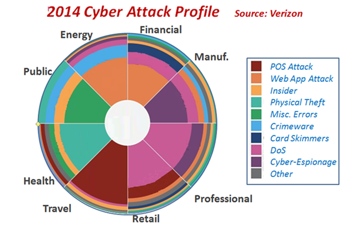
In fact, 92% of attacks across the range of segments come from nine basic sources (seen in the diagram below), according to Verizon. More numerous and sophisticated cyber crimes are anticipated for this year and beyond.
1. More companies to get “Sony’d”
2014 saw the release of highly-evolved threats from criminals that in the past only came from governments, electronic armies and defense firms. A wide-range of targets included organizations in retail, entertainment, finance, healthcare, industrial, military, among countless other industries. As a repeat offender, Sony is now the cyber-victim poster child, and the term “Sony’d” has become a verb meaning digital security incompetence. Perhaps Sony’s motto should be changed from “make.believe.” to “make.believe.security.” Just saying!
Prior to 2014, companies on a wholesale basis tended to simply deny cyber vulnerabilities. However, a string of higher profile data breaches — such as Sony, Heartbleed, Poodle, Shellshock, Russian Cyber-vor, Home Depot, Target, PF Chang’s, eBay, etc. — have changed all of that. Denial is dead, but confusion and about what to do is rampant.
2. Embedded insecurity rising
Computing naturally segregates into embedded systems and humans sitting in front of screens. Embedded systems are processor-based subsystems that are “embedded” into other machines or bigger systems. Examples are routers, industrial controls, avionics, automotive engine and in-cabin systems, medical diagnostics, white goods, consumer electronics, smart weapons, and countless others. Embedded security was not a big deal until the IoT emerged, which will lead to billions of smart, communicating nodes. 15 to more than 20 billion IoT nodes are being forecast by 2020, which will create a gigantic attack platform and make security paramount.
A recent study by HP revealed that 70% of interconnected (IoT) devices have serious vulnerabilities to attacks. The devices they investigated consisted of “things” like cloud-connected TVs, smart thermostats and electronic door locks.
“The current state of Internet of Things security seems to take all the vulnerabilities from existing spaces – network security, application security, mobile security and Internet-connected devices — and combine them into a new, even more insecure space, which is troubling,” HP’s Daniel Miessler stated.
Issues HP identified ranged from weak passwords, to lack of encryption, to poor interfaces, to troubling firmware, to unencrypted updating protocols. Other notable findings included:
- 60% of devices were subject to weak credentials
- 90% collected personal data
- 80% did not use passwords or used very weak passwords
- 70% of cloud connected mobile devices allowed access to user accounts
- 70% of devices were unencrypted
Investigators at the Black Hat Conference demonstrated serious security flaws in home automation systems. At DEFCON, investigators hacked NFC-based payment systems showing that passwords and account data was vulnerable. They also revealed that the doors of a Tesla car could be hacked to open while in motion. Nice! Other attacks were exploited on smart TVs, Boxee TV devices, smartphone biometric systems, routers, IP cameras, smart meters, healthcare devices, SCADA (supervisory, control and data acquisition) devices, engine control units, and some wearables. Even simple USB firmware was proven to be highly vulnerable… “Bad USB.”
These are just the tip of the embedded insecurity iceberg. Under the surface is the entire Dark Net which adds even more treacherousness. Security companies like Symmantic have identified home automation as a likely early IoT attack point. That is not surprising because home automation will be an early adopter of IoT technologies, after all. In-house appliances also represent an attractive attack surface as more firmware is contained in smart TVs, set top boxes, white goods, and routers that also communicate. Node-to-node connectivity security extends to industrial settings as well.
Tools like Shodan, which is the Google of embedded systems, make it very easy for hackers to get into the things in the IoT. CNN recently called Shodan the scariest search engine on the Internet. You can see why since everything that is connected is now accessible. Clearly strong security, including hardware-based crypto elements, is paramount.
3. More storms from the cloud
It became clear in 2014 that cloud services such as iCloud, GoogleDrive, DropBox and others were rather large targets because they are replete with sensitive data (just ask Jennifer Lawrence). The cloud is starting to look like the technological Typhoid Mary that can spread viruses, malware, ransomware, rootkits, and other bad things around the world. As we know by now, the key to security is how well cryptographic keys are stored. Heartbleed taught us that, so utilizing new technologies and more secure approaches to maintain and control cryptographic keys will accelerate in 2015 to address endemic cloud exposure. Look for more use of hardware-based key storage.
4. Cyber warfare breaks out
eBay, PF Chang’s, Home Depot, Sony, JP Morgan, and Target are well-known names on the cybercrime blotter, and things will just get worse as cyber armies go on the attack. North Korea’s special cyber units, the Syrian Electronic Army, the Iranian Cyber Army (ICA), and Unit 61398 of the People’s Liberation Army of China are high profile examples of cyber-armies that are hostile to Western interests. Every country now seems to have a cyber-army units to conduct asymmetric warfare. (These groups are even adopting logos, with eagles appearing to be a very popular motif.)
Cyber warfare is attractive because government-built malware is cheap, accessible, and covert, and thus highly efficient. Researchers have estimated that 87% of cyber-attacks on companies are state-affiliated, 11% by organized crime, 1% by competitors, and another 1% by former employees. Long story short, cyber war is real and it has already been waged against non-state commercial actors such as Sony. It won’t stop there.
5. Cybercrime mobilizes
According to security researchers, mobile will become an increasingly attractive target for hackers. Fifteen million mobile devices are infected with malware according to a report by Alcatel-Lucent’s Kindsight Security Labs. Malvertising is rampant on untrusted app stores and ransomware is being attached to virtual currencies. Easily acquired malware generation kits and source code make it extremely easy to target mobile devices. Malicious apps take advantage of the Webkit plugin and gain control over application data which hands credentials, bank account, and email details over to hackers. What’s more, online banking malware is also spreading. 2014 presented ZeuS, which stole data, and VAWTRAK that hit online banking customers in Japan.
Even two-factor authentication measures that banks employ have recently been breached using schemes, such as Operation Emmental. Emmental is the real name of Swiss cheese, which of course is full of holes just like the banking systems’ security mechanisms. Emmentaluses fake mobile apps and Domain Name System (DNS) changers to launch mobile phishing attacks to get at online banking accounts and steal identities. Some researchers believe that cybercriminals will increasingly use such sophisticated attacks to make illegal equity front running and short selling scams.
6. Growing electronic payments tanatalize attackers
Apple Pay could be a land mine just waiting to explode due to NFC’s susceptibility to hacking. Google Wallet is an example of what can happen when a malicious app is granted NFC privileges making it capable of stealing account information and money. M-commerce schemes like WeChat could be another big potential target.
E-payments are growing and with that so will the attacks on mobile devices using schemes ranging from FakeID to master key. Master key is an exploit kit similar to blackhole exploit kit that specifically targets mobile, where FakeID allows malicious apps to impersonate legitimate apps that allow access to sensitive data without triggering suspicion.
7. Health records represent a cyber-crime gold mine
Electronic Health Records (EHR) are now mandatory in the U.S. and a vast amount of personal data is being collected and stored as never before. Because information is money, thieves will go where the information is (to paraphrase Willie Sutton). Health records are considered higher value in the hacking underground than stolen credit card data. Criminals throughout both the U.S. and UK are now specializing in health record hacking. In fact, the U.S. Identity Theft Resource Center reported 720 major data breaches during 2014 with 42% of those being health records.
8. Targeted attacks increase
Targeted attacks, also known as Advanced Persistent Threats (APTs), are very frightening due to their stealthy nature. The main differences between APTs and traditional cyber-attacks are target selection, silence, and duration of attack. According to research company APTnotes, the number of attacks by year went from 3 in 2010 to 14 in 2012 to 53 in 2014. APT targets are carefully selected, in contrast to traditional attacks that use any available corporate targets. The goal is to get in quietly and stay unnoticed for long periods of time, as seen in the famous APT attack that victimized the networking company Nortel. Chinese spyware was present on Nortel’s systems for almost ten years without being detected and drained the company of valuable intellectual property and other information. Now that’s persistent!
9. Laws and regulations try to play catch up
A number of cyber security laws are being considered in the U.S. including the National Cybersecurity Protection Act of 2014, which advocates the sharing of cybersecurity information with the private sector, provide technical assistance and incident response to companies and federal agencies. Another one to note is the Federal Information Security Modernization Act of 2014 that is designed to better protect federal agencies from cyber-attacks. A third is the Border Patrol Agent Pay Reform Act of 2013 to recruit and retain cyber professionals who are in high demand. Additionally, there is the Cybersecurity Workforce Assessment Act, which aims to enhance the readiness, capacity, training, recruitment, and retention of the cybersecurity workforce. President Obama stated that wants a 30-day deadline for notices and a revised “Consumer Privacy Bill of Rights.”
One of the more interesting and intelligent recommendations came from the FDA, who issued guidelines for wireless medical device security to ensure hackers could not interfere with things such as implanted pacemakers and defibrillators. This notion was is part stimulated by worry about Dick Cheney’s pacemaker being hacked. In fact countermeasures were installed by on the device by Cheney’s surgeon. More regulation of health data and equipment is expected in 2015.
“Security — or the lack of it — will largely determine the success or failure of widespread adoption of internet-connected devices,” the FTC Commissioner recently shared in an article. The FTC also released a report entitled, “Privacy & Security in a Connected World.”
10. Hardware-based security may change the game
According to respected market researcher Gartner, all roads to the digital future lead through security. At this point, who can really argue with that statement? Manufacturers and service providers are seeing the seriousness of cyber-danger and are starting to integrate security at every connectivity level. Crypto element integrated circuits with hardware-based key storage are starting to be employed for that. Furthermore, these crypto elements are a kind of silver bullet given that they easily and instantly add the strongest type of security possible (i.e. protected hardware-based key storage) to IoT endpoints and embedded systems. This is a powerful concept whose fundamental value is only starting to be recognized.
Crypto elements contain cryptographic engines to efficiently handle crypto functions such as hashing, sign-verify, ECDSA, key agreement (e.g. ECDH), authentication (symmetric or asymmetric), encryption/decryption, message authentication coding (MAC), run crypto algorithms (e.g. elliptic curve cryptography, AES, SHA) and many other functions.
The hardware key storage plus crypto engine combination in a single device makes it simple, ultra-secure, tiny, and inexpensive to add robust security. Recent crypto element products offer ECDH for key agreement and ECDSA for authentication. Adding a device with both of these powerful capabilities to any system with a microprocessor that can run encryption algorithms (such as AES) brings all three pillars of security (confidentiality, data integrity and authentication) into play.
With security rising in significance as attack platforms increase in size and threats become more sophisticated, it is good to know that solutions are already available to ensure that digital systems are not only smart and connected, but robustly secured by hardware key storage. This could be the one of the biggest stories in security going forward.
Bill Boldt, Sr. Marketing Manager, Crypto Products Atmel Corporation
Inside tips on Tanner L-Edit toolbox

Advanced skill in auto repair, carpentry, plumbing, and similar trades often correlates to one factor. Knowing what you want to do is one thing – having the proper tool is another, and can make the difference. Many a job has extended from minutes to hours over the lack of the right tool at the right moment. Experienced mechanics and contractors acquire and maintain tools in a toolbox, some used daily, some used occasionally, but all very valuable in earning a living.
An EDA “tool” are often comparable to a toolbox, containing many different implements with various uses. In an EDA toolbox, there may be many items a user is unaware of, or unfamiliar with. Most designers develop a basic level of proficiency quickly by using a percentage of the tools, but real productivity depends on exploiting the entire set of items at their disposal.
Tanner EDA has a toolbox for analog, MEMS, and mixed signal design: L-Edit. As the name implies, L-Edit does layout editing, and includes more capability that is powerful. Some of the notable features: Schematic Driven Layout (SDL), which can take netlists from T-Spice and other tools; interactive design rule checking (DRC) that shows violations in real-time while editing; and node highlighting, which allows connectivity visualization displaying all geometry connected to a point based on connectivity rules.
Most EDA companies offer training to help familiarize users. Tanner EDA recently hosted a webinar with an application engineer walking through his inside view of L-Edit and situations designers can leverage.
Shortcuts to Streamline IC Layout and Productivity (look for title under On-Demand Webinars)
This webinar is for the intermediate L-Edit user, or a designer using competitive analog layout tools and considering switching to Tanner EDA. It is not intended to be a tutorial on analog design, but rather focuses on illustrating tasks an analog designer typically performs while capturing designs in a layout tool, and how to configure and use L-Edit to accomplish those. During the narrative, host Thuong U is constantly showing menu selections and pointing out keyboard shortcuts.
As with most modern computer-aided layout tools, perhaps inspired by Adobe Creative Cloud and others, L-Edit makes use of aerial toolbars. These aerial toolbars can be docked, resized, hidden, pinned, and otherwise manipulated on-screen to fit user preference. Thuong begins the session showing his preferred screen layout, starting with a pair of DFFC instances. He shows several situations using align, distribute, and snap-to-grid, including how to quickly select the proper objects. He then moves into creating, rotating, and reflecting polygons, differentiating how base points are used to place and pivot objects.
Thuong then moves into Boolean operations. These can work on individual objects or an entire design. His example shows combining shapes into a single element, much faster and more effective than trying to draw some complex shapes manually. He then shows how layers work, and controls visibility over how details shown using a TAB key while moving a cell. As an example of DRC, he moves a polygon into a DFFC, with a minimum distance violation prevented unless a connection is intended. He then filters layers, for example showing only poly, active, or metal. Layer visibility can be stored in a layer setup. Thuong then tackles one of the more challenging tasks: establishing vias, using templates and adding features like guard rings.
One of the powerful features in L-Edit is T-cells, allowing parameterization. This is handy for device generation, such as capacitors, concentric rings, or other items than can be described mathematically. Another power-user feature is layout versus layout, a sophisticated visual “diff” that can quickly spot areas that have been changed or added between selections. Thuong closes with a short Q&A, addressing questions such as how to add an image (like a logo) to a layout.
L-Edit users will likely derive a lot of benefit from this webinar, for some tips that might make a big difference in achieving layouts faster.
IP Market at Your Desk!
Semiconductors have played very important role in making internet successful and that has unleashed the potential of e-commerce. Today, we see names like Alibaba, whose primary focus is on commodity trade. I couldn’t imagine an e-commerce type of web portal for semiconductor services until I looked at the eSilicon website. What an innovative idea, it opens new paradigms! It’s at the right time when we are feeling acute need of IP cataloging, selection, and instant procurement in the semiconductor industry. The idea goes beyond IP for other semiconductor services such as instant quotes for full-chip manufacturing and automatic tracking of progress through the supply chain. In this article, I will talk about IP.
When I attended an on-line webinarabout their IPM portfolio, posted at eSilicon website, I felt it to be simply amazing. According to the need of semiconductor business, it can do all that is required for a semiconductor IP. A general e-commerce portal cannot do that much for its commodities. Imagine you need to take a look and try a pair of shoes or apparel fitting rightly on you, you can’t do that at an e-commerce portal, and you will have to go to the store!
At eSilicon, after registration at the site, you can review the available eSilicon-developed IP, build one according to your need, download, try it in your SoC to see if it fits well, and then only buy it. The IPM release 1.0 launched in last December includes all features up to free trial of IP. The next release in coming March will include procurement on-line, so wait if you have already done free trials and plan to buy one on-line!
Currently the IP includes memory compilers and standard and speciality IO libraries. One can choose a particular foundry and technology node to see all available IP with that combination. In the above picture, the IP available with TSMCat 28nm are displayed; there are 29 in total with TSMC, out of which there are 10 at 28nm. By selecting any product, one can see all features and options for that product. For silicon verified products there is an option to display ‘silicon report’ for users to review all test results, chip description, correlation analysis etc. Also, user manuals are on-line.
To compile a memory instance, one can choose from many available options for the memory parameters, PVTs, and various output views. For GDS view, one will need to have special privileges to gain access. One can have a PVT which may not be available with standard IPs on the shelf.
During memory subsystem analysis, one can see a memory instance parameters in an excel spreadsheet; add more rows to generate more instances with varying parameters. A batch file can be created for the whole memory subsystem and uploaded.
The PPA (power, performance and area) evaluation and comparison between technologies can be done with dynamically updating graphs. So, once a designer is completely satisfied with a particular IP on-line, after that she can download it and try it with her SoC to validate further. That’s a true value to delight customer, “try before you buy”.
A complete data file with PPAs for all instances can be exported which can then be used for further analysis and decision about power budgeting, size, configuration, and so on for a memory subsystem in an SoC. The IP between different technologies, architectures, PVTs etc. can be easily compared.
If a suitable IP is not found on eSilicon portal, then a special request can be filled in; eSilicon tries to obtain it. This on-line portal is an effective way to get optimized and differentiated IP that can accelerate SoC development to meet today’s aggressive time-to-market window.
It’s a novel concept by eSilicon which is getting great customer feedback. After the first baseline with credibility, robustness and on-line procurement process going full stream, eSilicon plans to further expand with more IP, technologies and partners.
Go through this ~30 minutes free on-line demo, in which Lisa Minwell will take you through the complete working model of IPM that provides an interesting feel of on-line IP purchase. You don’t have to work through weeks to procure an IP.
Also view “Real-world benefits of on-line GDSII and MPW quotes” and “The 10-Minute Tapeout Quote” videos. They are available on the same page and are very interesting.
Samsung and Apple: What is Really Going On?
Apple reported that it sold $74.6B in products last quarter, and earned an all-time record (for any company) $18.06B in profits. Sammy reported its lowest quarterly profit since 2011 at $21.3Bk, down almost a third.
In 2013 mobile had been 70% of Sammy’s profits so any drop in revenue or profitability would have an amplified effect, as it has done. They just announced that profits in mobile had dropped 64%. Luckily the semiconductor divisions profits were up 35% for the quarter partially compensating. It is good to be diversified sometimes.
According to one analyst, Strategy Analytics, Samsung and Apple sold the same number of smartphones last quarter at 74.5M. This is amazing since even with their current profitability issues, Samsung had twice the market share of Apple (in units). Of course this is a special quarter. With Apple’s once-a-year product releases they sell a huge number of phones in the first quarter after announcement (36,000 an hour all quarter, as Tim Cook pointed out on the conference call) and then it gradually tapers off. Nobody wants to be the last person to buy the old model just before they announce a new one so I expect Samsung will be ahead again this quarter. Another analyst, IDC, have Samsung a little ahead by half a million phones or so. Since Samsung don’t break out their numbers like Apple do, the Apple number is much more accurate than the Samsung one. But the really important number is that Apple makes nearly 14 times as much profit as Samsung on those roughly equal numbers of phones.
One theory as to why Apple sold more than expected and Samsung less is that people really like large screens. Really like them. And if Apple didn’t have one they had to buy Samsung. The moment Apple got one, then there was a lot less reason to buy Samsung. I have heard that Apple are selling more of the large screen iPhone6 than they expected. Women in particular love them (since they only have to fit in a purse) and men not so much since they have to fit in a pocket.
Apple sold a lot more iPhone6s than expected and that pretty much as to come out of the high end Galaxy business which is presumably the highest profit part of the market too. Xiaomi’s sales actually fell last quarter but they have still pretty much come out of nowhere and are eating into the low end of everyone’s business and Huawei, Lenovo/Motorola, and the other Chinese all compete at the price sensitive end.
Going forward isn’t looking any better for Samsung. On the earnings call they said:[they expect] the business environment in 2015 to be as challenging as in 2014
Apple, of course, doesn’t sell purely on price/features. I just read somewhere, can’t find it now, that Apple just took over from Louis Vuitton or someone like that as the most aspirational brand in China.
So prediction. Samsung will gain market share and Apple will retreat this quarter, although with Chinese New Year in a few weeks Apple will be strong for the first half of the quarter. Who wouldn’t want to find an iPhone6 in their red envelope.
Another thing to watch: will Xiaomi do a deal with Facebook in the US as rumored. It would give them instant credibility since nobody apart from the sort of people who read Semiwiki have ever heard of them over here and the original “Facebook phone” with HTC flopped. Every carrier would have to immediately support Xiaomi or risk losing a lot of business to their competitors. Never forget (as apparently Elop never realized at Nokia) that selling phones is all about carrier support. Microsoft discovered it too when the released the Kin without lining up carrier support and discontinued it 6 weeks later when it never got any.
And yet another thing: Android has 80% market share or so. But almost the only vendor making any profit was Samsung. Android will still have big market share but margins for everyone are razor thin while Apple runs away with all the money. It wouldn’t surprise me if Apple is making 2/3 or more of the profit for the entire smartphone market.
CEVA and LTE: Happy Together
Long Term Evolution (LTE)-based 4G technology is reshaping the wireless infrastructure landscape, and that brings a new set of opportunities for IP core licensor CEVA Inc. and its DSP offerings for multi-mode LTE base stations.
LTE devices—both handsets and radio base stations—are haunted by power constraints, mainly due to the requirement of complying to multiple network technologies: GSM/GPRS, EDGE, W-CDMA, TD-SCDMA, HSPA+, FDD and TDD modes of LTE and LTE-Advanced, and Wi-Fi. That puts a significantly larger burden on radio base stations that are bound to adapt to changing traffic patterns across the 4G network.
Moreover, LTE-centric 4G infrastructure is gradually shifting from macro-cells for wide open spaces and metro-cells for high population areas toward heterogeneous network architecture or HetNet—a multilayer system of overlapping big and small cells that pump out cheap bandwidth. However, while HetNet turns big-tower cellular into dense, multilayer high-capacity network, it also demands greater adaptability and flexibility within base stations to carry out bandwidth engineering effectively.
As a result of these shifts in base station market, infrastructure vendors are moving away from off-the-shelf chips supplied by ASSP vendors like Freescale and TI. And they are moving toward system-on-chips (SoCs) for multi-mode LTE base stations. Here, CEVA’s XC family of DSP cores promises to overcome power consumption, time-to-market and cost challenges regarding adoption of SoCs for multi-mode LTE base stations.
CEVA-XC supports multiple wireless standards in software
The IP platform licensor has been positioning its CEVA-XC4500 family of special-purpose DSPs especially for LTE infrastructure needs through software-based modems that can serve intense demands related to multi-mode wireless baseband, smart wireless backhaul and Wi-Fi offloading. The CEVA-XC4500 builds on the strengths of the CEVA-XC4000 family and optimizes structure, performance, and low power necessary for wireless OEMs deploying new base stations into the HetNet.
The fourth generation of the CEVA-XC architecture, CEVA-XC4500 DSP cores offer powerful fixed point and floating point vector capabilities, supplying the performance and flexibility demanded by LTE wireless infrastructure applications. They allow multi-mode LTE base station SoCs to adapt to different types of traffic and varying loads through multicore arrangement built on DSP clusters. Each core can handle multiple queues to avoid any network stalls or deadlocks.
The XC4500 DSP core can also perform digital front-end tasks, providing pre-distortion, sampling filters, up- and down-conversion, and other radio management functions. Moreover, it can support wireless backhaul with up to 4096 QAM, OFDM or single-carrier support, wideband spectrum, and support of both TDD and FDD.
The CEVA-XC DSP core evolution
LTE Base Station SoCs
The Chinese wireless infrastructure vendor ZTE Corp. has licensed CEVA-XC DSP core to design FDD/TDD multi-mode SoCs for LTE base stations. ZTE, like other wireless infrastructure OEMs, clearly sees mobile networks heading toward small cells and is readying small cell base stations by using SoC platforms built around Ceva’s DSP cores.
In July 2014, CEVA beefed up its Wi-Fi capabilities for 4G networks by acquiring RivieraWaves, a privately-held Bluetooth and Wi-Fi connectivity IP vendor based in Sophia-Antipolis, France. RivieraWaves has brought software-based Wi-Fi algorithms to CEVA’s LTE processing portfolio, a much-needed product in the context of small cells and access points within LTE networks.
The DSP technology has expanded to almost every tenet of communication systems. At the same time, however, general-purpose DSPs are generally falling short in the next-generation networking applications like LTE and LTE-Advanced. For instance, take Multiple Input and Multiple Output (MIMO) system, one of the leading tools for improving data rates in LTE networks. The MIMO technology increases spectral efficiency of the channel and improves the data rates for channel bandwidth by using multiple receive and transmit antennas.
MIMO, which creates multiple network streams, is a fundamental element in the LTE system and presents a classical case study for the implementation of special-purpose DSPs such as CEVA-XC. For optimizing MIMO in LTE networks, CEVA is proposing Maximum Likelihood Detector (MLD) technique that is a non-linear MIMO receiver implementation and is fundamentally based on an exhaustive constellation search.
MIMO is a fundamental element in the LTE system design
The above example shows that the complexity of LTE components like MIMO will make it imperative for LTE chip suppliers to augment advanced DSP cores. And, that LTE technology marks an important turning point in the evolution of SoC signal processing. That bodes well for CEVA’s product roadmaps and its efforts to take its wireless baseband DSP horsepower inside LTE and LTE-Advanced infrastructure chips.
The LTE build-out could pick greater momentum during 2015 and so could CEVA’s DSP core shipments for the LTE market. “This could be a good year for Ceva,” said Will Strauss, President & Principal Analyst, Forward Concepts, in a recent company newsletter.
Image credit: CEVA Inc.
Majeed Ahmad is author of books Age of Mobile Data: The Wireless Journey To All Data 4G Networksand Essential 4G Guide: Learn 4G Wireless In One Day.
Intel to Launch 10nm Chips in Early 2017?
As I have mentioned before, Intel and the foundries approach process development from different starting points. Intel is committed to Moore’s law in reducing the transistor cost by increasing the process density in a near linear fashion. The foundries on the other hand work closely with partners and customers to determine the power, performance, and area (PPA) goals of the next process node within a specific time to market (TTM). As we all know, Apple has a very specific TTM (iTTM) which will always be the priority.
14/16nm SoCs are already in production at Intel, Samsung, GlobalFoundries, and TSMC with products due out in the second half of 2015. This will be the first time we really get an Apple-to-Apple, IDM vs Foundry comparison with the Intel Cherry Trail and Apple A9 SoCs and I’m truly excited to see the first tear down. Considering the Apple A8 had 2B+ transistors on a 89mm2 and 8.47 X 10.5mm die, one can only imagine how many transistors the 14nm SoCs will have.
Now that 14/16nm is in production we are looking to 10nm for our next cost reduction. I really am glad we are all calling it 10nm but as you know not all 10nm processes are created equal (Who Will Lead at 10nm?). The 10nm process design kits (PDKs) are just now hitting the streets so the design challenges have just begun. The foundries are targeting the end of 2015 for the first customer tape outs which generally means production one year later. My guess is that you will see products with 10nm silicon in the second half of 2017 which means we will again be on 14/16nm for 2016. Improved versions of course, maybe 16nm FF++++ or 14nm UUULP?
An Intel Executive recently predicted 10nm would be available in 2017 in a candid interview on GulfNews.com out of Dubai of all places:
“We have been consistently pursuing Moore’s Law and this has been the core of our innovation for the last 40 years. The 10nm chips are expected to be launched early 2017,” said Taha Khalifa, general manager for Intel in the Middle East and North Africa region.
Mr. Khalifa is a 24 year Intel veteran so he should certainly know. Intel has a famous tick-tock model where they follow every architecture change with a die shrink. A tick is a die shrink and a tock is a new architecture. Broadwell was a 14nm tick, Skylake will be a 14nm tock, and Cannonlake will be a 10nm tick.
Back in the day, we used to judge microprocessors by the clock speed (megahertz), it was a badge of honor really. I remember buying a PC with a 40MHZ AMD CPU for more money than one with an Intel 33MHZ CPU. I even shamed my brother who had just bought a 33MHZ version. Computers were really like muscle cars for nerds back then. Recently an SOC friend of mine shamed me for commenting that the A8 ONLY ran at 1.4GHZ versus 2GHZ. What can I say, old habits die hard. With SoCs, the badge of honor is getting the best SYSTEM LEVEL performance, which now, thankfully, includes battery life.
What’s New with Static Timing Analysis
When I hear the phrase Static Timing Analysis (STA) the first EDA tool that comes to mind is PrimeTimefrom Synopsys, and this type of tool is essential to reaching timing closure for digital designs by identifying paths that are limiting chip performance. Sunil Walia, PrimeTime ADV marketing lead spoke with me by phone on Thursday to provide an update. The base STA tool from Synopsys is called PrimeTime SI and it provides:
- Timing delay and noise analysis
- ECO (Engineering Change Orders) guidance
- Hierarchical analysis
An upgrade to PrimeTime SI is called PrimeTime ADV and it adds features like:
- Advanced ECO
- Parametric On-Chip Variation (POCV)
We first started hearing about PrimeTime ADV last year, and since the product introduction there are about 90 customers with 75 tape outs using this, so adoption is growing.
Related – Is Number of Signoff Corners an Issue?
ECOs
ECOs were historically implemented with a manual or scripted approach, however in the lat Last 5-6 years smaller process nodes have meant many more IP blocks, smaller routing channels and even tighter spaces to make changes in. Automating ECOs is more important now, not just for meeting timing, but also for power because of the interdependencies. About 3-4 years ago new patented ECO technology was developed within Synopsys to meet these new challenges.
One STA approach for ECO guidance looks at each end point in a timing graph, finds timing violations in the path, and then sizes the cells or inserts buffers to meet timing. This does work automatically, but it increases die size area and is not too scalable. With PrimeTime ADV the approach to ECO guidance is to collapse all endpoints into a global graph, and find an optimal location to fix the most violations – not just one violation. Fixes should not break anything. The composite graph takes into account all scenarios: more scalable, memory efficient, faster run times.
Another improvement with PrimeTime ADV is that physical dimensions are added to constraints now, so it knows the P&R congestion – what is open for buffer insertion and blockages. PrimeTime ADV reads in LEF and DEF physical data, then tells the Place & Route tool – IC Compiler where to make the changes with a Minimum Physical Impact (MPI):
You can still use PrimeTime ADV with other P&R systems: Cadence, Mentor, Atoptech. The IC Compiler MPI is unique to the Synopsys methodology.
Related – Enabling 14 nm FinFET Design
On-Route Buffering
Another new feature is called on-route buffering where it is adding buffers along the route, knowing where there are physical openings, spread out along the net, even estimating the interconnect parasitics to make the split net optimal.
In the mobile market designers value power reduction techniques. Because PrimeTime ADV has knowledge of sign-off timing, it can find positive slack and then optimize to further reduce leakage power by 10-15% through swapping cells with a higher Vt value, and this approach is quite easy to use.
Another power-reduction technique is down-sizing of cells, helpful to reduce dynamic power. PrimeTime ADV can do both down-sizing and Vt swapping together.
Hierarchy
Hierarchical ECO guidance is a technique that supports multiply-instantiated modules (MIM), so consider an SoC with 5 identical cores. During timing analysis the graph is flattened to get precise timing, and with MIM it can satisfy all of the timing requirements for each of the repeated cores in a single analysis run.
Variation Technology
On-chip Variation (OCV) for timing margins and analysis has migrated to Advanced OCV (AOCV) and now Parametric OCV (POCV) as process nodes have moved to 20nm and smaller.
The POCV approach uses a statistical number called sigma, specific to each cell in the library. PrimeTime ADV propagates the sigma value along the graph, and is the least pessimistic which means fewer violations in timing and a faster time to closure. Synopsys contributed changes to the Liberty Variance Format (LVF) and was approved as part of an IEEE standards process, where there are about 20 members.
Learning
For users of PrimeTime SI there is a quick learning curve when adding on PrimeTime ADV. Contact your local AE, or try the tutorial, demo, apnote or online examples. Another good place to learn more is at a PrimeTime SIG event, and the next one is at DAC. Webinars are helpful, and you can view these in both English and Mandarin.
STMicroelectronics and SoCs
What does system on chip (SoC) actually mean? How this tech moniker came into being? There is quite a bit of enigma about SoC in the technology press and what this term really stands for. Roger Shepherd, consultant at Parallel Computer Systems, shares on Quora his version of the SoC story. He says that he first heard about SoCs when SGS-Thomson unveiled STi5500 Omega “One-chip Multimedia EnGine Architecture” at the Western Cable Show in December 1996.
The single-chip solution integrated an MPEG-2 video/audio decoder, 32-bit processor, transport demultiplexer, Macrovision PAL/NTSC encoder, and video DAC. In fact, the STi5500 Omega device was an integration of two previous chips: the ST20-TP2 transport demultiplexer and the 3520 MPEG-2 decoder.
According to International Directory of Company Histories, one of the first major breakthroughs at SGS-Thomson—which was created through the merger of French semiconductor operation Thomson-CSF and Italian chipmaker SGS Microelettronica in 1987—came in 1989 when it produced a new chip for Nokia handsets. SGS-Thomson combined power supply and power management features on a single chip, enabling Nokia to achieve standby battery life cycle of more than 60 hours. Eventually, Nokia became a major SGS-Thomson customer.
ASIC vendors like SGS-Thomson had started to address SoC opportunities during the 1990s by embedding microcontrollers and DSPs into system-level chips that subsequently enabled handheld games, speech processing, data communications, and PC peripheral products.
Pasquale Pistorio: SoC marks natural evolution of semiconductor industry
(Photo courtesy of Pistorio Foundation)
Eventually, with the STi5500 chip, SGS-Thomson’s risky bet on MPEG decompression technology paid handsomely when the set-top box market took off in the mid-1990s. Back in 1994, set-top boxes were simple channel hopping devices for satellite and cable TV services. The MPEG revolution transformed set-top box into an interactive programming device capable of handling applications like sports events and pay TV.
The set-top box transformation—spanning from 1994 to 1998—put SGS-Thomson in a leadership position in MPEG decoders, a key building block of digital set-top boxes. The European chip giant first supplied MPEG-2 decoder chips for Hughes Electronics’ DirecTV set-top box, and by 2000, it had captured nearly 62 percent of the market.
The STi5500 multimedia decoder chip
(Image: STMicroelectronics)
In 1998, amid privatization drive of both French and Italian governments, Thomson sold off its share in the European chipmaker, and SGS-Thomson became STMicroelectronics. All the while, the Franco-Italian firm maintained its focus on SoC-centric system-level product development and increasing software content.
SoC: The Big Picture
ST was among the first crop of chipmakers that emphasized system-level products and SoC-centric designs. Many industry observers credit ST’s SoC leverage in its improving chip market ranking. In 1998 and 1999, Dataquest ranked ST at 9[SUP]th[/SUP] place in its annual chipmaker ranking. Fast forward to 2013, according to the IC Insights ranking, ST was the fifth largest semiconductor company in the world.
ST’s focus on SoC technology was obvious at the high-level strategy event it held in Sedona, Arizona in December 2000. ST called it ‘SoC: The Big Picture.’ Jean-Phillipe Dauvi, then ST’s chief economist, told attendees that only chipmakers that offer OEMs system-level package and thus preserve their software investment would eventually win. Other top managers at ST also emphasized how SoC means developing silicon that is tightly linked to final users’ needs.
At the Sedona event, ST also briefed attendees on its SoC design guideline—internally referred to as Bluebook—that served as a database of IP cores, software stacks, middleware and other key SoC building blocks. Bluebook SoC database facilitated IP reuse and included CISC and RISC processor cores, DSPs, accelerator engines and more.
Later, in 2002, ST joined hands with Motorola and Philips to create a joint R&D center in Crolles, France for the development of new silicon architecture and libraries for low-power and high-performance SoCs targeted at consumer and communications devices.
(Image credit: Mouser Electronics)
STMicro’s STarGRID ST7590T system-on-chip for powerline communications
More than two decades ago, ST began the shift from commodity markets toward more specialized SoC products under the leadership of Pasquale Pistorio, who spearheaded the Franco-Italian company’s ascent from a debt-ridden semi-government operation to a semiconductor industry heavyweight. The SoC products allowed ST to take on several fast-growing niches such as disk drives and set-top boxes.
Also Read: A Brief History of STMicroelectronics
The SoC technology continues to develop at a relentless pace and is one of the fastest-growing corners of the semiconductor industry. ST—having been so close to the scenes of convergence at the silicon system level—knows the stakes of the SoC game too well. The lackluster performance of ST-Ericsson—the 50-50 joint venture created through the merger of Ericsson’s mobile chipset unit with ST-NXP Wireless—is a stark reminder of how competitive SoC business has become. ST—an early entrant to the system-level integration—is still at the helm while the SoC industry’s pioneering spirit carries on.
Majeed Ahmad is author of books Smartphone: Mobile Revolution at the Crossroads of Communications, Computing and Consumer Electronicsand Nokia’s Smartphone Problem: The End of an Icon?
NVM IP now Available for On-Chip MCU Code
As of today NVM IP has been mostly used in SoC or IC to support very specific needs like analog trimming and calibration or encryption key integration for Digital Right Management (DRM) purpose. In other words small size (less than 1K-bit) few times programmable (FTP) NVM IP was enough to support these needs, thus most of the NVM IP market was based on this type of memories, based on antifuse technology or equivalent One Time Programmable (OTP) or FTP when redundancy was inserted to offer more than one programmable capability. This was only a portion of the market need, as if you look at Flash application spectrum, most of it is made of MCU (CPU) code support.
The above mentioned technologies are not cost effective to support on-chip code integration, for two main reasons. At first, if you launch a MCU with on-chip code, your customer will expect to be able to change the program many times, not just a few times. Moreover, as the same customer expect to integrate enough NVM to support the MCU code, the FTP solution quickly lead to a far too large IP block. If the need for on-chip NVM is really crucial, you may want to look at using an Embedded Flash CMOS technology. But if you target a cost sensitive application, the chip cost will be impacted by the high number of extra mask levels to support Embedded Flash CMOS process, leading to (25% or more) higher chip price…
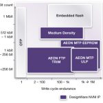
The DesignWare NVM IP port-folio above pictured shows that the “Medium Density” solution just announced by Synopsys should be the best fit if you search for NVM IP able to support MCU code, offering decent write cycle endurance (1K cycles or more) as well as code size up to 64 K-bit and still based on standard CMOS technology. Because this NVM family is based on a completely new architecture, the cell density is 5X better over lower bit count solutions. The Flash access time is less than 40 ns, well positioned to support low power MCU used in IoT for example. Automotive is also a target market for this NVM, so ECC has been added for reliability and the data retention is guaranteed for 10 years… at 125 C.
The high voltage circuitry (charge pump) and the memory array digital control is part of the IP, to ease designer life.
I have focused on MCU code application, in fact such Medium Density NVM IP target is mostly analog IC like:
- Smart sensors
- Power Management
- Touchscreen controllers
But the trend is to integrate microcontroller into Analog ICs, thus this NVM IP is expected to be massively used in the analog market segment. If you need to be convinced that NVM IP is a more cost effective solution, just take a look at the picture below: the curve is representing the IC area function of the bit count. When the IC is small and the flash complexity is very high (say above 256 kbits), embedded flash is better. But for most of the chips MTP is more cost effective (the largest part of the diagram area, on the left side).
More information about the new DesignWare® Medium Density Non-Volatile Memory (NVM) IP family.
From Eric Esteve from IPNEST