SILVACO 073125 Webinar 800x100

LRCX- Mediocre, flattish, long, U shaped bottom- No recovery in sight yet-2025?

LRCX- Mediocre, flattish, long, U shaped bottom- No recovery in sight yet-2025?
by Robert Maire on 04-29-2024 at 8:00 am

4d60ca863c5f696715ba448c97835bec

– Lam reports another flat quarter & guide- No recovery in sight yet
– Seems like no expectation of recovery until 2025- Mixed results
– DRAM good- NAND weak- Foundry/Logic mixed-Mature weakening
– Clearly disappointing to investors & stock hoping for a chip recovery

Another Flat Quarter & Guide

Lam’s report was uninspiring in that last quarter was $3.76B, the current quarter was $3.8B and guide is for $3.8B….flat, flat and more flat…the long flat bottom of a “U” shaped down cycle.

Revenue came in at $3.79B with EPS of $7.79 guidance is for $3.8B+-$300M and EPS of $7.50+- $0.75.

We are clearly bouncing along a more or less flat bottom of a normal semiconductor down cycle.

DRAM is better with HBM being the obvious bright spot. We would remind investors, again and agin , that HBM is only about 5% of the market, so even if its on fire its still not a lot.

Foundry/Logic is clearly mixed with more mature nodes slowing considerably.

NAND remains weak with hopes for a 2025 recovery as excess capacity gets used up.

China bumps up to 42% from 40%

China remains the biggest spender in the industry at 42% of Lam’s business versus only 6% for the US. China is outspending the US in Semiconductor equipment by a ratio of 7 to 1 (at least at Lam).

This remains a significant exposure for Lam and others if the US ever gets around to being serious about slowing China’s rapid progress in the semiconductor industry. At this point its likely way to late as China will have 5NM in the not too distant future thanks to US equipment companies enablement and the commerce departments lack of action.

Management is acting like no recovery in sight until maybe 2025

Management quoted on the call saying that things were setting up for a better 2025 which we think is code for “don’t expect a recovery anytime in 2024”.

Headcount was flat at 17,200 and if management felt a recovery was on the way we would expect an uptick rather than flat. Finally, management made comments about managing spend.

Overall, we did not get a positive tone from management on the call both in their comments as well as questions answered during Q&A. Overall a mediocre call at best and uninspiring.

ASML & Litho always precedes the rest of the industry

We would point out that litho orders always happen early in an up cycle given the long lead times. Deposition and etch tend to be more of a turns business with shorter lead times versus litho tools which can have lead times well over a year especially in EUV.

Thus its going to be impossible to see a recovery in Lam and AMAT until we get the prerequisite bounce in litho tool orders

Not a lot of new markets – Dry resist likely seeing “resistance”

Lam has not had huge success in breaking out of its traditional deposition and etch markets that it has been in since the Lam – Novellus merger in 2012.

Lam is trying to branch out into litho related markets by entering the dry resist market.

From what we have heard, this has been relatively slow going in large part due to cost/throughput issues. Rumors we have heard from customers point to a very high tool cost coupled with an ultra slow throughput winding up with a cost per wafer processed that rivals EUV costs or more.

In our view this will severely limit the ultimate market size as current spin on resist is dirt cheap by comparison and fine for the vast majority of applications.

Lam likely needs to find some other new markets either organically or through acquisition to get growth.

The Stocks

We have been saying for a while here that the semiconductor equipment stocks had gotten way ahead of themselves and the recent pullback seems to underscore our belief.

It should come as almost no surprise that Lam shares traded down in the after market as its clear that investors had been hoping for and pricing in a recovery that clearly isn’t coming any time soon.

Meanwhile we still have significant exposure to all the China sales.

Strength in HBM is a small percentage and doesn’t offset the broader weakness in NAND. The weakness in mature foundry/logic means that a key driver has run its course.

AI is obviously fantastic, but it too is a very small percentage of the overall chip market and only at the bleeding edge. TSMC has the lock on the leading edge AI market and we don’t see them running out and throwing money at equipment companies as we see quite the opposite in their more negative outlook.

Investors need to dissuade themselves of the inference that AI and HBM will be a boon to the chip industry. It will be great but the majority of the industry remains weak and in a funk that will take a while to recover from as this has been one of the deeper down cycles in our long experience.

We clearly expect some weakness out of Lam shares and don’t expect glowing reports from KLAC or AMAT and would expect weakness in their share price in sympathy.

Overall, we remain with our view that this is a long slow recovery hampered by macro issues as well as industry sp[ecific issues such as oversupply.

The CHIPS Act is also not coming to the rescue any time soon as you need to build the fabs before you buy the equipment so the trickle down from the CHIPS Act to the equipment makers is well over a year or two away.

Remain hunkered down……

About Semiconductor Advisors LLC

Semiconductor Advisors is an RIA (a Registered Investment Advisor),
specializing in technology companies with particular emphasis on semiconductor and semiconductor equipment companies. We have been covering the space longer and been involved with more transactions than any other financial professional in the space. We provide research, consulting and advisory services on strategic and financial matters to both industry participants as well as investors. We offer expert, intelligent, balanced research and advice. Our opinions are very direct and honest and offer an unbiased view as compared to other sources.

Also Read:

ASML- Soft revenues & Orders – But…China 49% – Memory Improving

ASML moving to U.S.- Nvidia to change name to AISi & acquire PSI Quantum

SPIE Let there be Light! High NA Kickoff! Samsung Slows? “Rapid” Decline?


WEBINAR: The Rise of the DPU

WEBINAR: The Rise of the DPU
by Don Dingee on 04-29-2024 at 6:00 am

why use DPUs

The server and enterprise network boundary has seen complexity explode in recent years. What used to be a simple TCP/IP offload task for network interface cards (NICs) is transforming into full-blown network acceleration using a data processing unit (DPU), able to make decisions based on traffic routes, message content, and network context. Parallel data path acceleration on hundreds of millions of packets at speeds reaching 400 Gbps is where Achronix is putting its high-performance FPGAs to work. Recently, Achronix hosted a LinkedIn Live event on “The Rise of the DPU,” bringing together four experienced server and networking industry veterans to discuss DPU trends and field audience questions on architectural concepts.

DPUs add efficient processing while retaining programmability

The event begins by recognizing that industry emphasis is shifting from smartNICs to DPUs. Ron Renwick, Director of Product Marketing at Achronix and host for the event describes the evolution leading to DPUs, where wire speeds increase, offload functionality grows, and ultimately, localized processor cores arrive in the high-speed data path. “Today’s model is the NIC pipeline and processors all embedded into a single FPGA,” he says, with a tightly coupled architecture programmable in a standard environment.

Renwick also notes that creating a dedicated SoC with similar benefits is possible. However, the cost to develop one chip – and its ability to withstand data path and processing requirement changes that inevitably appear as network features and threats evolve rapidly – make an Achronix FPGA on a DPU a better choice for most situations.

Baron Fung of the Dell’Oro Group agrees, noting that the hyperscale data centers are already moving decisively toward DPUs. His estimates pin market growth at a healthy 25% CAGR, headed for a $6B total in the next five years. Fung shares that hyperscalers using smartNICs still chew up as much as half their CPU cores on network overhead services like security, storage, and software-defined features. Moving to a DPU frees up most, if not all, of the server processing cores, so cloud and data center customers get the processing they’ve paid for.

Patrick Kennedy of the review site Serve the Home echoes this point, saying that smartNICs need a management CPU complex, while DPUs have processing, memory, storage, and possibly an operating system on board. Kennedy reminds everyone that introducing an OS on a DPU creates another point in a system for security management.

AI reshaping networks with DPUs in real-time

The wildcard in DPU adoption rates may be the fourth bubble in the image above – accelerated computing with AI. Scott Schweitzer, Director of DPU Product Planning at Achronix, says that in any networking application, reducing latency and increasing determinism go hand in hand with increased bandwidth. “Our high-performance 2D network-on-chip operating at 2 GHz allows us to define blocks dynamically on the chip to set up high-speed interconnect between various adapters in a chassis or rack,” he continues. Machine learning cores in an FPGA on the DPU can process those network configuration decisions locally.

Fung emphasizes that AI will help offload the control plane by function. “AI-based DPUs improve resource utilization of accelerated servers and in scalable clusters,” he adds. Using DPUs to connect and share resources may have a strong use case in large GPU-based AI training clusters, helping open the architecture around Ethernet.

Kennedy likes the idea of AI clusters, recognizing that training is a different problem than inference. “Once you have models trained, you now have to be able to serve a lot of users,” he observes. DPUs with Ethernet networks make sense as the user-facing offload that can help secure endpoints, ingest data, and configure the network for optimum performance.

Those are some highlights from the first half of the event. In the second half, the open discussion among the panelists uses audience questions to generate starting points for topics touching on future DPU features and use cases, hyperscaler and telecom adoption, coordinating DPUs with other network appliances, and more. Much of the value of these Achronix events is in these discussions, with unscripted observations from Achronix experts and their guests.

For the entire conversation, watch the recorded webinar:
LinkedIn Live: The Rise of the DPU

Also Read:

WEBINAR: FPGA-Accelerated AI Speech Recognition

Unveiling the Future of Conversational AI: Why You Must Attend This LinkedIn Live Webinar

Scaling LLMs with FPGA acceleration for generative AI


Podcast EP220: The Impact IQE’s Compound Semiconductors Are Having on the Industry with Dr. Rodney Pelzel

Podcast EP220: The Impact IQE’s Compound Semiconductors Are Having on the Industry with Dr. Rodney Pelzel
by Daniel Nenni on 04-26-2024 at 10:00 am

Dan is joined by Dr. Rodney Pelzel, he has over 20 years of experience in the semiconductor industry, with deep expertise in semiconductor materials engineering and the epitaxial growth of compound semiconductors. Dr. Pelzel joined IQE as a Production Engineer in 2000 and is now head of R&D and is tasked with creating unique materials solutions that enable IQE’s customers and provide them with a competitive edge. He is a Chartered Engineer and a Chartered Scientist, and a Fellow of the Institution of Chemical Engineers. Dr. Pelzel’s work has been widely published and he is the co-inventor of 30+ patents.

Rodney explains the significant impact compound semiconductors have on current and future products and the 30-year history that IQE has in this space as a global supplier. The application of Gallium Nitride (GaN) is explored in detail. Rodney explains the power and performance gains delivered by this technology and points to several large markets that can benefit from its capabilities.

He explores the growth of AI, both now and into the future and discusses how GaN can address a fundamental problem of power consumption for these new technologies.

The views, thoughts, and opinions expressed in these podcasts belong solely to the speaker, and not to the speaker’s employer, organization, committee or any other group or individual.


CEO Interview with Clay Johnson of CacheQ Systems

CEO Interview with Clay Johnson of CacheQ Systems
by Daniel Nenni on 04-26-2024 at 6:00 am

Clay Johnson CacheQ CEO

Clay Johnson has decades of executive experience in computing, FPGAs and development flows, including serving as vice president of the Xilinx (now AMD) Spartan Business Unit. He has a vision to enable the next phase of computing.

Tell us about CacheQ.
CacheQ is a little over six years old and we have about 10 people. We focus on application acceleration to simplify development of data center and edge-computing applications executing on processors, GPUs and FPGAs. Our QCC Acceleration Platform reduces development time and increases performance, enabling application developers to implement heterogeneous compute solutions leveraging processors, GPUs and FPGAs with limited hardware architecture knowledge.

My business partner and I envisioned CacheQ’s ideas and technology about 15 years ago. At that point, we recognized the need for performance beyond clock rate improvements in CPUs.

We continue to develop our software technology while engaging with customers to solve complex performance and technical challenges. Our customers have applications that may run single threaded on a CPU and need higher performance achieved by running multithreaded on a CPU. For higher performance, we can target accelerators like GPUs.

Tell us a little bit about yourself.
My career has been around technology, both in the semiconductor space and development platforms associated with complex semiconductor technology. I started off in EDA development tools, schematic capture and simulation. I worked for Xilinx (now AMD) for a long time. The last position I had was vice president of the Spartan business unit, a well-known product family from Xilinx at the time. I managed that along with the auto sector and the aerospace and defense sector. I left to run a company that developed a secure microprocessor with a high degree of encryption, decryption, anti-tamper technology and key management technology. We sold that company and I was involved in another security company. Then my business partner, who I’ve worked with for decades, and I started CacheQ.

What problems is CacheQ solving?
CacheQ accelerates application software. CacheQ targets a range of platforms from the absolute highest performance GPUs to embedded systems. Each platform has their own unique performance requirements. With embedded systems, we can target monolithic platforms comprised of CPUs and an accelerator fabric. An example of that is Jetson from Nvidia. In addition to performance, there is a requirement to reduce the complexity of application acceleration. Our development platform obfuscates the most complex steps to deliver application acceleration.

What application areas are your strongest?
Our customers deal with complex numerical problems in the medical, computational physics, video or large government entities. Essentially, high-technology companies with software developers implementing applications that solve complex numerical problems. Our target customers are software developers who traditionally write high-level languages like C or C++.

While it’s not a specific application or a specific vertical space, our tools are used for numerically intensive type of applications that require a lot of compute power to execute. Examples are molecular analysis and encryption and decryption. Computational fluid dynamics is a big area that’s used across a bunch of industries.

CacheQ has done various projects in weather simulation. Weather simulation can be traditional weather simulation or tsunami code that projects what will happen when a tsunami hits.

What keeps your customers up at night?
Driving performance is a daunting challenge because of the various technical challenges to overcome while trying to accelerate an application, especially those that are unanticipated.

Application acceleration can be compute bound or memory bound. At times it is unclear what target hardware to use –– is the target a CPU or a GPU? For some cases in performance, the target could be an FPGA. Another question is whether there are vendors that offer better development platforms and tools?

In many cases, the code written by an application developer runs single threaded and may need to be restructured to get higher performance to run in parallel. Attempting to accelerate an application includes plenty of unknowns. For example, we have code that runs faster on Intel processors. In other cases, it runs faster on AMD processors. It’s a multi-dimensional complex problem that’s not easy to solve.

What does the competitive landscape look like and how do you differentiate?
We are not aware of any company that does what we do. Our largest obstacle is customers who stay with the existing solutions. It’s a challenging problem. Customers are familiar with techniques used that put pragmas or directives into their code. An example is acceleration. Nvidia offers something called CUDA. CUDA is used to write code that runs in Nvidia GPUs.

It’s a complex tool chain to understand the software and how that applies to hardware. It takes time and energy to figure it out and where our competition lies. Getting over the hump of traditional software development and looking at new technology. Most developers have not been able to solve the problems that we solve. When we explain our technology and its complexity, they are skeptics.

Once we show developers our technology and demonstrate it, we typically hear, “Wow, you can do that.” It’s the existing mindset and existing platforms, as opposed to any competitor who’s doing exactly what we’re doing.

What new features/technology are you working on?
We continue to push our existing technology forward, which is further optimization to produce better results on target platforms. As new technology comes out, we update our technology to support those new technologies. We can always improve the results of what we deliver on the existing platforms we support. We continually look at target GPUs from AMD and Nvidia. With codes that come in from customers, we’re able to run them through our tools, look at them and analyze the results that we get and continually drive the performance that we deliver from various applications.

Beyond that, our technology supports heterogeneous computing, the ability to look at various technologies and split the task across these technologies. For example, most top-end acceleration is done with PCI-attached accelerator cards. Some code runs on the CPU and some on the GPU. We figure out what code needs to run where. It’s heterogeneous. At the same time, the world is looking at machine learning (ML). It is where everything is going and it’s dynamic.

Companies are investing significant amounts of capital to develop ML solutions across silicon systems, software frameworks like PyTorch, cloud services and platforms, new models, operational models, new languages. It’s broad and deep. We have technology to target multiple hardware platforms. We remove the need to code for specific platforms or vendors. I previously mentioned CUDA, the standard to get acceleration from ML models by executing on GPUs and why NVIDIA dominates.

CUDA is specific to Nvidia GPUs. Developers can’t run CUDA code on different GPUs. Coding in CUDA is challenging and, at the same time, writing CUDA code links into executing on an Nvidia GPU. Our technology removes the need to write ML libraries in CUDA. Developers write standard high-level languages like C or C++ and target CPUs and GPUs from both Nvidia and AMD.

Combining that with technology that allows access to low-cost cloud resources enables an environment that reduces model development time, delivers performance and low-cost access to high-performance GPUs. Anyone in the ML space knows the downside of GPUs today is cost. The most recent GPUs from Nvidia are $30,000. Many companies cannot afford or access that kind of technology in the cloud.

The direction we’re taking our technology for ML offers standard languages without vendor-specific code along with a development platform that allows developers access to low-cost GPUs. Customers tell us that’s a huge advantage.

What was the most exciting high point of 2023 for CacheQ?

Our customer engagements, our technology development and recognition of how our technology could enable ML are high points. We believe there’s a huge opportunity and challenge around ML development platforms.

Companies need much better software development platforms that could encompass not just a single vendor but multi-vendors. There are a significant number of models being developed and those models need to run across a variety of different hardware platforms.

No development platform offers what we bring to the market. 2023 was a year where we were engaging with customers and solving their complex problems. At the same time, we were working on our ML strategy. Our overall strategy really came together in 2023.

What was the biggest challenge CacheQ faced in 2023?
Traditional compute acceleration is not a growth area. Compute technology is being used for ML. The opportunity in 2023-2024 and beyond is various technologies around ML. Transitioning from a compute-focused company to include an ML offering was our biggest challenge in 2023.

How do customers normally engage with your company?
To learn more, visit the CacheQ Systems website at www.cacheq.com or email info@cacheq.com.

Also Read:

CEO Interview: Khaled Maalej, VSORA Founder and CEO

CEO Interview with Ninad Huilgol of Innergy Systems

CEO Interview: Ganesh Verma, Founder and Director of MoogleLabs


Alphawave Semi Bridges from Theory to Reality in Chiplet-Based AI

Alphawave Semi Bridges from Theory to Reality in Chiplet-Based AI
by Bernard Murphy on 04-25-2024 at 10:00 am

Alphawave Semi min

GenAI, the most talked-about manifestation of AI these days, imposes two tough constraints on a hardware platform. First, it demands massive memory to serve large language model with billions of parameters. Feasible in principle for a processor plus big DRAM off-chip and perhaps for some inference applications but too slow and power-hungry for fast datacenter training applications. Second, GenAI cores are physically big, already running to reticle limits. Control, memory management, IO, and other logic must often go somewhere else though still be tightly connected for low latency. The solution of course is an implementation based on chiplets connected through an interposer in a single package: one or more for the AI core, HBM memory stacks, control, and other logic perhaps on one or more additional chiplets. All nice in principle but how do even hyperscalers with deep pockets make this work in practice? Alphawave Semi has already proven a very practical solution as I learned from a Mohit Gupta (SVP and GM of Custom Silicon and IP at Alphawave Semi) presentation, delivered at the recent MemCon event in Silicon Valley.

Start with connectivity

This and the next section are intimately related, but I have to start somewhere. Silicon connectivity (and compute) is what Alphawave Semi does: PCIe, CXL, UCIe, Ethernet, HBM; complete IP subsystems with controllers and PHYs integrated into chiplets and custom silicon.

Memory performance is critical. Training first requires memory for parameters (weights, activations, etc.) but it also must provide pre-allocated working memory to handle transformer calculations. If you once took (and remember) a linear algebra course, a big chunk of these calculations is devoted to lots and lots of matrix/vector multiplications. Big matrices and vectors. Working space needed for intermediate storage is significant; I have seen estimates running over 100GB (the latest version of Nvidia Grace Hopper reportedly includes over 140GB). This data must also move very quickly between HBM memory and/or IOs and the AI engine. Alphawave Semi support better than an aggregated (HBM/PCIe/Ethernet) terabyte/second bandwidth. For the HBM interface they provide memory management subsystem with an HBM controller and PHY in the SoC communicating with the HBM controller sitting at the base of each HBM memory stack, ensuring not only protocol compliance but also interoperability between memory subsystem and memory stack controllers.

Connectivity between chiplets is managed through Alphawave UCIe IP (protocol and PHY), delivering 24Gbps per data lane. These have already been proven in 3nm silicon. A major application for this connectivity might well be connecting the AI accelerator to an Arm Neoverse compute subsystem (CSS) charged with managing the interface between the AI world (networks, ONNX and the like) to the datacenter world (PyTorch, containers, Kubernetes and so on). Which conveniently segues into the next topic, Alphawave Semi’s partnership with Arm in the Total Design program and how to build these chiplet-based systems in practice.

The Arm partnership and building chiplet-based devices

We already know that custom many-core servers are taking off among hyperscalers. It shouldn’t be too surprising then that in the fast-moving world of AI, custom AI accelerators are also taking off. If you want to differentiate on a world-beating AI core you need to surround it with compute, communications, and memory infrastructure to squeeze maximum advantage out of that core. This seems to be exactly what is happening at Google (Axion and the TPU series), Microsoft (Maia), AWS (Tranium), and others. Since I don’t know of any other technology that can serve this class of devices, I assume these are all chiplet-based.

By design these custom systems use the very latest packaging technologies. Some aspects of design look rather like SoC design based on proven reusable elements, except that now those elements are chiplets rather than IPs. We’ve already seen the beginnings of chiplet activity around Arm Neoverse CSS subsystems as a compute front-end to an AI accelerator. Alphawave Semi can also serve this option, together with memory and IO subsystem chiplets and HBM chiplets. All the hyperscaler must supply is the AI engine (and software stack including ONNX or similar runtime).

What about the UCIe interoperability problem I raised in an earlier blog? One way to mitigate this problem is to use the same UCIe IP throughout the system. Which Alphawave Semi can do because they offer custom silicon implementation capabilities to build these monsters, from design through fab, OSAT and delivering tested, packaged parts. And they have established relationships with EDA and IP vendors and foundry and OSAT partners, for example with TSMC on CoWoS and InFO_oS packaging.

The cherry on this cake is that Alphawave Semi is also a founding member with Arm on the Total Design program and can already boast multiple Arm-based SoCs in production. As proof, they already can claim a 5nm AI accelerator system with 4 accelerator die and 8 HBM3e stacks, a 3nm Neoverse-based system with 2 compute die and 4 HBM3e stacks, and a big AI accelerator chip with one reticle-size accelerator plus HBM3e/112G/PCIe Subsystem and 6 HBM3e stacks. Alphawave also offers custom silicon implementation for conventional (no-chiplet) SoCs.

Looks like Alphawave Semi is on the forefront of a new generation of semiconductor enterprises, serving high-performance AI infrastructure for systems teams who demand the very latest in IP, connectivity, and packaging technology (and are willing to spend whatever it takes). I have also noticed a few other semis also taking this path. Very interesting! If you want to learn more click HERE.

Also Read:

The Data Crisis is Unfolding – Are We Ready?

Accelerate AI Performance with 9G+ HBM3 System Solutions

Alphawave Semiconductor Powering Progress


Design Stage Verification Gives a Boost for IP Designers

Design Stage Verification Gives a Boost for IP Designers
by Mike Gianfagna on 04-25-2024 at 6:00 am

Design Stage Verification Gives a Boost for IP Designers

The concept of shift left is getting to be quite well-known. The strategy involves integrating various checks typically performed later in the design process into earlier stages. The main benefit is to catch and correct defects or errors at an earlier stage when it’s easier and faster to address. For complex SoC design, using this strategy can be the margin of victory. Siemens Digital Industries Software recently published a Technical Paper on deploying a shift left strategy for IP design. Called design stage verification, the paper provides an in-depth discussion on strategies and benefits for various IP design flows. The results can be dramatic. It’s a valuable document for anyone dependent on IP, which is just about everyone in chip design. A link is coming, but first let’s examine how design stage verification gives a boost for IP designers.

The Various IP Design Flows in Use Today

From a design perspective, there are basically three IP categories – hard, soft, and custom. Hard IP, such as cores and standard cells, are typically custom designs certified by a foundry at the time a process technology is defined. Soft IP typically consists of SRAM compiled from a library of pre-defined cells (bit cells, IO cells, etc.) to create the hard IP. And custom IP is typically created for a specific design, or to implement functionality that is patented or provides a competitive advantage. Traditional custom IP cell design requires manually creating a layout in a custom editor.

All of these methods require several forms of validation such as DRC and LVS to ensure the design is correct and compatible with the target foundry process. The Calibre family of products from Siemens is the industry leader in this area, so the technical paper naturally covers the most popular and trusted strategies for verification. The figures below summarize the traditional IP design verification flow and which Siemens tools are added to implement a shift left version.

Let’s examine some details about these flows and the benefits of shift left.

How Design Stage Verification Boosts the Process

A shift left methodology will enable design teams to enhance productivity and design quality while reducing time to market, as shown in the figure below. Note achieving these improvements requires coordination between design of low-level IP, macro blocks and the top-level SoC. A lot of moving parts and a lot of complexity to manage. 

Improved design time and quality

The Technical Paper does a great job explaining how to implement a shift-left methodology for the various IP design flows. I highly recommend you download it and get a first-hand look. To give you a sense of the scope of the document, here is a list of activities that are discussed in detail:

Targeted verification: The Calibre nmDRC Recon and nmLVS Recon tools provide automated ruleset selection that focuses on running rule checks for rules with local scope that target critical and systemic errors. By running these targeted checks during early design stages, designers can not only significantly reduce runtimes, but also generate results that are geometrically close to the source of the issue, reducing debug time as well.

On-demand DRC verification: The Calibre RealTime Digital and RealTime Custom tools are integrated with all major design and P&R tools. The Calibre RealTime tools provide immediate feedback for DRC violations in the design or implementation tool. This feedback enables designers to quickly analyze and correct DRC errors using Calibre signoff engines and rule decks, ensuring any fixes remain DRC-compliant.

Integration and runtime invocation: The Calibre Interactive interface supports the integration of Calibre tools into design and implementation environments and enables automated PV flows by providing user-friendly configurable interfaces for run set invocation, as well as automated pre- and post-run operations.

Debug integration and guidance: The Calibre RVE results viewer provides error debugging within all major design and implementation environments, enabling design engineers to work in a familiar design cockpit to debug and correct errors. Automated error categorization and filtering capabilities help designers perform targeted debugging in a systematic way by organizing results based on most likely root cause.

Automated waiver management: The Calibre Auto-Waivers® tool can be used in conjunction with the Calibre nmDRC Recon tool to define and maintain design rule waivers in collaboration with IP library providers and the foundries, all within a familiar PV environment.

Pattern matching: Symmetry in IP design is a core component of IP quality. The Calibre Pattern Matching tool simplifies complex design requirements through interactive pattern-enabled checking. Verifying transistor or even complex multi-layer device symmetry is a point- and-click check accessible directly in the layout design environment.

Reliability verification: The Calibre PERCTM reliability platform provides a powerful suite of electrical checks combined with the ability to apply context-aware checking that enable IP designers to find and eliminate reliability impacts such as electrostatic discharge (ESD) and latch-up during early design stages, reducing the time and resources needed to capture these issues in simulation.

Automated design layout optimization: Design for manufacturing (DFM) optimization consists of design adjustments that are not required, but that can improve a design’s manufacturability and/or performance and reliability. While DFM optimization traditionally occurs during signoff verification, the Calibre DesignEnhancer® tool offers three use models that enable designers to apply selected automated DFM optimizations during early design stages.

Advanced fill functionality: Calibre YieldEnhancer SmartFill and engineering change order (ECO) fill capabilities allow designers to maintain most of their timing analysis when an ECO occurs. Calibre YieldEnhancer programmable edge modification (PEM) uses layout analysis to move edges or polygons to optimize manufacturability.

Multi-patterning color assignment: Coloring assignment for multi-patterning is an important aspect in IP design because block/full chip designers must be able to color IP cells correctly in many various orientations and configurations.

To Learn More

This is just a summary of a lot of detail that is well-covered in this new Technical Paper from Siemens. You can download your copy of the complete document here and learn why design stage verification gives a boost for IP designers.


Intel High NA Adoption

Intel High NA Adoption
by Scotten Jones on 04-24-2024 at 6:00 pm

High NA EUV Final Pre Briefing Deck 4.15.24 embargoed til 4.18 at 7am PT (1) Page 07

On Friday April 12th Intel held a press briefing on their adoption of High NA EUV with Intel fellow and director of lithography Mark Phillips.

In 1976 Intel built Fab 4 in Oregon, the first Intel fab outside of California. With the introduction of 300mm Oregon became the only development site for Intel with large manufacturing, development, and pathfinding fabs all on one site.

Authors note, the Ronler Acres, Oregon site is home to RP1, research and path finding fab, and development fabs D1C, D1D, and three D1X modules with an additional module planned, and a rebuild of an old fab on the site also planned. Each of these development fabs or modules is similar in size to some other companies’ production fabs enabling Intel to develop a process and then ramp it into initial production in the same fab. The process is then copied out to “production” fabs.

Intel’s first EUV based process was i4 that entered manufacturing last year. i4 was developed in Oregon and then transferred to Fab 34 in Ireland for high volume production, the transfer to Fab 34 went “really well”.

The 18A process is in development now and High NA is being developed for the future 14A process. Figure 1 illustrates Intel’s process roadmap.

Figure 1. Intel Process Roadmap.

Over the history of the semiconductor industry there has been a continual drive to increase process density enabling more transistors in the same area. The first step in achieving more density is shrinking the lithographically printed features. Figure 2 illustrates the evolution of Exposure Systems and the resulting resolution.

Figure 2. Exposure System Evolution.

In the lower left of figure 2 we can see the formula for the resolution of an optical system (Rayleigh’s criteria).

  • CD is the critical dimensions, basically the smallest feature that can be resolved. Please note that the pitch achievable will be twice this number.
  • K1 is a process related factor that generally ranges between 0.75 and 0.25 and typically gets smaller as the process matures (smaller k1 equals smaller feature size).
  • λ is the wavelength of the exposing radiation. In the earliest exposure systems mercury arc lamps were used as a light source and G-line (436nm) and I-line (265nm) refer to peaks in the output spectrum of a mercury arc lamp. KrF (248nm) and ArF (193nm) refer to excimer lasers that combine Krypton (Kr) an inert gas and Fluorine (F) a reactive gas or Argon (Ar) an inert gas and F as a reactive gas in an excited state – in an excimer laser (excited dimer), these excited dimers decay giving off 248nm or 193nm light respectively. ArFi refers to ArF immersion (see NA below) and is also 193nm. EUV introduces a light source that uses a carbon dioxide laser to vaporize tin droplets producing 13.5nm light. As with k1 the smaller the wavelength the smaller the feature size that can be resolved.
  • NA is the numerical aperture of the optics, a measure of the acceptance angle of the lens. Higher NA gathers more of the reflections and therefore more information/higher resolution. Higher NA systems generally require more complex optics and for large diameter lenses it is particularly difficult. The maximum NA that can be achieved in air is 1.0 and ArF dry systems at 0.93NA are the highest achieved in exposure systems. ArFi (ArF immersion) refers to the use of ultrapure water between the lens and the wafer and this enabled 1.35NA for ArFi systems versus ArF dry systems where exposure is done in air. The higher the NA the smaller the feature that can be resolved.

High NA is expected to simplify the process flow, provide better yield and more flexible design rules.

The first High NA tool prototype is at the ASML factory. Intel got the second High NA tool in January 2024, see figure 3.

Figure 3. High NA System at Intel.

The system was shipped to Intel unintegrated and is being integrated only a few weeks behind the tool at ASML. The High NA tool (0.55NA versus 0.33NA for standard EUV tools) shares as many modules as possible with the 0.33NA tools, for example the laser source and wafer modules are the same as the new NXE:3800 0.33NA tool. The major development for the High NA tool is optics. There is a lot of data that the modules meet specifications and Intel as the first mover has a very close relationship with Zeiss (Zeiss builds the optics) and ASML. Mark said he is confident that the High NA tool will be available before there is too much multi-patterning required with 0.33NA tools.

Authors note, I asked if there was multi-patterning on the 18A process and he said there is some, not for resolution but for cutting to achieve tight tip-to-tip spacings.

Intel believes they are uniquely positioned to make the most of this tool with:

  • Power via.
  • Internal mask shop.
  • Directed Self Assembly for defect repair.
  • Using advanced illumination with advanced mask to push limits.
  • Pattern shaping with directional etch (possibly Applied Materials Sculpta tool?).

The first light for a High NA tool has been achieved at the ASML factory and first light at Intel will be “soon”. Development of the 14A process using High NA is planned for 2025, Intel is doing some work on the tool at ASML to get a jump on development.

One consideration with the High NA tool is size and having a Cleanroom that can accommodate it. Figure 4 illustrates the relative sizes of Deep UV, EUV (0.33NA) and High NA EUV systems.

Figure 4. System Sizes.

From figure 4 we can see that the original 0.33NA EUV systems are dramatically larger than DUV systems, in fact, cleanrooms must be designed to accommodate EUV systems. If you go into a Fab with EUV systems, they are easy to spot because there is a crane above the tool for maintenance work. Intel for example has a lot of older fabs that can’t accommodate an EUV system without major modifications to the building structure. High NA systems are ever bigger than 0.33NA EUV systems. Interestingly Intel’s Fab D1X and Fab 42 were both designed to accommodate 450mm equipment and therefore should be High NA tool capable. All Intel’s new fabs just completed or being built would presumably be High NA capable.

The current High NA tools are NXE:5000 development systems, the production High NA tool will be the NXE:5200 and Mark mentioned there would be at least three more generations of High NA tools after the NXE:5200. With 14A planned to be production ready two years after 18A, that would imply Intel will need to start receiving NXE:5200 systems in 2026 and 2027.

There is some discussion of Hyper NA tools possibly with a NA of 0.75. Mark mentioned that a lot of what ASML developed for the 0.55NA tool can be used for 0.75NA and that the tool will be the same size as the 0.55NA tool. The potential application for the 0.75NA tool would be for interconnect but the economics haven’t been proven yet.

Another aspect of High NA is the anamorphic design with 4x reduction in one direction and 8x in the other. When you take the current 6” reticle, account for edge exclusion with 8x reduction the die size is constrained and for some large die, stitching may be required and that requires consideration of where on the die to stitch. Intel is pushing for new 6” x 12” masks as a productivity improvement to enable large die without stitching.

It wasn’t discussed on the call, but one key question would be how much of a benefit High NA is over 0.33NA. My detailed simulations of High NA EUV single exposure versus LESLE double exposure with 0.33NA EUV, yield a just over 10% cost reduction, this is in addition to cycle time, yield, and design rule advantages.

ASML recently announced they shipped the third High NA EUV system to an undisclosed customer, although there are rumors it went to TSMC. Intel has been the most vocal company about adoption of High NA, but it is clear at least one competitor is at evaluating it close on Intel’s heels.

Scotten Jones is President of Semiconductor Manufacturing Economics and a Senior Fellow at TechInsights. Stay up to date with the latest from TechInsights by accessing the Platform for free today. Register or Sign-in here.

Also Read:

No! TSMC does not Make 90% of Advanced Silicon

ISS 2024 – Logic 2034 – Technology, Economics, and Sustainability

IEDM 2023 – Imec CFET


Electronics Turns Positive

Electronics Turns Positive
by Bill Jewell on 04-24-2024 at 4:00 pm

Semiconductor Intelligence 1

Unit shipments of both PCs and smartphones versus a year ago have turned positive. According to IDC, PC shipments in 1Q 2024 were up 1.5% from 1Q 2023, the first positive year-to-year change since 4Q 2021. Smartphone year-to-year growth turned positive in 4Q 2023 at 8.5%. The growth continued in 1Q 2024 at 7.8%. 4Q 2023 was the first positive year-to-year smartphone change since 2Q 2021. Despite the positive trend in 1Q 2024, IDC projects modest year 2024 growth of 2.4% for PCs and 2.8% for smartphones.

Electronics production for most key countries in Asia is on an upward trend. Taiwan electronics production was the strongest, with three-month-average versus a year ago (3/12) change in February 2024 at 19.7%, the strongest growth since November 2022. China electronics returned to double-digit 3/12 increases in January at 11.6% after declines in early 2023. March 3/12 growth was 13.3%. Vietnam electronics production 3/12 change increased 3.0% in March, the sixth consecutive positive month after eight months of declines. Japan and South Korea were the weakest countries. Japan had a 3/12 decline of 1.4% in January, the second consecutive monthly decline following 14 months of increases. South Korea electronics production 3/12 change decreased 4.2% in February after slightly positive growth in December 2023 and January 2024.

Electronics production in the United States and Europe was not as robust as in most of Asia. U.S. 3/12 change was 1.1% in February 2024. Growth has been in the 1.1% to 1.2% range for the last seven months, slowing from 4% to 8% growth in each month of 2022. The 27 countries of the European Union (EU 27) reported 3/12 change in electronics production of minus 7.2% in January, the seventh consecutive monthly decline. The United Kingdom (UK) 3/12 change turned positive at 0.8% in February after five months of declines.

The global economic outlook looks steady for 2024 and 2025 according to a recent forecast from the International Money Fund (IMF). IMF’s April projection has world GDP growth at 3.2% in both 2024 and 2025, the same rate as in 2023. Among the advanced economies, the U.S. is expected to show one of the strongest growth rates in 2024 at 2.7% before moderating to 1.9% in 2025. The Euro area and the UK are below one percent in 2024, accelerating to 1.5% in 2025. Among emerging and developing countries, China is forecast to have growth moderate from 5.2% in 2023 to 4.1% in 2025. Much of the growth in the emerging and developing economies will be driven by India with GDP increasing 6.8% in 2024 and 6.5% in 2025. The countries of the ASEAN-5 (Indonesia, Malaysia, the Philippines, Thailand, and Vietnam) are projected to have GDP growth accelerate from 4.1% in 2023 to 4.6% in 2025.

India is replacing China as the key economic growth driver in Asia. Based on IMF data, India was the world’s eleventh largest economy in 2013. India’s GDP grew at a 6.8% compound annual growth rate (CAGR) from 2013 to 2023 to become the fifth largest economy. If India’s growth continues at that rate, it could become the world’s third-largest economy by 2028, behind only the U.S. and China. A recent CNN article explored the drivers of India’s growth as well as its lingering problems with poverty.

While overall electronics growth in 2024 looks encouraging, there are signs of frailness. Although the key drivers of PCs and smartphones are back to growth, annual growth is expected to be low. Electronics production is increasing strongly in Taiwan and China. However, key countries such as South Korea, Japan, the U.S., UK and EU 27 are experiencing slow growth or declines.

Semiconductor Intelligence is a consulting firm providing market analysis, market insights and company analysis for anyone involved in the semiconductor industry – manufacturers, designers, foundries, suppliers, users or investors. Please contact me if you would like further information.

Bill Jewell
Semiconductor Intelligence, LLC
billjewell@sc-iq.com

Also Read:

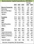
Semiconductor CapEx Down in 2024

Strong End to 2023 Drives Healthy 2024

CES 2024


2024 Outlook with Ben Packman of PQShield

2024 Outlook with Ben Packman of PQShield
by Daniel Nenni on 04-24-2024 at 10:00 am

Ben Packman PQShield

Ben Packman, Senior Vice President at PQShield, leads global expansion through sales and partner growth across multiple vertical markets, alongside taking a lead role in briefing both government and the supply chain on the quantum threat.

Tell us a little bit about yourself and your company.
PQShield is a post-quantum cryptography company creating the global standards and core technologies that will form the future security layer protecting the world’s leading organisations. Its quantum-secure cryptographic solutions work with companies’ legacy systems to protect sensitive data now and for years to come

As Senior Vice President, I am responsible for leading PQShield’s strategy and development. Our team is shaping the way our digital world is protected against the threats of tomorrow. In a time when quantum computers will soon be able to break current cryptography methods, we’re focused on empowering organisations, industries, and nations, with the ultimate quantum-resistant cryptography solutions.

What do you think the biggest growth area for 2024 will be, and why?
NIST’s post-quantum cryptography standards are due to be published within months, which will become the benchmark for cybersecurity globally. This will serve as a major growth area for PQShield as we expect to see a lot more companies taking the migration to post-quantum cryptography seriously.

We are able to guarantee to customers that our IP licensed products will be compliant with NIST standards giving them the confidence to incorporate our solutions into their post-quantum cryptography transition planning.

One area in particular where we expect to see growth is in the semiconductor and defence sectors, given their key position within the global supply chain and their need to secure highly sensitive data respectively.

How is your company’s work addressing this growth?
PQShield has already developed a mature suite of NIST compliant solutions across software, hardware and cloud applications and is already licensing its IP to strategic partners.

Several of PQShield’s customers that produce both software and hardware products are set to launch new solutions in 2024 that are already utilising PQShield IP. We have already partnered with industry leading semiconductor manufacturers like Microchip, AMD and Lattice, and world renowned defence contractors like MBDA and Collins Aerospace.

We’ve also focused on real-world implementation issues such as side channel and fault injection protection – we have our own lab in Oxford that we developed and verified working with Riscure and eShard. PQShield is leading the way in this area to ensure that our post-quantum cryptography solutions are robust.

What conferences will you be attending this year? 
We’ll be on the road a lot this year. We already have over 13 under our belt including Mobile World Congress Barcelona and OFC US. We’ve also had the pleasure of co-exhibiting with partners like AMD and Lattice at some of these events to showcase our products on the ground. 

Coming up we have IQT Europe, RSA Conference, The Economist Commercialising Quantum, HOST, CyberUK, FPGA Conference, RISC-V Summit, CHES and many others. By the end of the year we’ll have done around 50 events!

We are also very privileged to be co-hosting PQCrypto in our home in Oxford this year – gathering some of the brightest cryptographic minds from across the globe at the Oxford University Maths Institute, where PQShield began.

Additional questions or final comments?
Within a decade, the mathematical defences that currently keep online information safe will be at risk from a cryptographically relevant quantum computer, sufficiently powerful to break those defences. In fact, even before quantum technology exists, there’s a significant risk of ‘harvest-now-decrypt-later’ attacks, poised to extract stolen encrypted information when the technology to do so becomes available. We believe it’s critical that industries, organisations, governments, and manufacturers are aware of the threat, and follow the best roadmap to quantum resistance.

We are at a critical moment in this transition. With a recent wave of early legislation in the US, such as NSM-10 and HR.7535, as well as CNSA 2.0 and the National Cybersecurity Strategy, federal agencies and government departments are now mandated to prepare and budget for migration to full PQC by 2033. Simultaneously in Europe, cybersecurity organisations such as ANSSI (French Cybersecurity Agency) and BSI (German Federal Office for Information Security) have published key recommendations on the quantum security transition, and in the UK, the National Cyber Security Centre (NCSC) is recommending clear next steps in preparing for post-quantum cryptography. Internationally the awareness is growing among governments of the challenge ahead. We recently presented at the European Parliament, attended a roundtable discussion at the White House, and we’ve been key contributors to the World Economic Forum on regulation for the financial sector. 

When it comes to the security of tomorrow, the time to prepare is today, and at PQShield, we’re focused on shaping the way the digital world is protected from the inevitable quantum threat. 

Also Read:

Crypto modernization timeline starting to take shape

WEBINAR: Secure messaging in a post-quantum world

NIST Standardizes PQShield Algorithms for International Post-Quantum Cryptography


Real men have fabs!

Real men have fabs!
by admin on 04-24-2024 at 8:00 am

Semiconductor Ecosystem

“Real men have fabs” was an insult AMD founder Jerry Sanders hurled at his poor competitors who could not afford to build fabs. A few years later, AMD would be fabless, spinning off its manufacturing facilities as GlobalFoundries. This was the beginning of a transformative period for the industry.

Lisa Su could rightfully retort: “Real women don’t need fabs!”

Before the transformative era, all semiconductor companies were Integrated Device Manufacturers (IDM) that held the reins of designing, manufacturing, packaging, testing, and selling all their semiconductors.

Being a leader in all aspects of Semiconductor Manufacturing was becoming increasingly complex and expensive. Only a few companies had the market position and the financial strength to continue as IDMs.

The first elements to be outsourced were the backend manufacturing, the packaging and testing. It was labour-intensive and not a part of the manufacturing process that added significant economic value. First, operations were moved to Asia, and later, they were outsourced entirely as specialised companies started to appear. The Outsourced Assembly and Test (OSAT) market was born.

The IDM age was a boring time for market analysts.

The individual companies still did the front end (Wafer processing) of the Manufacturing.

In the late 1980s, the Taiwanese government offered Morris Chang, the founder of TSMC, a blank check to establish a local semiconductor industry. He had been working for Texas Instruments and observed that Japanese semiconductor factories outperformed US fabs significantly. The Japanese successfully transformed their society into a technology-based economy that would outcompete the US for over a decade.

Morris offered Intel and Texas Instruments to invest in the company, but they declined. Philips decided to trade their manufacturing technology and IP for a quarter stake in the new company, and the first foundry was born.

The increasing cost of building fabs and developing new technologies limited the number of new startups in the industry. However, new companies could enter the market with TSMC carrying the Capex cost of developing technologies and building factories. The fabless companies created a new market segment competing in design and let TSMC handle the manufacturing. In 2008, AMD gave up and became fabless themselves.

The current market structure

Since then, the Semiconductor market has become an even more complex web of submarkets and categories. This is happening as the industry has risen from an economic engine to become a matter of national security.

Understanding what happens in the semiconductor industry has never been more critical or challenging.

We continuously develop our industry model to analyse the industry and provide data and insights to our customers. This allows us to study the interfaces between the different submarkets of the value chain and detect market ripples early.

In a value chain, somebody’s future might be somebody else past.

We are not arguing that our model is correct or cannot be improved; we only know that it works for us now and that we must continue improving it.

A graphical representation of our industry model can be seen below:

The model has zones representing the different stages of the Semiconductor business. The design zone in the middle is where the design authority and absolute product ownership reside.

The manufacturing zone on the left represents front-end wafer manufacturing, and to the right is an assembly of systems by EMS or OEMs and the distribution channel, if applicable.

The brand zone is introduced as some semiconductor design owners also have a visible brand towards the end users of their products.

At the right are the end users of the Semiconductor products. We work with four different categories. The latest are large capital projects representing the large cloud and AI projects that have changed the dynamics of the industry lately.

The investment zone at the top represents what is needed to enable design and manufacturing. At the bottom, the supply zone represents the supply channels for front-end and back-end manufacturing.

We monitor the boundaries between these zones for insights that can enlighten us on what happens in the semiconductor market.

The major semiconductor business models

The industry’s most traditional business model is the integrated device manufacturer (IDM), responsible for both the design and manufacturing of the value chain.

Only the largest and most profitable companies have been able to maintain this business model due to the increasing costs of building wafer fabs. Memory companies also follow this model, as being competitive in memory is linked very closely to being competitive in manufacturing.

The rise of TSMC allowed semiconductor companies to go Fabless and outsource front-end manufacturing to foundries, concentrating on the design, sales, and marketing of semiconductor products.

A handful of companies use a mixed model, where they own their fabs and also use foundry. This Fab/Foundry model is popular amongst analogue and power companies that can operate analogue and power fabs, even though the leading edge digital manufacturing is outside their reach.

Some semiconductor customers with specialised demand are now so large that they design silicon for internal use. The Chip Designing Customers are mainly the large cloud and AI data centre-owning tech companies.

The last category is the Brand Customers. In this category, the semiconductor cannot be directly bought but is part of a system. The semiconductor inside is “branded” to the market as part of the system. Apple started this category, and the company promotes the semiconductor content of its products in its marketing. Recently, Nvidia also entered this category with its GPU-based AI systems.

There will be future categories as a result of two intertwined trends. The move from CPU to GPU requires a move from components to systems to work.

The owners of bricks

As the semiconductor sector has changed from an economically driven global industry to a politically influenced area of national security, the level of education on the market composition has deteriorated.

Because of the complexity of the industry, no good information is available about where the chips are physically made. Each chip has several countries of origin as it moves through the value chain.

Most chips are not made in Taiwan or by TSMC.

We base our research on the country of incorporation, where the political influence is most substantial and on financial Property, Plant and Equipment (PPE). Manufacturing capacity is not the same as that of PPE, but in the semiconductor industry, the most significant part of PPE is manufacturing.

Using this with our industry model, we get the following view of the distribution of PPE:

This gives a more nuanced image of what authority the properties are under rather than where they are located. This is increasingly important as governments are starting to lean on their local Semiconductor companies for patriotic investments.

In Q4-24, the most significant growth of PPE was in China, while Taiwan was declining. Europe also showed strong growth, which needs to be added to the political dialogue.

Applying our industry model gives the following output:

This is a different image than the broader press paints. From a PPE perspective, the two large IDMs with a foundry model (Intel and Samsung) dominate. The Foundry PPE is actually in decline while all other areas are growing.

The growth of the companies with mixed Fab/Foundry models is fascinating. This shows that the smaller mixed Fab/Foundry companies are adding PPE faster than the other models, a sign of them becoming more of a manufacturing company than a fabless company.

Traditionally, they have been unable to participate in the crazy manufacturing race of processing semiconductors, which they have outsourced. At the same time, these companies have manufactured analogue and power products on their fabs. While still expensive, these fabs don’t need the same insane technology as the processing parts.

The investment situation

As PPE depreciates quite fast in the Semiconductor industry, representing the rapid technological developments, the manufacturing part of the Semiconductor industry is dependent on high-octane Capital injections revealed in the cash flow statements under Capital Expenditure or Additions to PPE.

While fabless semiconductor companies can get away with a CapEx-to-revenue ratio (how much of revenue is spent on CapEx) of 3-4%, the IDMs need to shovel 28% of their income back into CapEx, as seen below.

This chart also reveals the manufacturing appetite of the mixed Fab/Foundry model companies. While Analog Devices and NXP are closer aligned with the Fabless model, Infineon and ST of Europe are pursuing more manufacturing. At the top is Texas Instruments, with a 29% Revenue to Capex Ratio in Q4-23.

TI’s recent Q1-24 result revealed that the company now has a ratio of 34%, showing a steadfast commitment to more manufacturing. The company also expect to be able to capture a $1B grant from the US Chips Act.

The Foundry investment situation

The “Most chips are made in Taiwan” story should be “Most Foundry manufacturing is in Taiwan” instead. In Q4-23, TSMC represented 62% of the revenue and 87% of the operating profits in the Foundry market, so it is undoubtedly the gold standard. (A deeper dive into the Foundry market is here.)

The CapEx to revenue ratio for the foundries can be seen below:

China foundries outspend all Others.

While the investments from the Taiwanese foundries have been high, they have been significantly outspent by the Chinese foundries. At times with CapEx that a higher than revenue, revealing the foundries operate in a different economical system than the reset. Recently also the American foundries have climbed higher and now has a CapEx to Revenue ratio slightly higher than Taiwan.

We keep monitoring the dynamics in the Semiconductor Industry using our proprietary models based on facts. If you want access to our data or neutral input to your strategy process, please contact us at: claus.aasholm@SemiBizIntel.com

Also Read:

Soitec Delivers the Foundation for Next-Generation Interconnects

Intel is Bringing AI Everywhere

No! TSMC does not Make 90% of Advanced Silicon