The annual SNUG (Synopsys Users Group) conference, now in its 35th year, once again brought together key stakeholders to showcase accomplishments, discuss challenges, and explore opportunities within the semiconductor and electronics industry. With approximately 2,500 attendees, SNUG 2025 served as a dynamic hub for collaboration and knowledge exchange.
This year, the conference was co-located with the inaugural Synopsys Executive Forum, an exclusive event featuring industry-impacting discussions attended by around 350 executives from Synopsys’ customer base, along with members of the media, analyst community, and investors. The forum facilitated in-depth discussions on the evolving silicon and systems landscape, the role of AI in the future of computing, and strategies to address key industry challenges.
The following summarizes the key insights gathered from various sessions at the event.
Synopsys CEO Sassine Ghazi’s Keynote: Re-Engineering Engineering
As semiconductor designs grow increasingly complex, traditional verification methods are proving insufficient. With quadrillions of cycles requiring validation, new verification paradigms have become critical. The cost and time associated with verification are too significant to rely on “good enough” approaches, making accurate and thorough validation indispensable.
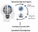
The integration of artificial intelligence (AI) is fundamentally reshaping electronic design automation (EDA) workflows, extending beyond mere efficiency improvements. As chip designs grow in complexity, new methodologies are necessary, and AI-driven workflows offer substantial productivity gains. AI adoption in EDA is evolving from assistance to full automation. Initially, AI acted as a copilot, aiding engineers, but it is now advancing toward specialized AI agents, multi-agent orchestration, and, eventually, autonomous design systems. Just as autonomous driving systems evolved in stages, AI in engineering must undergo a similar maturation process—gradually reducing human intervention while increasing efficiency.
Collaboration among industry leaders is crucial to advancing semiconductor innovation. Partnerships with companies such as NVIDIA, Microsoft, and Arm are essential for driving AI adoption in semiconductor design. No single company can tackle the growing complexity of semiconductor engineering alone, making collaboration key to accelerating innovation and developing solutions that keep pace with the industry’s rapid evolution.
Looking ahead, AI-driven “agent engineers” will work alongside human engineers—initially assisting them, but eventually making autonomous decisions in chip design. This shift will redefine the engineering process, unlocking new levels of efficiency and innovation while enabling more advanced and agile semiconductor development.
The impact of semiconductor advancements extends far beyond the industry itself, profoundly influencing how people live, work, and interact with technology—shaping the future of society. Synopsys’ mission is to empower innovators to drive human advancement.
A special highlight of the keynote session was the virtual guest appearance of Satya Nadella, CEO and Chairman of Microsoft. Nadella emphasized several AI milestones from a software perspective: the evolution from code completion to chat-based interactions, and now the emergence of Agentic AI, where AI agents autonomously execute high-level human instructions. This development has profound business implications, as discussed during the Fireside Chat session.
Fireside Chat: Sustainable Computing – Silicon to Systems
Synopsys CEO Sassine Ghazi and Arm CEO Rene Haas engaged in a thought-provoking discussion on sustainable computing and its implications for the future.
Emerging AI business models are beginning to disrupt traditional platforms and industries. AI-driven agents have the potential to automate user interactions, posing challenges for businesses and platforms that rely on conventional engagement and ad-based revenue models. As AI bypasses traditional interaction strategies, entire sectors could be reshaped. Companies that swiftly adapt to new AI technologies and business models will position themselves as industry leaders.
The Stargate initiative, a collaboration between OpenAI, SoftBank, Oracle, and Microsoft, aims to build massive data centers across the U.S. This effort presents challenges in energy consumption, thermodynamics, and infrastructure management. Large-scale AI projects will require innovative energy-efficient solutions, integrating renewable energy with cutting-edge computing infrastructure to meet their immense power demands. As AI workloads extend to edge devices, the development of low-power, high-performance chips will be critical to making AI viable in mobile and embedded systems.
In healthcare, AI-driven drug discovery has the potential to significantly accelerate the drug approval process—particularly in areas like cancer research—by improving success rates and eliminating costly early-stage trials.
Panel Discussion: Silicon to Systems Innovations for AI
A distinguished panel of experts from Astera Labs, TSMC, Broadcom, Arm, and Meta explored key innovations in AI-driven semiconductor development.
The discussion highlighted how AI is transforming chip design decision-making through advanced reasoning models that optimize design trade-offs and system performance. Panelists also examined strategies to reduce AI model training time, enabling faster deployment and iteration cycles.
Ensuring reliable connectivity in AI-powered devices was another key focus, as seamless data transmission is critical for AI-driven systems. Panelists emphasized the importance of designing products that align with customers’ development schedules while maintaining technological advancements.
Finally, they underscored the significance of strong IP partnerships, which foster collaboration and accelerate innovation across the semiconductor industry.
Panel Discussion: Re-Engineering Automotive Engineering
The complexities of integrating AI into automotive engineering were a central focus of this discussion, featuring experts from Ansys, Mercedes-Benz R&D North America, and Synopsys.
A key challenge in this domain is achieving seamless multi-domain interactions, where hardware, software, and AI technologies must function cohesively. Another critical factor is the high cost and complexity of data collection for advanced driver-assistance systems (ADAS), which is essential for training and validating AI-driven automotive solutions.
Mercedes-Benz R&D North America shared its approach to edge processing, where data is processed locally in vehicles rather than being stored or transmitted to the cloud—reducing latency and improving efficiency. The discussion also explored the role of synthetic data in training AI models. While synthetic data is widely used for validation, panelists noted that its effectiveness in training AI models remains limited. Additionally, electronic control units (ECUs) continue to evolve, playing an increasingly vital role in advancing autonomous driving capabilities.
The panel also addressed the rapid pace of product development in the automotive industry, particularly in China, where the minimum viable product (MVP) approach enables fast iterations but raises concerns about long-term reliability.
Panel Discussion: Custom High Bandwidth Memory (HBM) for AI
A panel featuring experts from AWS, SK hynix, Samsung, Marvell, and Synopsys explored this topic.
High Bandwidth Memory (HBM) has been a cornerstone of AI advancement, enabling high-speed data access with low latency, which is critical for AI workloads. In this discussion, panelists examined the role of HBM in AI and the ongoing debate between traditional HBM and custom HBM (cHBM) solutions.
While HBM offers benefits such as reducing I/O space by at least 25%, it comes at the cost of significantly higher power consumption. This tradeoff presents a challenge in balancing efficiency and performance.
Customization in memory solutions also poses scalability challenges. Memory vendors struggle with standardized production when customization is required, potentially hindering mass adoption. The lack of an agreed-upon architectural standard for custom HBM further complicates widespread deployment. However, future iterations of UCIe (Universal Chiplet Interconnect Express) are expected to bridge the gap between custom and traditional HBM solutions, promoting greater interoperability and scalability in AI hardware.
Panel Discussion: The Productivity Promise – AI Apps from RL to LLMs to Agents
This panel moderated by industry journalist Junko Yoshida and featuring experts from Nvidia, Microsoft, AMD, Intel, and Synopsys explored the broader implications of AI beyond chip design.
A key transformation in the industry is the shift from AI as a tool to AI as an autonomous problem solver, marking the emergence of Agentic workflows. In this new paradigm, AI no longer simply assists with tasks but takes on a proactive, autonomous role in solving complex problems.
As AI evolves, its impact on education becomes increasingly significant. Preparing the next generation of semiconductor engineers to collaborate with AI-driven design tools is essential, ensuring they can leverage these technologies in innovative ways.
AI’s learning capabilities are another major asset, enabling it to uncover insights and make connections that humans may not have initially considered—enhancing decision-making and innovation.
Additionally, the use of generator-checker models exemplifies a powerful approach in AI systems. In this model, AI agents act as both creators and validators, working in tandem to ensure reliability and accuracy, thereby advancing the trustworthiness and effectiveness of AI applications.
Panel Discussion: Realizing the Promise of Quantum Computing
A panel featuring experts from IBM Quantum, the University of Waterloo, Intel, Qolab, and Synopsys explored how quantum computing intersects with AI.
Quantum computing is still in its early stages, with significant progress made, but practical, large-scale systems may take decades to develop. While quantum mechanics is a broad phenomenon, its applications extend beyond quantum computers to various technological systems.
The relationship between quantum computing and AI is bidirectional, where Quantum for AI and AI for quantum both play vital roles in advancing each other. On one hand, quantum computing has the potential to significantly enhance AI by accelerating computations, enabling faster and more efficient model training. On the other hand, AI is being leveraged to optimize quantum systems, improving algorithms and error correction methods. However, building stable qubits remains a major challenge. Maintaining quantum states for computation is notoriously difficult due to their inherent sensitivity to external factors such as temperature and electromagnetic interference. Despite these challenges, the promise of quantum computing lies in its ability to handle complex problems beyond the capacity of classical computers.
To unlock high-value business applications, millions of qubits will be necessary, driving continued research and development to make quantum computing a practical and transformative tool for industries like AI, pharmaceuticals, and cryptography. A hybrid approach combining classical and quantum systems is necessary for practical quantum computing, leveraging existing infrastructure to control qubits. Effective system-level design, including hardware, software, and control systems, is crucial for making quantum systems functional.
Scalability remains a major challenge, requiring millions of qubits and error correction to achieve practical quantum computing, much like the scaling challenges faced by traditional semiconductors. The quality of qubits and the need for error correction are critical, as reliable qubits are essential for minimizing errors.
Manufacturability is key to scaling quantum systems, and the expertise of the semiconductor industry will help accelerate progress. Long-term investment and collaboration between the private and public sectors, as well as academic institutions and companies, were discussed as vital for advancing the field. Although quantum computing holds immense potential, practical applications will take time to develop, with ongoing experimentation driving innovation.
Revolutionary Results in Evolutionary Timescales
Toward the end of the Synopsys Executive Forum, I had an informal conversation with Aart de Geus, where he shared his insights on various topics, including sustainable power, renewable energy, CO2 emissions, his work with NGOs, and the role of nuclear power plants in future energy grids. This chat, which took place between sessions and was not part of the formal agenda, provided valuable perspectives on the broader implications of technological advancements and the rapid adoption of new technologies in the semiconductor industry.
Aart summed up the mission that drives both Synopsys and the entire semiconductor ecosystem, remarking that in the face of these critical challenges, the semiconductor industry is delivering “revolutionary results in evolutionary timescales.”
Summary
The Synopsys Executive Forum provided a comprehensive look at the future of AI, semiconductor engineering, and computing. The event sessions were thoughtful, organized, and productive, making the forum a top-notch experience. As the industry moves toward more autonomous AI systems, re-engineered automotive solutions, and scalable quantum computing, collaboration across the ecosystem will be critical in driving sustainable, high-impact innovation. Looking forward to more such events.
Also Read:
Evolution of Memory Test and Repair: From Silicon Design to AI-Driven Architectures
DVCon 2025: AI and the Future of Verification Take Center Stage
Synopsys Expands Hardware-Assisted Verification Portfolio to Address Growing Chip Complexity