webinar IPXACT banner

Synopsy Eats Their Own Dogfood

Synopsy Eats Their Own Dogfood
by Paul McLellan on 06-29-2015 at 7:00 am

One of the most interesting presentations that I went to was the last presentation at the Synopsys Custom Lunch (no, the lunch wasn’t custom, we all got the same, but the presentations were about custom design). Since the last presentation was by Synopsys themselves and not by a customer, it wouldn’t seem promising that it could be that interesting. But, as the saying goes, Synopsys “eats their own dogfood.” This is a phrase used in the software world (mostly) meaning that software companies use their own software.

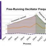
But in a sense the presentation was by a customer. It was by Anwar Awad who heads up the IP design group at Synopsys. They use exclusively Synopsys tools for all their IP design. Since they are #2 in IP overall (perhaps depending on how you count Rambus) and #1 in interface IP, they are not someone easily ignored. Although Anwar talked a lot about the difficulty of designing IP for FinFET processes, I want to focus on the bigger picture.

Bringing up a modern process node such as 14/16nm to volume manufacturing depends on several things. First, obviously, the process needs to be ready and the fab needs to have been built (well, duh). But that is table stakes. Without other requirements being satisfied, the fab will sit empty losing $50/second. To run wafers, the designs need to have been done. And to do the designs, the EDA flows need to be in place.

But also the IP. Some advanced groups such as Qualcomm develop almost all their own IP and use very little 3[SUP]rd[/SUP] party IP. But most groups are not in a position to do that, they get IP from the IP companies. Often ARM for microprocessors and Synopsys for interface IP. Design groups cannot tapeout their designs until they have access to the IP. So Synopsys is on the critical path to volume ramp in leading edge fabs.

This has broken the logjam that used to exist with regards to PDK availability. If foundries want timely IP from Synopsys then they need to provide the IP group with timely PDKs. Like those old Visa ads where stores “don’t take American Express” the Synopsys IP group “doesn’t take Virtuoso PDKs” because they only use their own tools.

One thing that Anwar emphasized was that timely PDKs doesn’t mean waiting until every last number is available in its final form. That is much too late to start development of IP if it is to be available in time. Synopsys starts IP development with version 0.1 of the PDK, knowing that it will go through many revisions before they will get final numbers. Of course this results in a lot of redesign but the alternative is to be late.

Synopsys have over 400 designers using their own tools for IP design, which in turns drives the tool development to delivering the factors necessary for success. IP design in FinFET processes is different from planar processes. So much of the silicon performance is dominated by layout parasitics that schematic simulation is largely irrelevant. Extracted layout is the only way to go. Of course this adds another wrinkle since now they have to do design with early DRC decks and adjust layout as the rules change.


Anwar showed the details of the IP development tool flow (above, click to get a version large enough to read) and you can see just how many Synopsys tools are involved.

Here are his other golden rules for success dealing with moving decks, models, flavors, and project starts:

  • Early LVS clean for extraction
  • Use larger-than-min design rules where possible to minimize changes
  • Leverage common blocks across IPs as much as possible – Single PLL team for example
  • Run density checking after device placement
  • Automation of running DRC with fill in place
  • Single design/layout environment independent of the foundry
  • Layout layers are common across all foundries to improve layout efficiency when moving from process to process


The diagram above shows the process for 16nm, showing when they started, when new projects were started and so on. This resulted in a lot of testchips for both the various flavors of TSMC and Samsung (which is also GF). The portfolio was USB2, USB3, DDR4, PCIe2, PCIe3, HDMI, DPHY, 10G KR, 16G.


Although a lot can be done in simulation, ultimately there is no substitute for looking at the “eye diagrams” from measurements of real silicon running at speed (see above). This is especially so for a new process with a new feature such as FinFETs, and especially early in the design cycle when everyone knows that the PDKs are not final, the design rules will change.

In total they ran over 30 test chips. Presumably most were on MPW shuttles but even so that is a major investment (I don’t know what the financial arrangements were but I doubt Synopsys paid retail).

Synopsys Custom Design page is here

Wikipedia page on eating your own dogfood (really) is here


The First Book on Smartphones!

The First Book on Smartphones!
by Daniel Nenni on 06-28-2015 at 8:00 pm

Now that we all have smartphones you may be interested in how this all came about. There are quite a few books about the smartphone technology and business but one of the first books that emerged after the iPhone era is by SemiWiki blogger and former EETimes Editor Majeed Ahmad:

Smartphone: Mobile Revolution at the Crossroads of Communications,
Computing and Consumer Electronics
.

In retrospect, the notion of a smartphone emerged in 1998 when Nokia, Motorola and Ericsson joined hands to turn the British computing platform Psion into a smartphone juggernaut called Symbian. However, the smartphone industry remained in doldrums until 2007 when Apple rewrote the mobile playbook with its iconic iPhone device.

What’s so special about this book? For a start, the book has it all—smartphone episodes about Nokia to Blackberry to Apple and Google. Next, it offers rich information on history, evolution, and technology and business development cycles of smartphones. It also has some very nice reviews from industry experts around the world:

Henning Wriedt, a veteran technology journalist, likes the book because it covers the era of the smartphone from A to Z. “I have something in my archive, which gives me a complete and detailed overview of an important part of this industry, spanned across nearly 20 years.”


A smartphone business archive for technology buffs

Then there is Lyle Appleyard, a computer programmer from Manitoba, Canada, who accidentally discovered this book on Goodreads. “I am not sure that I would have picked this book up if I had not won it on Goodreads. As a history buff and a bit of a geek, this book turned out to be right up my alley.”

When Appleyard began reading the book, he wondered if there was enough material about smartphone technology and business to justify a book with over 400 pages. He wrote after reading the book: “The author did a good job of gathering a ton of information for this book. It was intriguing to read about all the different companies that contributed to the development of the smartphone. Some I knew, some I had never heard of. It was interesting to read about the problems they had, the problems they caused and the possible future of the industry.”


The book provides a detailed treatment of Apple’s rivalry with Google

Sometimes technology books are a dry read which is not the case with this one. What is also unique about this book is that it turns a highly technical subject into an interesting read. “The author did a good job of explaining things,” Appleyard wrote. “It was very educational and shed some light on the smartphone and its history.”

The smartphone has been the key driver of semiconductor devices for nearly a decade. The book delves into both the hardware and software sides of the smartphone business. It narrates, for instance, how Steve Jobs gave the go-ahead for the iPhone project only when Apple engineers assured him that ARM-powered chips could handle the convergence of voice, data, music, and video.


The moment when mobile industry changed forever

The book also features a detailed treatment of ARM based chips and Intel’s Atom chips. Moreover, it provides an insider’s view of key players—such as Apple, Google, Nokia and Microsoft—and charts their respective journeys to smartphone riches. A sense of what worked and what didn’t could be highly valuable for managers working in companies that aim to explore opportunities in the smartphone realm.

Smartphone: Mobile Revolution at the Crossroads of Communications, Computing and Consumer Electronics is available in both paperback and e-book formats.


Is Interconnect Ready for the Post-mobile SoCs?

Is Interconnect Ready for the Post-mobile SoCs?
by Majeed Ahmad on 06-28-2015 at 2:00 pm

The interconnect technology is one of the unsung heroes of the system-on-chip (SoC) revolution. It’s the on-chip networking fabric that is used to link various IP cores on an SoC floorplan. The technology facilitates links between multiple processors, on-chip memories, hardware accelerators and more. In other words, interconnect is the skeleton and nervous system of an SoC device.

As chips get bigger to integrate more functions, they require more IP blocks, which in turn, demonstrates the increasing significance of a robust interconnect technology. Chipmakers have been building the interconnect part of the SoC internally through their internal bus groups; some of them still do that job in-house now. However, the increasing complexity of SoC devices has led to the emergence of specialized players like Arteris, the Campbell, California–based IP supplier who labels the SoC interconnect technology as network-on-chip (NoC).


Arteris calls interconnect the skeleton and nervous system of SoCs

The NoC interconnect technology of Arteris emulates packet transport networking technique for moving information inside an SoC device. Arteris appeared on the chip scene during the mid-2000s when IC vendors began to put the functionality of two to three chips onto a single large chip. Arteris got its first breakthrough when Texas Instruments morphed its interconnect IP into the OMAP4 application processor.

In 2006, Arteris shipped its first interconnect IP product, NoCSolution, which TI licensed for its OMAP SoC in 2007. Both OMPAP 4 and OMAP5 application processors have employed Arteris’ interconnect technology. TI’s OMAP4 chipset powered Motorola’s Droid smartphone while OMAP5 won SoC socket in the Amazon Kindle tablet.

In 2009, Arteris launched its second-generation NoC interconnect IP product—FlexNoC—that featured improved latency and made it easier for chipmakers to use the interconnect technology. Next year, in 2010, SoC powerhouses Qualcomm and Samsung licensed the flexNoC interconnect IP for their mobile chips.

Another high point for Arteris came in 2013 when Samsung used its FlexNoC technology in Exynos 5 Octa chipset which was shipped in the Galaxy 4 smartphones. Most of the world’s smartphones now use Arteris FlexNoC interconnect IP.

Fighting SoC Bottlenecks

The SoC coverage in the trade media is mostly centered on CPUs and GPUs because that’s cool stuff. But it’s crucial to have sophisticated interconnect design that can intelligently address quality-of-service (QoS) requirements for linking different IP building blocks on an SoC. For instance, cameras, CPUs and displays are sensitive about latencies. On the other hand, video codecs are bandwidth hungry.

The interconnect bottlenecks can result into problems such as routing congestion and timing closure. The repercussions of poor interconnect design also include the increase in die size and delay in time-to-market. Third, and probably the most important factor, is the rising cost of SoC designs.


Janac: It’s becoming hard for internal SoC teams to keep up with interconnect challenges

Arteris’ President and CEO Charles Janac points to the fact that the cost of building an interconnect was around $5 million back in the mid-2000s when the SoC movement took off at a larger scale. Now an in-house interconnect job requires an investment of $15 million to $20 million.

Janac adds that interconnect IP allows SoC designers to optimize latencies according to the requirements of the chip, and that can save chipmakers a lot of money. He claims that Arteris’ on-chip networking technology, which uses packetization and serialization techniques, can save SoC makers a couple of square millimeters in die size, 6 to 7 milliwatts of power, and nearly three months in time-to-market.

The interconnect technology is going to have a new set of challenges while SoCs are getting bigger and more power powerful to claim a stake in new market segments. For a start, the aggregate width and length of interconnect links inside an SoC will increase and that can lead to a routing congestion and timing closure déjà vu all over again.

SoC: The Next Frontiers

The specialized interconnect technology had its first major break in consumer-centric devices like mobile phones that began a relentless push for integrating more features at lower costs during the 2000s. The on-chip networking technologies like Arteris FlexNoS also helped mobile chipmakers address the constraints related to die area, power and time-to-market.

Fast forward to 2015 and new challenges are ready for the SoC interconnect fabric. First and foremost, there is a rapidly growing infrastructure for datacenters that will inevitably require more powerful SoC designs. Here, chipmakers are going to add more processor cores to boost energy throughput and thus reduce power consumption of datacenters.


Will interconnect evolve with larger chips and smaller nodes?

A new class of SoC designs will lead to a change in traffic patterns, and that can result in interconnect bottlenecks. Next up, there is the connected car juggernaut, where brand new audio, video and security applications will require a lot more processing horsepower to run intensive software algorithms.

The recent wave of mergers and acquisitions in the semiconductor industry is partly about the rising cost of SoC designs for smaller nodes like 14nm and 10nm. So far, popular SoC designs have ventured into high-volume markets like mobile phones to justify higher costs of complex SoC projects.

Now powerful SoC designs are opening up new avenues in markets such as connected wearables, Internet of Cars and datacenters that demand innovation before high volumes. Here, at this crossroads, interconnect technology, a crucial part of the SoC design, can play a vital role in steering SoCs clear of bottlenecks.

Also read:

Automate Timing Closure Using Interconnect IP, Physical Information

Arteris Flexes Networking Muscle in TI’s Multi-standard IoT Chip

Arteris Sees Computational Consolidation Amid ADAS Gold Rush


What’s New in Functional Verification Debug

What’s New in Functional Verification Debug
by Daniel Payne on 06-28-2015 at 7:00 am

We often think of EDA vendors competing with each other and using proprietary data formats to make it difficult for users to mix and match tools, or even create efficient flows of tools. At the recent DAC event in San Francisco I was pleasantly surprised to hear that two EDA vendors decided to cooperate instead of create incompatible formats in the area of functional verification debug.

Related – Are There Trojans in Your Silicon? You Don’t Know

VCD
The Value Change Dump file format has been around as a standard since 1995 as IEEE standard 1364-1995, and it works OK for smaller designs, yet as design size grows the VCD file can become multi-GB in size which really starts to slow down EDA tools in terms of loading, parsing and operating. EDA vendors then came up with proprietary extensions to VCD and other binary formats, but nothing universal has been widely accepted.

Cooperation
So the technologists at Cadence and Mentor Graphics decided to cooperate and create a successor to VCD so that modern SoCs with billions of transistors and massive waveforms can be functionally verified in the most efficient manner, saving users time. Ellie Burns from Mentor and Adam Sherer from Cadence presented at the Verification Academy booth at DAC. I first met Ellie at Viewlogic back in the 1990’s and have kept in touch over the years, and she also lives nearby in beautiful Oregon.

What these companies are proposing is a Debug Data API (DDA) to allow any EDA tool to create or view debug waveform data. Dennis Brophy of Mentor Graphics also wrote an informative blogabout DDA earlier this month. Here’s how the DDA works:

Cadence has validated this new DDA with their SST2 waveform format, and Mentor with their Visualizer. Some of the benefits of the DDA are:

  • VCD interoperability
  • Data portability
  • Openness

Adam Sherer blogged about how the DDA uses an open, Apache-licensed source code base so that each EDA vendor can optimize the interface implementation for their own tools.

Related – Getting the Best Dynamic Power Analysis Numbers

A demonstration showed simulation data created in the Mentor Questa simulator, then viewed with Cadence SimVision tool. Talking about Questa, I just learned that it has been updated to run up to 4X faster on regression tests, their new Visualizer Debug Environment sped up by 2-5X while taking less memory, running verification management coverage data collection is now up to 10X faster, and running the formal apps can be up to 8X quicker.

Cadence has committed to using this DDA approach with their newly announced Indago tool.

Related – SoC Debugging Just got a Speed Boost

Next Steps
If you’d like to get involved with the definition and use of DDA, the consider joining this group as they meet in the Valley on July 14th to review the specification.


Imec’s An Steegen Talks Future Process Technology

Imec’s An Steegen Talks Future Process Technology
by Paul McLellan on 06-27-2015 at 7:00 am

I’m an An Steegen groupie. Once or twice a year I see a presentation by her and it is a great summary in a ridiculously short period of time of all the potential upcoming semiconductor technologies. Yesterday was my annual fix at the imec Technology Forum (ITF). Today I got to sit down with her at the conference center.

An is different from most people at imec who, as a friend of mine described it, “are born at imec, do their PhD at imec and die there.” An went to the US and worked for IBM for over a decade in Fishkill, NY. She is now the SVP of process technology for imec. She is obviously not the only process technologist who know all this stuff. For sure every semiconductor company has their own experts. But she is the most free to talk about it. When did you last see TSMC or Intel giving details of all the work they are doing beyond 5nm?

Imec works with all the leading edge semiconductor IDMs and foundries including Intel, TSMC, GF, Samsung, SK Hynix, Micron, Toshiba, Sandisk. There are over 300 engineers assigned from these companies to work at imec. They all work together on programs. Imec is a sort of neutral ground, but it also allows for pre-competitive R&D cost-sharing and gives everyone access to their pilot line for novel technologies and equipment (which they may not even have access to in their own companies).

An sees part of their job as to see what technologies should be in the funnel for the future, then downselect it. Ultimately the semiconductor ecosystem has to make some decisions on what they will and will not do. The whole ecosystem needs to move since there is no good depending on a piece of equipment if nobody manufactures it, or on a material that is not available. For example, almost everyone decided on FinFETs after 20nm (or at it for Intel). Everyone has agreed not to worry about 450mm for the foreseeable future.

So I asked An what she saw as the most likely roadmap for the future.


First, push the fin as far as possible, higher and thinner fins. One big challenge, apart from the obvious fact that the higher and thinner the fin the more fragile it is, is to manage resistance and capacitance with very tall fins. Control of the process is also a big issue since everything is just a few atoms thick.

Next gate-all-round with lateral (parallel to the substrate) nanowires. Can relax the width a little versus fins.

Then stacking nanowires. The experience of vertical NAND flash and the techniques developed for doing that should help here too.

Next perhaps is vertical FETs. Unknown quite what the performance is. One nice feature of vertical FETs is that the gate-length can be varied just like in the olden days, by depositing thicker or thinner material. One big issue is how to connect to the bottom terminal of the gate.


Metrology is becoming a really big issue. All these vertical approaches also need the deposition to be conformal. There is also the possibility of local deposition which has new metrical needs.

The big challenge for the ecosystem is that we are still on a 2-year cycle but the roadmaps have to start really early so that everyone (equipment, manufacturers, materials, EDA, IP…) know what to get ready. This is especially acute with metrology who need to know where to focus.

EDA is no longer at arm’s length (nor is ARM, hoho) from the process stuff. Long gone are the days where SPICE parameters and design rules were all that were needed and the whole flow was up and running. Imec has something they call Design Technology Co-Optimization (DTCO) that focuses on this. For example, they worked closely with the EDA companies very early on double patterning which required huge changes to support all the coloring in everything from layout, place & route, verification, extraction and more.

A good example of what is required to move the ecosystem is spin devices. These are very very low power but slow. But so is a lot of IoT so maybe they are the perfect match. They are constructed in the backend in the metal stack. For sure active devices in the metal stack will break lots of EDA tools. I doubt you can even describe them in a PDK. But something like this clearly needs time to get ready. They can use the imec pilot line to fabricate the structures before, eventually, moving off to finalize details at each foundry.


Synopsys Vision on Custom Automation with FinFET

Synopsys Vision on Custom Automation with FinFET
by Pawan Fangaria on 06-26-2015 at 7:00 am

In an overwhelmingly digital world, there is a constant cry about the analog design process being slow, not automated, going at its own pace in the same old fashion, and so on. And, the analog world is not happy with the way it’s getting dragged into imperfect automation so it can be more like the digital world. True, the analog world loves perfection; do the process according to its needs and it’s happy. So, do we have an environment where we can accommodate the persistent demand from the analog world for preserving its unique identity and still deliver the required productivity improvement?

Since SpringSoft, a provider of custom layout tools, was acquired by Synopsysabout three years ago, I’ve wanted to find out what the digital giant has been doing to automate analog design. I found a great opportunity to talk to my long-time former colleagues Fred Sendig, Fellow at Synopsys and Dave Reed, Product Marketing Director at Synopsys. Fred is a well known technologist in the analog/mixed signal space that I worked closely with in my Cadence days. This meeting was an eye-opener to another level of innovation in the making from Synopsys, only this time, in the analog/custom design world. Instead of promising to fully automate analog design – something analog designers have long resisted — Synopsys’ vision is based on the concept of design assistance.

In the analog world, designer productivity counts more than anything else; automation can’t help if a designer has to redo the things to make the design perfect. Today, the custom design challenge has significantly increased with the introduction of FinFETs at lower nodes. Multi-patterning is required in the fabrication processes. The number of design rules and their complexities has increased significantly. The FinFET-based devices exhibit higher parasitic capacitances, and a higher resistance in local interconnect at lower-level metal layers. The device is more vulnerable to electro-migration due to extremely thin interconnect. Also, in FinFET designs, one device in the schematic can map to multiple FinFETs connected together in a complex series and/or parallel pattern to achieve desired design strength. So, the layout of even a simple circuit such as a differential pair may require the placement of hundreds of individual FinFET devices in complex matching patterns. It’s evident that automation is needed to counter such complexity and increased work, but how should it be done without violating designers’ intent and while keeping them happy?

Synopsys envisions preserving designers’ complete control over the layout and providing assisted automation to help increase productivity by 3X or more. The custom design environment envisioned by Synopsys will have several productivity boosters including:

  • Storing and reusing placement patterns and prior building blocks with further customization options
  • Using up-front knowledge of physical and electrical effects
  • Less effort required for creation and optimization, thus allowing designers to work at a higher level without losing their focus on the differentiating aspects of their design at the circuit and layout stages. In this way, the designs will be made perfect as early as possible in the design cycle to reduce the number of engineering change orders (ECOs).

The Synopsys vision for this custom design platform has circuit design and layout implementation flows working in a closed loop. The circuit design flow would let designers start from design entry and quickly converge on the final layout with a minimum number of ECOs. There would be fast extraction and simulation engines for quick analysis of electro-migration, IR drop, parasitics, etc. for the layout at different corners and its optimization for the best power, performance and area. There would be advanced analysis features to manage results from hundreds of corners.

The matching placement would keep the designer’s intent intact in the layout. The designer would then have the flexibility to modify it further according to her/his needs. The custom placer and router would perform automatic placement and routing of the devices. The electrical verification could be done during the layout. The physical simulation could be done at any stage before completion of the layout. This flexibility would deliver faster turn-around after any ECO in the layout.

Synopsysexpects to see ~3x productivity improvement in custom layout design with this approach compared to earlier solutions. Their IP design team has already been using this assisted custom automation flow at advanced process nodes. Synopsys’ MSIP team taped out several FinFET-based designs including USBs, DDRs, PCIe buses, HDMI, DPHY, and others at TSMC16FFP LL/GL and Samsung 14LPE and LPP.

Synopsys’ new custom design methodology is driven by the increasing challenges in FinFET technology at lower nodes and by customer demand for improved designer productivity. The solution is already in progress and there are several beta customers using it. It will be interesting to see this methodology rolled out. Assisted automation will be an important and effective upgrade for analog designs in the custom design space.

Pawan Kumar Fangaria
Founder & President at www.fangarias.com


Heard on the Street at ITF

Heard on the Street at ITF
by Paul McLellan on 06-25-2015 at 7:00 pm

As I said yesterday, I’m at the imec Technology Forum (ITF) in Brussels. So what have I learned from all the people that I’ve interacted with.

There were two press releases announced at a press conference yesterday. The first was that imec was expanding its relationship with Toshiba and Sandisk. This covers bringing EUV into volume manufacturing and other things. You may know that imec has major partnerships with the four biggest non-memory semiconductor manufacturers (Intel, TSMC, GlobalFoundries and Samsung) and with the four main memory manufacturers (Micron, SK Hynix, Toshiba/Sandisk and Samsung again). Toshiba/Sandisk had an existing relationship with imec but only for the memory aspect of the business. This announcement expands the relationship to cover non-memory processes.

As Dan already reported about the creation of a research company based in Chinese, with majority ownership from SMIC and minority ownership from Huawei, Qualcomm China and imec themselves. I was at the press conference where we asked questions of imec. Funnily enough it had the shortest embargo I have ever come across. It is 1.35pm and they tell us it is embargoed…until 2pm when the announcement was to go out in China. There was very little information other than what was in the press release. You probably know that China has committed billions of dollars to creating a domestic semiconductor industry with a 14nm process available by 2020. Of course there is more than just money to developing a 14nm process, just ask GlobalFoundries.

See UMC and SMIC 14nm Too Little Too Late?

We asked if the process was going to be FinFET. After a little discussion they were not allowed to say, although leakage would have to be a killer if it was just a vanilla planar process. We asked if export restrictions make it impossible to transfer a process from Samsung or someone else. Nobody knew. They just knew that they were in compliance with export regulations, hardly surprising.

I disagree with Dan that this is too little too late. China has made it a strategic imperative to have a growing proportion of domestic semiconductor content. If the development succeeds in creating a 14/16nm process that yields well, then it will be heavily used by Chinese companies even if by nobody else. Not just Huawei and Qualcomm, who are in the consortium, but also Lenovo, Xiaomi and more. If you look at the top 10 smartphone companies, it is lead by Apple and Samsung. But the rest of the list, apart from LG, is made up of Chinese companies some of which you have barely heard of. And it does matter, China is the largest smartphone market in the world, much bigger than the US, so the semiconductor content is important.

There is increasing distrust between China and US. For example, US carriers are either banned or “discouraged” from using Huawei kit since maybe the Chinese have trapdoors in them. Of course this is almost hilarious now we have discovered what the NSA has been doing, intercepting Cisco routers en route to their customers and compromising them. Do you think the Chinese would trust that mask data at GlobalFoundries in New York has not been compromised in some way by the security services? I doubt that US defense suppliers will be using SMIC as their foundry for similar reasons.

I learned a lot of doubts about EUV from talking to people at last nights dinner. But I covered them in yesterday’s post on EUV. The big issues being mask contamination under the pellicle, the non-availability of defect free masks (actually silicon molybdenum Bragg mirrors), and management of heat when you have a 250KW laser generating light of which under 10% is EUV of which under 10% reaches the photoresist. That’s a lot of waste heat to dump.

See also EUV: the View from imec

I met with An Steegen of imec today. Look for a blog about it at the weekend (or in the Monday newsletter if you are a newsletter type of person).

Did you wonder what Warren East was doing with his life-after-ARM? He was the CEO of ARM from 2001-13. Since then he has joined a number of board. One of those boards was Rolls-Royce. At the dinner at the end of the first day here, Simon Segars, the current CEO of ARM, told me that Warren will be the CEO of Rolls-Royce from July 1st. If you think of Rolls-Royce perhaps the first thing you think of are the luxury cars. But in fact that was sold to BMW. Rolls-Royce mainly makes jet engines for modern aircraft, in competition with GE and Pratt & Whitney. Quite a change from ARM.

The imec press release page, where both the press releases can be found, is here.


3 Design Hooks of Atmel MCUs for Connected Cars

3 Design Hooks of Atmel MCUs for Connected Cars
by Majeed Ahmad on 06-25-2015 at 7:00 am

In February 2015, BMW reported that it has patched the security flaw which could allow hackers to remotely unlock the doors of more than 2 million BMW, Mini and Rolls-Royce vehicles. Earlier, researchers at ADAC, a German motorist association, had demonstrated how they could intercept communications with BMW’s ConnectedDrive telematics service and unlock the doors.

BMW uses SIM card installed in the car to connect to a smartphone app over the Internet. Here, the ADAC researchers created a fake mobile network and tricked nearby cars into taking commands by reverse engineering the BMW’s telematics software.


Security is a big concern in connected cars

The BMW hacking episode was a rude awakening for the connected car movement. The fact that prominent features like advanced driver assistance systems (ADAS) are all about safety and security is also a testament is that secure connectivity will be a prime consideration for the Internet of cars.

Built-in Security

Atmel Corp. is confident that it can create secure connections for the vehicles by merging its security expertise with performance and low-power gains of ARM Cortex-M7 microcontrollers. The San Jose, California–based chip supplier claims to have launched industry’s first auto-qualified M7-based microcontrollers with Ethernet AVB and media LB peripherals. Atmel’s high-end MCU series for in-vehicle infotainment also offers the CAN 2.0 and CAN flexible data rate controller for higher bandwidth requirements.

Nicolas Schieli, Automotive MCU Marketing Director at Atmel, acknowledges that security is something new in the automotive environment that needs to be tackled as cars become more connected. “Anything can connect to the controller area network (CAN) data links.”


Atmel offers the ability to integrate cryptos in auto embedded designs

Schieli said that Cotex-M7 has embedded enhanced security features within its architecture and scalability. On top of that, he added, Atmel is using its years of expertise in Trusted Platform Modules and crypto memories to securely connect cars to the Internet. Schieli also mentioned the on-chip SHA and AES crypto engines in SAM E70/V70/V71 microcontrollers for encryption of data streams. “These built-in security features accelerate authentication of both firmware and applications.”

He explained how the access to the Flash, SRAM, core registers and internal peripherals is blocked to enable security. It’s done either through the SW-DP/JTAG-DP interface or the Fast Flash Programming Interface. The automotive-qualified SAM V70 and V71 microcontrollers support Ethernet AVB and Media LB standards, and they are targeted for in-vehicle infotainment connectivity, audio amplifiers, telematics and head control units companion devices.

Software Support

The second major advantage that Atmel boasts in the connected car environment is software expertise and an ecosystem to support infotainment applications. For instance, a complete automotive Ethernet Audio Video Bridging (AVB) stack is being ported to the SAM V71 microcontrollers.

Software support is a key leverage in highly fragmented markets like automotive electronics. Atmel’s software package encompasses peripheral drivers, open-source middleware and real-time operating system (RTOS) features. The middleware features include USB class drivers, Ethernet stacks, storage file systems and JPEG encoder and decoder.

Next, the company offers support for several RTOS platforms like RTX, embOS, Thread-X, FreeRTOS and NuttX. Atmel also facilitates the software porting of any proprietary or commercial RTOS and middleware. Moreover, the MCU supplier from San Jose features support for specific automotive software such as AUTOSAR and Ethernet AVB stacks.


Atmel claims its customers have built designs in a few weeks

Atmel supports IDEs such as IAR or ARM MDK and Atmel Studio and it provides a full-featured board that covers all MCU series, including E70, V70 and V71 devices. And a single board can cover all Atmel microcontrollers. Moreover, the MCU supplier provides Board Support Package for Xplained evaluation kit and easy porting to customer boards through board definition file (board.h).

Atmel is also packing more functionality and software features into its M7 microcontrollers. Take SAM V71 devices, for example, which have three software-selectable low-power modes: Sleep, Wait and Backup. In Sleep mode, the processor is stopped while all other functions can be kept running. In Wait mode, all clocks and functions are stopped but some peripherals can be configured to wake up the system based on predefined conditions.

In Backup mode, RTT, RTC and wake-up logic are running. Furthermore, the microcontroller can meet the most stringent key-off requirements while retaining 1Kbyte of SRAM and wake-up on CAN.

Transition from MPU to MCU

Cortex-M7 is pushing the microcontroller performance in the realm of microprocessors. MPUs, which boast memory management unit and can run operating systems like Linux, eventually lead to higher memory costs. “Automakers and systems integrators are increasingly challenged in getting performance point breakthrough because they are running out of Flash capacity,” said Atmel’s Schieli.

On the other hand, automotive OEMs are trying to squeeze costs in order to bring the connected car riches to non-luxury vehicles, and here M7 microcontrollers can help bring down costs and improve the simplification of car connectivity.


SAM V71 MCU lowers system cost by replacing MPU

The M7 microcontrollers enable automotive embedded systems without the requirement of a Linux head and can target applications with high performance while running RTOS or bare metal implementation. In other words, M7 opens up avenues for automotive OEMs if they want to make a transition from MPU to MCU for cost benefits.

However, the MPU and MCU worlds are constantly converging and colliding, and the difference between them is not a mere on-off switch. It’s more of a sliding bar. Atmel, having worked on both sides of the fence, can help hardware developers to manage that sliding bar well. “Atmel is using M7 architecture to help bridge the gap between microprocessors and high-end MCUs,” Schieli said.

Also read:

Atmel Tightens Automotive Focus with Three New Cortex-M7 MCUs

4 Reasons Why Atmel is Ready to Ride the IoT Wave

Atmel’s New Car MCU Tips an Imminent SoC Journey


Samsung: the Journey to 14nm and 10nm

Samsung: the Journey to 14nm and 10nm
by Paul McLellan on 06-24-2015 at 7:00 pm

At the Samsung theatre (cutely named the Samsung Open Collaboration (SoC) theater) I watched a presentation by KK Lin on using DFM to bring up their 14nm and 10nm processes. And yes, they are real. Here is a picture I took of a 14nm wafer and a 10nm wafer. Samsung announced that they would ramp 10n to volume production by the end of next year, 2016.


KK explained that Samsung uses DFM in two different ways (two “faucets” as the misprint on the slides has it). Design Enablement (DE) DFM is used to fix up design mask data. This is primarily optical proximity correction (OPC) and is used since 193nm light is being used with immersion lithograph (and double patterning for some layers) to print features much less than the wavelength. However, just doing that still leaves “hot” spots on the wafer where failure is more likely if the lithography and manufacturing is not absolutely perfect.


So another stage of DFM is Process Enablement (PE). Obviously a lot of process monitoring is done in a completely design independent ways using various process control monitors (PCMs). But that alone doesn’t get the yield ramp up fast enough for today’s consumer market places especially mobile. It used to be that a ramp to volume would take a couple of years, and now it is expected within a few months of final qualification. So the PE DFM is used to do design aware process monitoring and fault analysis. It is simply not possible to look at a whole wafer in any reasonable time at a resolution that can spot problems (“looking for a golf ball in California” is one way I’ve heard it described) so knowing where the hot spots and failures are most likely to be found makes it tractable.

KK’s conclusion:

  • Samsung Foundry provides comprehensive closed-loop DFM solutions at both design and process level
  • During design DFM signoff tools and flows are used to prevent failures
  • For process ramp, DFM is fed forward for defect monitoring, detection and estimation
  • Samsung Foundry 14/10nm DFM are synergized to serve customers’ collaborative yield learning. Not 100% sure what that means, maybe sounds better in Korean. But I think it means that by using DE and PE DFM they can ramp the leading customer designs to volume faster

Also on the Samsung booth was a nice demonstration of how much lower power FinFET is than planar. They had two smartphones running video. In one the application processor was 28nm HKMG, and in the other it was 14nm FinFET. If you look closely at the screens on the two phones, you can see that the one on the left has a temperature of 62°C and the one on the right 86°C.


They also had continuous displays showing the instantaneous power dissipations for the two phones. At the moment that I took the pictures, the 28nm chip was disippating almost 1.5W whereas the 14nm chip was 0.8W, close the half the amount of power.


A Closer Look at Fab Closures Around the World

A Closer Look at Fab Closures Around the World
by Pawan Fangaria on 06-24-2015 at 12:00 pm

Electronics is unusually an evergreen industry where companies make profit, yet end-product prices go down significantly after a brief period of price skimming. A product phases out quite fast (in case of smartphones every 1.5 to 2 years), but still yields big bucks for successful companies in its value-chain. How does this happen? How long it will continue to happen?

Well, the answer to the first question is highly capital intensive fabs with large wafer capacities and intelligent brains to invent newer ways of doing things with better YoR(Yield of Results), lesser CoR (Cost of Result), and lesser ToR (Time of Results). Of course, the worldwide demand lets it happen too. However, the demand does not sustain beyond a certain price-point; IoT (Internet of Things) market is a live example today, there is a tremendous latent demand, but at low price-point. The end result is – the price reduction has to continue, perhaps with reduction in OPM (Operating Profit Margin) of the companies. So, one can guess, the semiconductor business which started as a ‘blue ocean’ in the last century started turning ‘red’ due to couple of economic recessions and slowdown in this century. Several efforts are being made to keep the water ‘blue’, but how long will it remain blue and to what extent? Let’s analyze some data from an IC Insights’ report about fabs, published last week.

Between 2009 and 2014, just after the last global economic recession which started in 2008, 83 wafer fabs were either closed or repurposed. Majority of the fabs that were closed were 200mm and below wafer fabs. Arguably, the move was towards larger wafers to produce devices at lower cost. However, the economic stress is visible with the closure of some 300mm wafer fabs too in 2013.

This shows the need of consolidation in fab business. Although large mergers have happened in the past, or happening currently, more will happen going forward. New wafer fabs, and wafers at cutting edge technology nodes are no cheaper. The only way is to cut operational cost through consolidation. To me it appears to be a case of good business opportunity for large pure-play foundries like TSMC, GLOBALFOUNDRIES, UMC, and maybe Samsung foundry as well that can supply large wafers at reasonable cost, if not lower. Semiconductor designs should stay fabless.

A region wise graph of closed wafer fabs clearly shows how economies of different countries have affected the fab businesses in those regions.

Japan has closed most of the 83 fabs followed by USA and Europe. This exactly tallies with Japan, a leader in semiconductor business in 1990s, reduced to just one semiconductor company (Toshiba) in 2015 top10 list of semiconductor companies.

How will the electronics cost go down? Wafer cost is not expected to go down further. More mergers and consolidations are going to take place, and still a few 10nm and 7nm fabs will appear. If the fabs business gets consolidated at some pure-play foundry level, then the ocean may turn blue for fabs. However, the semiconductor equipment suppliers will bear the brunt because opening of new fabs will be limited. The electronics cost may stay where it is, if it does not go down further.

One thought comes to my mind is about new fabs in the regions where there are none existing; India is a live example. Should India still go for a new fab when there are fabs closing around the world? My opinion is, even if India opens a fab, it should go for the latest, not less than 300mm, may be 450mm so that it stays cost-effective and relevant for long term to recover the CAPEX and get enough ROI.

The IC Insights’ report is HERE.
Also read: Shift-West of Semicon Power Centers

Pawan Kumar Fangaria
Founder & President at www.fangarias.com