webinar IPXACT banner

Synopsys Buys Bluetooth IP

Synopsys Buys Bluetooth IP
by Paul McLellan on 07-22-2015 at 7:00 am

There is obviously a broad spectrum of semiconductor IP but broadly speaking it seems to fall into three buckets:

  • foundation IP: standard cells, memories
  • microprocessors and associated peripherals
  • interface IP

Foundation IP is where it all started. When I was at Compass Design Automation in the 1990s that was pretty much what we had: standard cells, gate-arrays, memory compilers. Artisan (which is now ARM’s physical IP division) started in that era. It was a hard sell since every semiconductor company had a group creating their own standard cells and so it was necessary to get higher than that in the company to sell successfully since the internal group wasn’t going to put itself out of business. We had better libraries since we had specialists designing them whereas it was an entry-level job in a semiconductor company and then people would move on to be back-filled with more new hires.

Microprocessor IP really started with ARM. Prior to that there was some second sourcing of microprocessors (for example at VLSI Technology we had the Hitachi H8). ARC now part of Synopsys, started inside an English video game company. Of course there are others. Much of the defensibility of microprocessor IP is not the silicon structures themselves but the associated tool chains and ecosystems which are much harder to replicate.

Then there is interface IP. Performance is usually defined by the standard for the interface, along with the specification, so it is hard to differentiate there. Either a piece of IP conforms to the standard or it is useless. So the differentiation here is all in the silicon. It is power and area, largely. Increasingly this sort of IP consists of two parts, a large digital block and the PHY, the actual interface to the outside world, to a cable, an optical transceiver or a radio. Synopsys has been building up this portfolio and it is, in fact, number one in interface IP. The internet of things (IoT) makes this even more important since every IoT device communicates with the outside by definition.

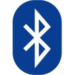
Last week Synopsys announced that they had acquired Bluetooth IP from Silicon Vision. Bluetooth is a short range radio interface originally developed by Ericsson in the early 1990s as a substitute for cables to headsets, keyboards, mice and so on. More recently the newer Bluetooth standards have improved power consumption and fixed some security weaknesses. It is now an IEEE standard (802.15.1). Bluetooth is named after the 10th century king of Denmark and Norway Harald Bluetooth (Harald Blåtand Gormsen in Danish). The bluetooth logo (see above) is actually a combination of the two Nordic runes for H and B.

As the Synopsys press release says:Silicon Vision’s highly integrated and ultra-low power Bluetooth Smart CMOS radio IP implements the Bluetooth 4.0, 4.1 and 4.2 low energy standards and includes an integrated on-chip transceiver matching network, which reduces the cost of external components and simplifies the board design. Silicon Vision’s Bluetooth Smart IP supports down to one-volt operation for extended battery life and includes a standalone encryption co-processor that supports FIPS-approved algorithms for highly secure connections. The Bluetooth Smart IP is silicon-proven at 180nm, 110nm, and 55nm.

The other area where Synopsys has been beefing up its portfolio is in the software security and quality market, with products to complement the Coverity acquisition from last year. On Monday, indeed, they finalized the acquisition of the Seeker product and R&D team from Quotium. The Seeker solution helps businesses find high-risk security weaknesses while fostering collaboration between development and security teams. It exposes vulnerable code and ties it directly to business impact and exploitation scenarios, providing a clear explanation of risks.

The Synopsys press release is here.


GPS Chronicle: The Beginning of the Commercial Era

GPS Chronicle: The Beginning of the Commercial Era
by Majeed Ahmad on 07-22-2015 at 4:00 am

Although primarily developed for military operations, this cutting-edge satellite technology was eventually allowed for civilian applications. The first interagency testing of GPS receivers was conducted in California in 1984. By July 1995, using Navstar constellation, GPS was fully operational across the country. Automotive navigation systems were among the early GPS products to become commercially available in the United States.

The former Soviet Union had developed its own GPS at the height of cold war—Global Navigation Satellite System (GLONASS)—as an answer to American Navstar. Both GPS and GLONASS were to be used by an increasing number of civilians, from aviators and sailors to car drivers. GLONASS signals were also used by a number of Western GPS receivers as a complement or back-up to GPS.


Navstar began serving civilian users in the 1990s

In the private sector, former NASA engineer Allen B. Salmasi founded Omninet in 1984 to track down truck fleets using military satellite systems. An Iranian émigré, Salmasi had spent the late 1970s and early 1980s working on satellite communications for NASA’s Jet Propulsion Laboratory.

After the U.S. government urged the agency to privatize part of the GPS technology, he used US$5 million of his family’s wealth to start Omninet, a satellite navigation system Salmasi marketed to companies eager to monitor the location of their trucks. After struggling for four years to expand, he merged his business with another small telecommunications startup to form a new venture that ultimately became Qualcomm.


Salmasi founded Omninet for fleet navigation

Garmin was another star of the commercial GPS pioneering era and was founded by Garry Burrell and Min Kao at a dinner in 1989. Both had worked for King Radio: a legendary manufacturer of aviation radios. In fact, Burrell had lured Kao, a native of Taiwan, to King Radio from defense contractor Magnavox, where Kao had been developing military navigation systems using the GPS. Now Kao took Burrell to Taipei to raise money for their new company. They were able to get hold of US$4 million, which also included their personal savings, though they didn’t have to rely on venture capital.

The duo eventually hired a dozen engineers and set up an office in Lenexa, Kansas, naming their new company as ProNav. The first product was GPS 100, a dashboard-mounted GPS receiver aimed at marine market that sold for about US$2,500. In 1991, a competitor named NavPro took the GPS pioneer to the court, and subsequently, its name was changed to Garmin, which was a combination of the two founders’ first names.


GPS 100: Garmin’s first dashboard GPS device

GPS was inherently designed by the U.S. Army as a military system and was still being used for that purpose. It had never been fully adapted for consumer uses. Although the U.S. government offered the infrastructure to the world, it didn’t allow equivalent level of service to business users. To protect military interests, Pentagon impaired signals released by the satellites in order to limit the accuracy of system for non-military use.

For national security reasons, the U.S. government had required that the signals be scrambled, making them accurate only to within about a hundred meters. Moreover, the operators provided no guarantee of service or liability cover, and if there was a political crisis, GPS could be switched off without any warning to its users. Another technical limitation of GPS was that transmission was sometimes unreliable.

Still, things still kept moving for the technology as GPS was incrementally advanced beyond the scope of a navigation tool that the U.S. military used. Then Pentagon vowed to stop impairing GPS signals within a year’s time; with that requirement no longer in place in May 2000, the devices became accurate within one meter, which in turn would help the technology take off in a variety of areas. With the end of “selective availability,” civilian users were able to pinpoint locations with at least ten times more accuracy.

The U.S. space agency also announced plans to maintain the satellite network at no cost for commercial users anywhere in the world. The location concept, once out of military playfields, began making new headways in customized location services. Applications were developed to make the effective use of technology in a number of niche areas where new pocket-sized devices promised enormous, untapped commercial potential.

Also read:

GPS Chronicle: The Early History

Content of this article is based on excerpts from the book Smartphone: Mobile Revolution at the Crossroads of Communications, Computing and Consumer Electronics.


SEMICON West 2015 Recap – Day 1 – Softening Markets, Sub 14nm and 3D NAND

SEMICON West 2015 Recap – Day 1 – Softening Markets, Sub 14nm and 3D NAND
by Scotten Jones on 07-21-2015 at 6:00 pm

Tuesday morning press briefing
The show started for me Tuesday morning with the SEMI press briefing. SEMI said there are 1,200 booths this year, 629 exhibiting companies and over 180 hours of programming. They also said pre-registration was up from last year and they expect 26,000 visitors.

Dan Tracy then gave an update on the markets.

Forecasts for the overall semiconductor market has been coming down as the year has progressed. Gartner just lowered their forecast to 2.2% and the average among forecasters is currently around 4%. The weakening euro and yen are holding down growth. The yen alone has accounted for a $600 million dollar reduction in semiconductor revenue year-to-date.

Silicon shipments year-to-date are up 8% versus growth last year of 11%. He thinks full year growth will be 5 to 6%.

Equipment billings are down 3.7% year-to-date but booking are up 3.7% so billing should rise later in the year. Memory is the big spender in 2015 and 2016 followed by foundry. Logic is generally flat for 2015 although some growth is expected in 2016. Overall the spending on equipment is expected to be $38, $40 and $42 billion dollars for 2014, 2015 and 2016 respectively. Foundries are ramping 200mm capacity in 2015 and 2016 driven by micro controllers, RF and power management.

Materials spending is expected to be $44, $46 and $48 billion dollars for 2014, 2015 and 2016 respectively.

Tuesday keynote panel on scaling the walls of sub-14nm manufacturing
The panel was moderated by Jo de Boeck of IMEC and included Mike Campbell of Qualcomm, Subhasish Mitra of Stanford University, Gary Patton of Global Foundries and Calvin Cheung of ASE.

Gary Patton (Global Foundries) was at IBM and with the Global Foundries (GF) acquisition has now moved into the CTO and head or R&D role at GF. He noted that he isn’t worried about physics but rather economics, he certainly seemed very confident and relaxed on the panel. He was bullish on GF’s new 22nm FDSOI process for IOT because it can be very power efficient running at 0.4 volts. Mobile is the big growth opportunity but is very cost sensitive. 10nm and 7nm will be more complex technologies, how to do that cost effectively is a big question. He thinks there are still orders of magnitude improvement opportunities, “we are still nowhere near where the human brain is”.

Mike Campbell (Qualcomm) noted that we need to look at end to end yield now including packaging and system yield. Sawing and packaging can change the IC performance. In the same vein he noted that foundries only want to provide PCM data but designers now need KLA data from the line. Silicon knowledge also needs to be transferred to packaging to help with yield ramps. “Semiconductors are a team sport now but everyone needs to speak the same language”. The tools all need the same data output without translators for greater interactivity. Tools for yield improvement need to be more predictive and interactive. In five years he wants 7nm technology with 28nm defect densities in high volume production. To get there we need to be more efficient.

Clavin Cheung (ASE) noted that die keep getting smaller while I/O is increasing and keeping it cost effective is a challenge. Yield needs to be monitored at each step though packaging. Mike Campbell interjected that there is no big yield company focused on packaging the way there is in the wafer fab.

Subhasich Mitra (Stamford) noted that development needs to take into account the entire system in order to optimize performance and power. A lot of bugs we see today are in power management functions embedded in the ICs. Bug fixes today are largely manual and take weeks or months, it needs to be automated and completed overnight. He thinks there is a 1000x energy efficiency opportunity still available.

I think to summarize the panel there is consensus that there is still a lot of room to produce more efficient – higher performance devices but it is getting harder and more collaboration is needed.

Tuesday afternoon TechSpot North Emerging Generation Memory Technology: Update on 3DNAND, MRAM and RRAM
Naga Chandrasekan of Micron provided Micron’s view of 3D NAND. Five years ago simple scaling ruled and there were many suppliers. Today there are few suppliers, many customers and simple scaling of 2D devices is no longer viable. Micron is focused 100% on 3D after the 16nm generation. Cost per Gb is lower for 3D than 2D. Scaling for 3D is limited by how high you can stack it and Micron thinks they can scale for at least 4 generations. There are a lot of process challenges around high aspect ratio deposition and etch, uniformity, hard mask materials, low temperature deposition, gap fill, stress and alignment. He thinks other emerging memories go into storage class memory but can’t displace NAND for storage because 3D NAND will still be the lowest cost.

Jim Handy of Objective Analysis noted that in the early nineties the switch from 1 or 4 bit DRAM to 8 or 16 bit DRAM stalled the introduction of new devices and again at 90nm DRAM stalled because nothing worked initially. He was skeptical that the introduction of 3D NAND would go smoothly.

Sanjeev Aggarwal of Everspin provided an update on MRAM. MRAM is a persistent RAM and combines the speed of RAM with non-volatility while providing better endurance than NAND. They view MRAM as high integrity non-volatile memory. The focus of Everspin engineering is on Spin Torque Transfer MRAM at 40nm and eventually 28nm to provide 1Gb + for PC applications. MRAM is manufactured in the top two metal layers of a CMOS process. 64Mb is currently in production on 90nm, it has 15ns access time with 10 year retention and better than 1E9 endurance. They are currently developing a 256Mb device – 40nm process on 300mm wafers at Global Foundries. They will then scale to 1Gb.

Robert Patti of Tezzaron gave an overview of the wide capabilities of Tezzaron. He thinks all processors will be 2.5D stacks in a few years. They take 28nm wafers from Global Foundries that are part way through the back end and fabricate things on top such as memory or MEMS. Tezzaron has a more than Moore fab to finish the processing.

From everything I have seen, I see 3D NAND as a huge hit over the next several years taking over from 2D NAND. For the other emerging memories they look like niche products to me.


See What’s Pushing up IoT Revenues

See What’s Pushing up IoT Revenues
by Pawan Fangaria on 07-21-2015 at 12:00 pm

The whole world’s eyes are at Internet of Things (IoT) market in various segments. The overall semiconductor ecosystem, starting from best suited technology nodes for IoT up to the final end products including sensors, microcontrollers, wireless chipsets, analog ICs, and so on are geared to avail the best opportunities from IoT market in coming years. If we put IoT in the perspective of connected cities or industrial applications, it doesn’t appear to be new, a significant amount of it is already happening in those segments. However, in modern age, IoT is being perceived as permeating in most of the aspects of our lives, thus unfolding the potential of internet in many more segments including home, automotive, wearable, medical, environment, and so on. The idea is for a human being to be able to monitor and control anything from anywhere at any time. So, definitely there will be many new segments evolving from the ground level adding into the expected ~25 billion IoT devices by 2020. We are already seeing good interest in home, automotive, and wearable segments; the wearable sales growth is showing promising future.

As we see in a graph from an IC Insights report, the connected cities has a large base with sales increasing at a modest rate, 19% in 2014 and forecasted 14.7% in 2015. The next is industrial internet at a base of about 1/4[SUP]th[/SUP] the base of connected cities and growing between 20 to 30% per year. The rest of the segments are relatively new and are miniscule in their base sizes. Look at the connected vehicle segment, it’s growing by 40+% per year but is expected to reach just $2 billion in 2015 which is ~3% of total forecast ($62.4 billion) of IoT market in 2015. Any guesses about how driverless cars can pan out in the near future?

The total IoT market does seem to grow at a healthy rate of ~29%, reaching $62.4 billion in 2015 from $48.4 billion in 2014. However, in my opinion, for this rate to sustain or grow further for the overall IoT market, the emerging segments that are with very small base need to grow their bases by multiple times. It’s encouraging to see the wearable segment; see its sales figure in 2014 and forecast in 2015. It’s more than 450% jump from $1.1 billion in 2014 to $6.1 billion in 2015. This will push wearable segment in 3[SUP]rd[/SUP] position in terms of base sales in the IoT market. Will this momentum in wearable segment continue? I guess it should because that comprises of many things including smartwatches, fitness bands, smart ornaments, smart glasses (Google is now working on smart lens), some healthcare devices, and so on. According to IC Insights earlier report, they anyway forecast IoT market to grow at a CAGR of ~21% until 2018 reaching ~$104 billion.

Whether we agree or not, we did see a budge in smartwatch segment after AppleWatch launch in April. According to Slice Intelligence, estimated Apple Watch sales could be about 3 million units by now. However there are conflicting rumours about Apple Watch sales in the market. Although the actual figure from Apple is yet to be seen, to me it appears to be much higher than Fitbit sales, the next major in wearable segment. Apple Watch is a compact good design but needs some key improvements. If Apple is able to address those in their next version of Apple Watch and that invades the large watch industry, then the wearable segment can grow by much larger extent.

The IC Insights report is HERE. See more details there on new connections to IoT which have grown from 282 million in 2013 to 410 million in 2014 and are expected to grow further to 574 million in 2015 and ~1.4 billion in 2018.

Also read: Apple Watch – A Great New Design, Needs More

Pawan Kumar Fangaria
Founder & President at www.fangarias.com


Starvision and SOS, a Perfect Match

Starvision and SOS, a Perfect Match
by Paul McLellan on 07-21-2015 at 7:00 am

SoC design these days is largely about assembling externally developed semiconductor IP with a small amount of differentiated content. Only companies who have to adopt new processes instantly develop a lot of their own IP. It makes more sense to license it. Partially because there is not a lot of differentiation in standards-based IP (they conform or they don’t) and partially because they can be very difficult to design. Not every design team could design a DDR4 PHY even if they decided it was a wise investment of time and money.

But bringing IP into a company is itself a challenge: by definition, nobody in the company understands the details since it was created by a third party. Even if that third party turns out to be part of the same company based in, say, India, it is only a marginal improvement over a true arms’ length relationship.

easy for engineers to find their way around it, start to make appropriate changes and so on. Of course saying IP almost makes it sound like it is a single file that is just dropped into the design but, of course, in reality it is thousands and perhaps tens of thousands of files: layout, netlist, Verilog, verification IP, scripts and more. Modern practice is to put the whole design into some sort of design data management system such as Cliosoft or Methodics.

One feature of Starvision is that it is extensible. EDA Direct, who are Concept Engineering’s US distributor, are also the distributor for Cliosoft’s SOS design data management system. Anis Weldon, one of the FAEs there, used the extensibility to integrate the two products so making importing IP, especially complex IP, much smoother.

For example, here an editor is being opened directly on an SOS repository, bringing up the netlist for a block directly in Starvision’s netlist viewer.


Another problem is that designers typically get the PDKs or Spice designs directly from the foundry and have no way to view them. The PDK viewer button can open the transistor level PDKs.


One area of complexity in IPs is that they often have multiple clock domains, possibly very large numbers of them. The clock tree analyzer button can instantly calculate the number of clock domains and show them in a graphical form.


The links are not all one way. Data such as the primitive and module count for each block are maintained for each version of the design that is checked in, and updated whenever there is a new checkin. This doesn’t just give the total number of primitives but keeps a separate total for each one.


The precise details of the functionality are not that important. It is the integration of Starvision with the underlying version control that makes for a powerful tool, and a lot less cumbersome than it would be to have to use the two tools separately, manually invoking whatever functionality is needed in one before switching to the other.

More information about StarVision Pro.

More information about ClioSoft SOS.

Also Read

Why Design Data Management: A View from CERN

ClioSoft Celebrates 2014 with 30% Revenue Growth!

Secret Sauce for Successful Mixed-signal SoCs


NetSpeed NoC IP or Architectural Synthesis Company?

NetSpeed NoC IP or Architectural Synthesis Company?
by Eric Esteve on 07-21-2015 at 12:00 am

When you look at NetSpeed’s NocStudio design tool, you first think “I see, NetSpeed is a new Network-on-Chip (NoC) IP company”. Are you wrong? Yes and no… No because NocStudio indeed generates a NoC. Yes, because the company objectives are going much farther than simply deliver a new NoC solution. According with Sundari Mitra, CEO and founder of NetSpeed, she has decided to launch this start-up to address an issue that architect and design teams are facing for decades, how to bridge the gap between architecture and Tape out? Sundari consider that NocStudio is “correct by construction”, addressing SoC synthesis. It’s a high level tool (higher than RTL synthesis), the idea is to bring the power of synthesis to SoC design. How does it work? Sundari answers this question: “This is an algorithmic solution to how SOC should be put together. It is all based on mathematics graph theory and networking algorithms to optimize what is done on a SOC. If you look at the tag line, it doesn’t say that we are a NOC company, it says we are redefining how SOCs should be designed.”

Before trying to understand NocStudio itself, it’s interesting to look at the background of NetSpeed technical team. At first Sundari: she has started working with Intel long time ago (on the nMOS 286) and since then has participated to dozens of SoC TO, facing last time issue like finding deadlocks, just before TO if you are lucky… and sometime after TO. Another point, Sundari was one of the founders of Prism Circuits, a start-up developing High Speed SerDes IP which has been acquired by MoSys in 2009 for $20M (the same price than Snowbush in 2007, but Prism Circuits was much younger).

Because NocStudio is based on the same type of algorithms than these used in Networking, one of the cofounders is a brilliant guy called Sailesh Kumar, who has worked in Cisco advanced research, Huawei, and comes from a strong networking background. It was clear from the beginning that NocStudio had to address cache coherent SoC designs and that’s the reason why Joe Rowland has join the team (Joe currently holds 80 patents on cache coherency and memory sub-system design).

The team has designed NocStudio as a graphical tool helping automate a SoC design using optimal-path algorithms adapted from computer networking and telecommunications. Architect will drop IP blocks into the left window and NocStudio will generates the links between the various IP as well as the script that defines the IP blocks for the synthesis compiler. NocStudio is not a place and route of floor-planning tool, but can be said as “floorplan aware”. To minimize interconnects between the various IP blocks, you need to know where these will be placed in the real SoC design. For architects who prefer working on scripts, the tool generates a script that you can edit and modify in a third window, synchronized with the graphic tool.

That’s great, but is NocStudio really efficient?

On the above figure we can see the chip optimization on a real life example, step by step: placement, layers, routing and channels optimization allows generating an optimized SoC. Not only the wire length and buffer count has been optimized, leading to a much easier place & route phase, but the final SoC is said dissipating 60% less power than with AMBA AXI interconnects.

So NocStudio is at first a front end optimization design tool and Sundari claims that such tools will become unavoidable for today’s SoC designs, like was software compiler and RTL synthesis before.

Sooner or later, the industry will embrace front-end design tools that inevitably will look very much like NocStudio. Architects who need a scalable, high-performance, correct-by-construction SoC interconnect should evaluate NetSpeed’s technology, especially if the design requires cache coherence.

From Eric Esteve from IPNEST


Apple Took All the Money

Apple Took All the Money
by Paul McLellan on 07-20-2015 at 4:00 pm

Apple has roughly 20% market share of the smartphone unit shipments. Android has pretty much all the rest with a tiny sliver for Microsoft Windows Phone, Blackberry, and Samsung’s Tizen. By any standard, Android is the highest volume operating system ever created. Famously, Microsoft makes more money on patent licenses for Android than it does building its own phones and mobile operating systems. Google gives it away but if manufacturers want the latest and greatest they have to keep Google as the default search. Google is a weird company in many ways, dabbling in a lot of businesses, but it actually really only makes serious money on advertising associated with search. People say it makes money on search, but even that is not really true (it makes a little licensing their search technology for internal use) it makes it on advertising. Which isn’t even a business model they invented themselves.

According to analyst company Cannacord Genuity, Apple made 92% of the operating profit in the smartphone industry in Q1 of this year 2015. In first quarter of 2014 that number was just 65%. Samsung, who are first in market share, took 15% of the industry profits. Once again it seems that Apple and Samsung together are taking more than 100% of the profit from the market and, while there may be exceptions, in aggregate everyone else is losing money. This analysis is, in fact, just for the top 8 smartphone makers but since it is almost a certainty that those even lower down the list are losing money then a full analysis would probably make Apple+Samsung an even bigger share of the overall market.


That covers a big range since there are low-end Android phones all the way up to the Samsung Galaxy 6 which pretty much matches iPhone feature for feature. Because it is an aspirational brand that is only at the high end, Apple doesn’t really compete in a direct sense with the low end suppliers like Xiaomi, Huawei and Lenovo. The high end Samsung Galaxies don’t either, of course, but Samsung has a big spread across the whole range and as it has for almost two years it has again announced that it expects a decline in profits in second quarter. Meanwhile the price of an iPhone on average is nearly four times the price of an Android phone.

I wrote last week about Gartner’s analysis of the Internet of Things (IoT) and how even with high volumes the profitability was likely to be low for the component suppliers and even the system-level hardware suppliers. The money would be made by the service providers and system integrators. It seems that reality is already here in smartphones too. Except for Apple with iOS. Since almost all the other suppliers run Android they cannot really differentiate much except on price. Low end smartphones are almost a commodity with very little brand-name loyalty. Xiaomi have been one of the superstars recently, coming out of nowhere three years ago to be #1 in the world’s largest market China. But even they have seen sales decline and are unlikely to make their target for the whole year.

See also SEMICON Day 1: IoT Everywhere…and China

In a few months, presumably, Apple with announce the iPhone 6S. Or probably at least two models like they did with the iPhone 6. Apparently Apple were surprised by how big the sales of the big screen iPhone 6 plus have been, which adds even more to profitability. Women like it since they keep it in their purse. Men prefer the smaller model since they keep it in their pocket. In Q4 and Q1 if history is a guide, Apple will be huge for Christmas and Chinese New Year. Then their volumes will fall off during the summer. If you are going to buy an iPhone, then August is not a good month to do it since the new models are probably imminent.


Choosing C++ or SystemC for High Level Synthesis

Choosing C++ or SystemC for High Level Synthesis
by Daniel Payne on 07-20-2015 at 12:00 pm

Most engineers learn by doing, and so at DAC in June an EDA vendor with High Level Synthesis (HLS) tools held a language tutorial on choosing C++ or SystemC for design and verification projects. The EDA company is Calypto, and Stuart Clubb put together the tutorial on using synthesizable C++ or SystemC. The design and verification flow for HLS starts with language entry, is followed by synthesis to RTL, and finally has verification that the RTL and entry language are equivalent:

Related – Verifying the RTL Coming out of a High-Level Synthesis Tool

The Catapult tool for HLS has been around for some 11 years now and engineers have done 1,000’s of tape-outs with it because this methodology generates high QoR for RTL in less time than hand-coding at the RTL level. Popular designs for HLS include video compression and decompression, image processing, and wireless or wireline applications. Big-name companies have been using HLS tools like Catapult for multi-million gate hardware projects:

  • NVidia – Tegra X1
  • Qualcomm – Snapdragon
  • Google – VP9
  • ST Micro – Monaco and Cannes
  • CPqD – 400Gb Coherent Optical Processor

Related – NVIDIA and Qualcomm Talk about High Level Synthesis, Samsung on Low Power for Mobile

C++
This language is like most modern programming languages in that it is very abstract and doesn’t including IC details like timing with clocks and resets, those lower-level details are added by the HLS tool itself. You can use bit accurate data types in C++ to model your hardware ideas, and the interfacing is abstract.

SystemC
With SystemC you get a set of C++ classes and macros that are useful for HLS because you can define clocks and resets. Hierarchical modules can be used along with concurrent processes (aka threads). Interfaces can be explicitly defined for more control.

Which Language?
Here’s a chart showing a range of interfaces versus functionality and how these two HLS languages are mapped out along with RTL coding:

Related – Shorten the Learning Curve for High Level Synthesis

Both languages offer bit accurate data types, so take a look at a comparison example using a Variable Rate Polyphase Decimator where our code has configurable taps and phases, plus configurable data types and widths:

This design is quite compact to code in synthesizable C++:

The same design coded in SystemC adds a modular I/O to abstract synchronized data transfer, and the untimed filter code is placed in a thread:


When synthesizing this design into RTL code the designer gets to choose the target technology, clock frequency, resource mapping, and the trade-offs between Unrolling, pipelining area and latency.

Related – HLS – Major Improvement through Generations

Running functional simulation on the C++ code is the fastest, followed by SystemC as second fastest, while RTL simulation is always the slowest.

When coding in C++ there are no interface details on the function call, so HLS maps function arguments to a library of interface protocols. With SystemC you can write pin-wiggling and transaction style views of interfaces, so more control is provided.

For hierarchy in C++ each function can have on clock only and then synthesis creates channels between each function. Hierarchy in SystemC is a full RTL-style instantiation and wire connectivity to any depth, just like with Verilog or VHDL.

Verification
A big benefit of using C++ or SystemC for verification is that your simulation times are much shorter than with RTL code. Adding formal technologies to your verification flow makes sense because it adds C property checking, enables formal verification of RTL netlist against your source code, and you can continue to use your RTL LEC (Logical Equivalency Checking) for RTL to gate comparisons.

Summary
A quick table neatly summarizes some of the comparisons between using C++ or SystemC languages:

C++ offers the fastest simulation times and is about 20X to 200X faster than SystemC, and is well suited for complex feed-forward algorithm designs, while being limited to pre-built interface libraries.

SystemC is still much faster at simulating than RTL code, and you can write everything that you can in C++ by using the Modular I/O and hierarchy, and it unifies RTL-level and higher abstraction language by offering hardware-centric constructs.

Fortunately with the Catapult tool you can use both languages and both sets of data types natively. Maybe it’s time that you considering trying an HLS flow on your next SoC design.


Antun Domic, on Synopsys’ Secret Sauce in Design

Antun Domic, on Synopsys’ Secret Sauce in Design
by Paul McLellan on 07-20-2015 at 7:00 am

Antun Domic is the GM of the Design Group at Synopsys. I sat down with him a couple of weeks ago.

His name is Croatian although, of course, there was no Croatia back then it was part of Yugoslavia. But in fact he grew up in Chile and went to university there where he studied EE and math. He came to the US as a grad student and did a PhD at MIT in math. He returned to Chile in the Pinochet era and taught for 2 years before returning once and for all to the US (his wife is American). He worked briefly for Honeywell in EDA.

He then went to MIT Lincoln Labs doing work funded by DARPA on restructurable wafer-scale VLSI, big systems larger than chip, essentially silicon compilation. He says DARPA was key in the mid to late 1980s funding EDA research at MIT, Berkely, CMU etc and is probably one key reason why even today EDA is dominated by US companies.

He then moved to the microprocessor group of Digital in the era when every company had internal CAD. I actually interviewed there with his predecessor Alan Hanover, who went on to found Viewlogic. Now part of Synopsys! He left after tapeout of the second Alpha chip and went to Cadence.

At Cadence he ran the group that was doing their synthesis product back then called Synergy. But Synergy had a hard time against Synopsys’ Design Compiler and was eventually canceled (and Cadence bought Ambit where I was VP engineering, but that’s my story not Antun’s). Antun became head of P&R, where Cadence was a lot stronger.

He came to Synopsys in 1997, so nearly 20 years ago, and ran logic synthesis and timing analysis (DC and PrimeTime). Now he has essentially all design tools: logic synthesis, timing, P&R, test, layout verification, circuit simulation and custom layout.

The design environment has changed a lot. 15 years ago everyone designed on node N (whether analog or digital) and was just waiting to move to node N+1. Today there is a much wider spectrum of designs. 90nm for automotive. 28nm will be around for a long time. Obviously lots of stuff on 14/16nm.

A big business imperative for Synopsys is to service 10nm with their leading edge customers (the usual suspects but I won’t mention them since they sometimes get upset about that sort of thing). However, an important part of the industry will remain on established nodes. Some design is still done by hand but most is automated with the usual Verilog, DC, STA, P&R flow. One of the great successes of EDA is the level of automation which is stunning. Today we can do flat P&R of 10M cells, with 10 corners, GHz clocks, FinFET. Design Compiler in the early 1990s was limited to 5K gates.

The focus recently has been introducing ICC2 (Synopsys’ place & route system, called Newton internally). One of the rare occasions that an EDA company looks at the problem completely from scratch: new database, new optimization, new clock-tree synthesis. The only parts kept were placement and routing (which is under 25% of the code).

The main reason for starting from scratch was that you couldn’t just depend on getting increased single thread performance, just more cores. So almost everything needed to be rewritten for threading. Also, existing algorithms don’t always parallelize effectively and so new algorithms are needed to do that. On the horizon was 20/16/14/10 which would need much more speed and data capacity. ICC1 was already the fastest tool available but was still too slow. The plan was for a 5X increase in raw speed. For design planning it ended up 10X faster. There was 5M lines of new code written. Most of the Magma engineering team was retained (despite Magma’s P&R product Talus being phased out) and they contributed to this effort. Other additions were in timing analysis and circuit simulation, for example the current head of PrimeTime was the head of timing analysis at Magma.

Another major project was to take Custom Designer (Synopsys’ internally developed custom design) and Springsoft Laker (acquired, largely confined to Asia). An important project to combine the two technologies has been ongoing. Watch this space for official announcement.

Physical verification, called ICValidator is a much larger business than most people realize. It is used heavily internally in IP development and QA and is now much better supported by foundries. It has been used used to support the largest FinFET designs for many foundries.

The flows have changed. P&R is the tool where a lot of technologies get done today (metal fill, power minimization, chip finishing) and so connecting layout, extraction, verification is very important, such as running DRC/LVS without leaving the P&R environment. Incremental analysis is a big time saver: don’t reextract the whole chip if only a few nets have changed. Synopsys has a big effort in incremental analysis.

Things are much better. 10 years ago there were lots of data transfer format flow issues. Eventually stuff got truly standardized: .lib (aka liberty), LEF/DEF, UPF. Effort now is to make flows incremental and deciding when to do analysis.

Another challenge is teaching algorithms when to give up. When synthesis or P&R can’t make the constraints. Placement has to keep improving too since it is still handling a sea of standard cells but now IP is not just a memory in the corner but perhaps 500-1000 larger blocks spread through the sea. So the cells are no longer “roughly” the same size as with pure standard cells.

His group has about 2000 people distributed everywhere. Even, to his amazement, 70 engineers in his home country Chile.

See also Bijan Kiani Talks Synopsys Custom Layout and More


Cost Modeling as a Decision Making Tool

Cost Modeling as a Decision Making Tool
by Scotten Jones on 07-19-2015 at 10:00 am

The use of simulation is well established in the semiconductor industry. Virtually all circuit designs are run through a Spice simulation, layouts are analyzed for timing issues and even process development employs process simulation tools. What I believe is less widely used but just as useful is cost modeling.

The semiconductor industry has been driven by Moore’s Law for the last fifty years. Moore’s Law is not just about increasing chip density but also about lowering costs. Cost modeling can be a very useful tool in the process development, design and procurement phases of a chips lifetime allowing various alternatives to be evaluated for cost impact and even in supplier negotiations.

The first project I did after founding IC Knowledge was to evaluate potential cost savings for a customer if they did a shrink of an ASIC they were having made. The ASIC was originally expected to be a low volume runner but was now running in the millions of pieces per year. The first cost model I ran for the customer was a baseline of their current design and process. I immediately discovered that the customer was paying a greater than 70% margin for the ASIC. Armed with that knowledge the customer negotiated a reduction in the ASIC price of over a dollar a unit saving millions of dollars per year. Further modeling also revealed the opportunity to cost reduce the part by redesigning it into a smaller node. Since our modeling produced revised wafer cost estimates as well as mask set costs, the payback for the redesign could be easily calculated.

Cost modeling is only a useful tool if the results are accurate. Our models are highly complex bottoms up simulators. My company IC Knowledge LLC introduced our IC Cost and Price Model in 2000 and has now been selling it commercially for fifteen years. In that time the model has become the industry standard for cost modeling of low power silicon ICs such as ASICs, SOCs, microprocessors, microcontrollers, DRAM, Flash and many other chip types. We have built up an extensive customer and partner network that provides a steady stream of feedback that insures and refines the accuracy of our models. We have also introduced models for high power silicon integrated circuits and discrete devices, MEMS products and our newest product our Strategic Model that projects out to the 5nm node with detailed equipment and materials requirements, and wafer and process step costs.

Our modeling is routinely used for negotiations around wafer or finished product pricing, for benchmarking, outside analysis, technology selection and many other purposes. Our IC Cost and Price Model covers all of the major foundry processes and produces manufacturing wafer cost and selling price estimates by supplier, node, year and quarter, and volume. The estimates can be run out to 2020 to anticipate costs over the lifetime of a part. Our new strategic model has been very successful with materials and equipment companies and also offers the ability to cost out new processes during development.

With our new Strategic Cost Model a process integration engineer developing a new process could evaluate alternate process flows and evaluate the cost impact of specific process design decisions. Our easy to use IC Cost and Price Model allows designers to evaluate the cost of different process nodes and suppliers as well as various process adders. Our Discrete and Power Products Cost and Price model is particularly popular with the automotive industry and our MEMS Cost and Price Model can model complete MEMS products with up to 2 MEMS die and up to 2 IC die per part. All of these models come standard with 12 months of updates and support.

With the economics of semiconductor production under so much pressure at the leading edge nodes the use of cost modeling to optimize processes, designs and procurement is an essential tool for the semiconductor industry. IC Knowledge LLC is the world leader in this space with a broad line of standard off the shelf model available as well as custom project cost consulting.