As the silicon designs inside the connected devices of the Internet of Things transition from specifications to tapeouts, electronics companies have come to the stark realization that software security is simply not adequate. Securing silicon is now a required, not optional, part of RTL design processes.
Continue reading “Software Security is Necessary but NOT Sufficient”

From Zero to IoT Prototype in One Month
The best things in life may not always be free, but they don’t have to be incredibly difficult to get to. A challenge for IoT designers has been that their bubbling excitement over the potential of their new gizmo is quickly tempered by the complexities of actually building the hardware. Not exactly what they have come to expect in a Maker world with all kinds of pre-proven open-source software.
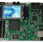
But now ARM and Cadence have shown it doesn’t have to be that way. They recently collaborated to deliver an FPGA-based reference development board. The system includes interface IP from Cadence and the IoT processor subsystem from ARM. From Cadence there is MIPI SoundWIre, Quad-SPI, I2C and SPI. The ARM IP includes a Cortex-M processor, power management, flash cache, flash controller and the Cordio radio. And of course ARM mbed provides the software foundation to manage all of this.
That leaves the solution developer to add sensors, actuators and wireless functionality through provided expansion ports, hardware customization through the FPGA and whatever value-add software applications they feel they need. The development board includes a touch screen with image generation, so the prototype can be completely self-contained (maybe with addition of a speaker and microphone).
One engineer (possibly from ARM, reference material is not clear on this) was able to put together a working IoT sensor prototype in just one month starting from this platform. That’s the kind of turn-around time developers need in a competitive IoT market.
It’s easy to forget in a system like this that a lot of the value in the development system is the pre-proven integration between ARM and Cadence components – the majority of the system, to which you are adding your own special sauce. This isn’t something easy to forget when you put systems like this together yourself. There’s a lot of back and forth discussion with IP providers and anxiety over whether you’re really using IP as expected and whether you’re effectively testing for all possible corner cases.
Much of this is simply lack of enough insight into and experience with those IPs. When IP vendors collaborate to prove out subsystems, as ARM and Cadence have done in this case, most of those problems disappear – they’ve already been considered and resolved by the people most expert in the requirements of their IPs.
That’s really why you can get to a proven prototype in a month. It’s not just that you’re using pre-designed and validated components. It’s that you’re using a pre-designed and validated subsystem where potential issues between different providers of components have already been resolved. That’s worth a lot. I’m betting most of us would like to see more solutions like this. You can learn more about the Cadence/ARM prototype HERE.
HBM controller IP holds the key to bandwidth

We were waiting to see what a different roster including SK Hynix and Synopsys would have to say on HBM in the latest Open Silicon webinar. This event focused on HBM bandwidth issues; a packaging session on 2.5D interposers was promised for a future webinar. Continue reading “HBM controller IP holds the key to bandwidth”
Circuit Simulation Panel Discussion at #53DAC

Four panelists from big-name semiconductor design companies spoke about their circuit simulation experiences at #53DAC in Austin this year, so I attended to learn more about SPICE and Fast SPICE circuit simulation. I heard from the following four companies:
Continue reading “Circuit Simulation Panel Discussion at #53DAC”
High Level Synthesis Update
High-level synthesis (HLS) involves the generation of an RTL hardware model from a C/C++/SystemC description. The C code is typically referred to as abehavioraloralgorithmicmodel. The C language constructs and semantics available to architects enable efficient and concise coding – the code itself is smaller, easier to write/read, and significantly, will compile and simulate much faster than a register-transfer model.
Continue reading “High Level Synthesis Update”
Xilinx is Killing Altera!
At a recent outing with FPGA friends from days gone by, the long running Xilinx vs Altera debate has come to an end. The bottom line is that Xilinx has used the FUD (fear, uncertainty, and doubt) of the Intel acquisition quite effectively against Altera and is racking up 20nm and 16nm design wins at an alarming rate. It will be a while before they all hit HVM (high volume manufacturing) but it is coming, absolutely.
The question I have now is: Will Xilinx be acquired next?
The Intel acquisition of Altera became official in December of 2015 at a cost of $16.7B which was more than a 50% premium based on the stock price when the deal was announced. Altera is the second largest maker of programmable chips (FPGAs), Xilinx (XLNX) being the first.
Altera and Xilinx are fierce competitors in a two horse race for a $5B+ market with an expected CAGR of 8.4% from 2016 to 2020. It is widely recognized in the FPGA world that the vendor who is first to a new process node wins the commanding market share. This was proven when Altera overwhelmingly beat Xilinx to the 40nm process node. Altera was partnered with TSMC (TSM) and Xilinx was partnered with UMC (UMC), UMC stumbled at 40nm and took Xilinx down with them. Prior to 40nm Xilinx was the node leader.
After the 40nm debacle at UMC, Xilinx moved to TSMC (joining Altera) making it a level process node playing field. Xilinx then beat Altera to the 28nm process node by a matter of months and again beat Altera to the 20nm node by more than a year. Xilinx of course was awarded majority market share as a result.
Altera then switched their manufacturing to the new Intel Custom Foundry division for 14nm to better compete with Xilinx. This was a huge PR event as Altera and TSMC were intimate partners since the beginning of the fabless semiconductor transformation in the 1980s. This also brought a direct competition spotlight on Intel versus TSMC for the first time.
Unfortunately Altera stumbled at 14nm and is hoping for high volume manufacturing (HVM) before the end of 2016 while Xilinx started 16nm HVM in 2015. Xilinx also has access to the low cost TSMC 16FFC process to which Intel has no answer so look for additional market share to be won by Xilinx moving forward.
The next process node is 10nm which Intel is currently delaying while TSMC will start 10nm HVM in the first half of 2017 with a quick step to 7nm HVM one year later. Given that quick step, Xilinx has chosen to skip 10nm and move directly to 7nm in 2018. As a result of the challenges Altera experienced with the Intel process bureaucracy at 14nm, I do not expect to see Altera in HVM at Intel 10nm until mid to late 2018, giving Xilinx another solid process advantage.
Will Xilinx be Acquired?
After Intel acquired Altera the rumors started about Xilinx being next. Really it was more about people, like myself, thinking out loud but I would not rule out due diligence and executive level discussions. My take is that Xilinx felt that the Intel/Altera acquisition would falter and favor Xilinx in the long run (which it already has). Xilinx is now in a much stronger position for acquisition discussions with companies that can leverage the dominant position they have in the high margin merchant FPGA market and the desire to compete with Intel in the data center business.
The first name that comes up in the media is Qualcomm but my bet is on Avago/Broadcom CEO Hock Tan. Hock has proven that he can make big deals happen (LSI Logic for $6.6B and Broadcom for a record $37B) and the data center business is in his sights, absolutely.
ARM vs Intel: The New War Frontiers
With Intel’s exit from smartphone processor market, the competitive zones are redefined with its rivalry with ARM. Is ARM’s domination the only reason for Intel’s exit? With no competing architecture, is ARM a monopoly in smartphone processor IP market? What are the new areas of competition between ARM and Intel? I will attempt to answer these questions in this post.
Intel’s exit
I read some news that Intel invested around $10 billion in its mobile processors endeavors. Intel not only invested such huge capital but also digressed from its conventional business model to gather market share. For gaining traction in the low-cost smartphones, SoFIA project was started. In this project, Intel relied on partners, putting aside its vertically integrated business model. Intel partnered with 3rd party SoC design companies for designing SoC on the Atom CPU, and these SoCs would be manufactured in the 3rd party fabs.
It is no brainer to say that ARM is the major reason for Intel’s exit. Can there be some more reasons? In order to compensate for its late entry into smartphone market, Intel paid smartphone OEMs to use its SoCs, and focused on all segments from cost-sensitive volume market to premium segment. The text-book strategy to penetrate a market with dominant incumbent is to focus one customer segment and offer them a complete solution. Did Intel’s strategy match this? I don’t think so. Intel attempted to cater the needs of wide customer segments from high-end to low-end. The solution was not complete, as a competitive integrated modem was missing in some SoCs. I wish Intel would have followed the text-book strategy. It would have been a good experiment to test the credibility of such text-book theories in practice.
Anyways, this is a retrospective discussion for now. Intel also never got any good deal from major OEMs such as Apple, Samsung and Xiaomi. One of the reasons behind this is that all these OEMs have also backward integrated and started designing their own processors. So, x86 is not an option. These companies take architectural license from ARM, and then design the processor as per their needs, and manufacture the processor in fabs such as TSMC, Samsung, etc. The impact of OEMs’ backward integration to pure-play SoC design companies such as Qualcomm, Mediatek, merits a separate analysis. I will try to focus on this in my next post. Open-source systems boost innovation and adoption, as evident from the wide-spread adoption of entities such as Android, Raspberry Pi, Linux, etc. A closed system can never achieve the benefits of network effects, which dictates that value of an entity increases as more users adopt the entity. Intel can never achieve this, as x86 is proprietary.
Also read: Is the Intel Cash Cow in Danger?
Is ARM now a monopolistic power?
With the exit of Intel from smartphone market, ARM is the only company offering IPs for smartphone processors. Does this mean smartphone processor IP market is now a monopoly? Can ARM attract monopolistic rents? With my limited knowledge on microeconomics, I believe the smartphone processor IP market can be modelled as a monopoly, as only one company is active. ARM licenses its IPs to many companies that design processors based on those IPs. ARM makes revenue through licensing cost and royalty. What prevents ARM to dictate prices for smartphone processor IPs?
In my view, there are primarily 3 reasons.
[LIST=1]
New war frontiers
With Intel’s exit from smartphone processor, the areas of competition between Intel and ARM have shifted grounds. Intel will be focusing more efforts on the emerging connected and IoT market. IoT is the next tech tsunami that will drive innovation, competition and market penetration, as smartphone has done so in the last decade. The challenge is that IoT is not a product, it is an ecosystem. Apart from the software offerings such as cloud management, APIs, data analytic, etc., at the hardware level it needs sensors or end-nodes, gateways, server or data center, and connectivity devices.
At the front-end or customer-facing end of IoT applications are connected things or sensors, that tracks or monitors some ambient conditions. These end-nodes or frugal devices will be scattered in all places from light bulbs, vehicles, building, elevators, industrial plants, oil refineries, and many more. The data collected from the ambient environment will be passed on to gateways that may do some processing on the data. The data is pushed from the gateways to servers, in which advanced data analytic can be done on petabytes of data. Cloud services plays a vital role in this chain from data collection, reception and analysis. Each of the hardware involved in the chain including sensors, gateways, and servers will be having some processing unit, memory and some I/Os depending on their usage.
Sales volume will be driven by end-nodes or sensors that will be needed in billions for collecting vital information from various surroundings. To drive mass adoption, these end-nodes should be low-cost; however, due to application-specificity and customer-specificity, the sales volume for individual SKUs will be less. COTS processors may not fulfill all the requirements of power, performance, price and space of the end-nodes. The focus will be on application-specific processor that is tuned to the needs of the specific industry. Companies building IoT products would be more interested in custom processors that are tuned to their requirements and budget. However, the problem is to fulfill the conflicting objectives of customization and low-cost. Any company solving this problem will crack the IoT market.
Now coming to the competition in the end-nodes business between ARM and Intel. Intel offers Quark SoC and micro-controllers that can be used for the end-nodes or connected things. In a recent blog after its restructuring, Intel made clear that it will work towards offering a complete ecosystem for IoT: frugal connected things, servers, networking and cloud services. However, one thing that I fail to understand yet is how Intel will control the cost structure of Quark or similar processors, without making business loss? With its vertically integrated business model, it is difficult to achieve cost-optimization. Further, off-the-shelf processors may not be ideal for many IoT applications.
In past, for capturing low-cost smartphone market, Intel sidelined its vertically-integrated business model and started the SoFIA project, in which it partnered with Chinese design companies for the SoC design and then get the SoC manufactured at pure-play foundries. The idea was to cost-control that is not possible with the high-margin Intel’s business model. Shall Intel pursue a similar program for low-cost processors targeted for the connected things? I believe, it is worth a try.
However, the second issue that may erupt with the above strategy is that COTS processors may not be an ideal choice for many IoT applications. ‘One processor fit all’ may not hold good for IoT market, as the applications are diverse in terms of usecase, power, performance, and I/Os. With proprietary x86, it is not possible to build customized SoCs. Should Intel start licensing x86 architecture? This is a difficult question to answer, for me at least. However, I strongly believe in the power of network effects, collaboration and coo-petition. All these cannot be possible with closed standards. AMD has already started licensing x86 server IPs. I am sure that Intel will have to deal with more competitors in the near future. What do you think on how Intel can address this issue?
On the other hand, ARM is steadily carving an IoT ecosystem. Already being used in billions of smartphones and embedded devices, ARM may have an edge over Intel in the IoT market currently. With IP licensing model, system designers can differentiate their products from those of competitors by designing processors according to their budget, form-factor and application requirements. This offers better control to companies to target niche segments of IoT. ARM has realized that mass-scale production by large SoC vendors will not bring radical innovation in IoT space, instead value-addition will be driven by small companies that focus on niche markets.
With ARM DesignStart program, ARM is lowering the entry barrier for custom SoC design and manufacturing on Cortex-M0 IP. This program offers low-cost access to Cortex-M0 IP along with design services (from Cadence, & Mentor Graphics) and physical IPs. This will promote further penetration of ARM IPs among start-ups, design enthusiasts, etc. Designers can start their development with limited fixed cost. After evaluation, they can go for full-scale production at nominal cost. This will enable low-cost products targeted to hundreds of niche IoT applications.
Further, ARM also aspires to capture market share in server space. Presence in server space will be enable a full-scale IoT value chain: end-devices (Cortex M series), gateways (Cortex A9, A15 etc. in vehicles, medical, & many more), servers (64 bit processors) and software (mbed, Cloud services).
Conclusion
Interesting times are coming ahead. Both companies, along with many others will compete to realize the billions of connected devices. I strongly believe most innovation will happen at small companies and start-ups, rather than in large companies. The strategy should be address the needs of these thousands of small companies by offering a base that is cost-effective and scalable.
I really look forward to your views, suggestions and improvement areas. I would like to emphasize that these are completely personal views with my limited knowledge. I do not have any professional or business interests with any organization mentioned in this post. I also encourage you to take a look a look at my earlier blogs on ARM vs Intel:
ARM vs Intel – Not a tech war
ARM vs Intel – The way further
It’s Time to Put Your Spice Netlists on a Diet
Spice circuit simulation remains the backbone of IC design validation. Digital cell library developers rely upon Spice for circuit characterization, to provide the data for Liberty models. Memory IP designers utilize additional Spice features to perform statistical sampling. Analog and I/O interface designers extend these requirements into frequency-domain analysis, using parameter sweeps. Across all these domains, focusing on optimizing Spice simulation throughput is crucial.
Yet, technology trends are exerting pressure on circuit simulation performance. The number of PVT corners is growing significantly. From a design perspective, the number of operating voltage conditions is increasing, as dynamic voltage frequency scaling (DVFS) methods are more widely applied. The number of process-based corners is also growing, driven in large part by the additional variation associated with lithographic multi-patterning overlay tolerances. Each multi-patterned layer now exhibits a variation range in coupling capacitance between adjacent wires which have been decomposed to separate masks for the layer.
And, a major increase in the number of layout-extracted parasitic elements has emerged in current technologies, due to the addition of dummy devices adjacent to active transistors, the additional of local interconnect layers (prior to contacts and M1), and the increased number of metal and via layers. Specifically, these parasitic elements have a growing impact on circuit performance, as scaling of the physical width and cross-sectional area of the associated wires and vias has continued.
All these factors have increased the Spice simulation workload. And, the annotation of extracted parasitics to the original schematic netlist reduces the simulation performance substantially.
To address these trends, Spice simulation tools have incorporated performance enhancements – e.g., parallel thread execution, “fast” execution using simplified device models, and “event-driven” solvers for analysis of sparsely-active circuits. Yet, these approaches all have an associated cost, whether it be an accuracy versus performance tradeoff, or simply the licensing costs for these different tools to fulfill the simulation requirements.
Fundamentally, the first step should be to optimize the parasitic-annotated netlist, to get the best overall performance regardless of the simulation method. Although layout extraction tools offer options to adjust the accuracy and size of the resulting parasitic model, an attractive methodology would be to extract at the highest accuracy setting, then subsequently optimize this netlist for the target applications.
At the recent DAC conference, I had the opportunity to meet with Jean-Pierre Goujon, Application Manager at edXact. He was enthusiastic about two recent events:
(1) the increasing customer adoption of their parasitic reduction technology, and
(2) the recent acquisition of edXact by Silvaco, which will further expand their market presence (and from Silvaco’s perspective, continue their recent emphasis on broadening their product portfolio)
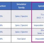
The focus for edXact has been on algorithmically-robust methods for reduction of large parasitic networks to improve Spice simulation throughput, while maintaining (user-controlled) accuracy of the results. Their approach applies rigorous model-order reduction methods, preserving input/output pin impedance, pin-to-pin resistance, and pin-to-pin delay. The netlist size reduction and thus the simulation speedup examples Jean-Pierre highlighted were impressive – please refer to the figure below.
Note that both full and “fast” Spice simulation tools reap the benefit of the optimized netlist. (According to Jean-Pierre, a “typical” runtime for model-order reduction on an IP block would be about one CPU-hour.)
There are additional edXact options available to designers, to further enhance simulator performance. For example, for some (digital cell) simulation applications, there are less stringent characterization requirements – the accuracy required for delay arcs in DFT scan mode come to mind. Reduction options can be selectively set by the designer for different nets. As illustrated below, specified “critical nets” maintain the highest accuracy (most conservative reduction), while non-critical nets can be more aggressively reduced.
I tried to trip up Jean-Pierre, asking “What about the various data formats used by different Spice simulation and extraction tools?”
“No problem.”, he replied. “We support all major simulator and parasitic netlist formats for actives and passive elements – Spice, Spectre, DSPF, SPEF, SPF, CalibreView, with R, C, L, and K parasitics. The tool is easily integrated into existing design platforms and flows.”
He added (with a smile), “And, don’t forget the temperature coefficients of resistance on extracted wires – TC1 (first order) and TC2 (second order). We adjust these coefficients on the reduced netlist to maintain the same overall temperature dependence.”
I then posed my toughest question, “How would a customer ‘qualify’ the netlist reduction technology in their design environment?”
Jean-Pierre answered, “We have a separate tool for qualifying results, providing users with visual, analytical feedback on the comparisons between the original and reduced netlists. We compare the effective delay between pins. And, the pin-to-pin resistance is also a critical metric.”
When forecasting the Spice simulation resources required for your next design project — i.e., software licenses, server CPU’s and memory, target throughput/schedule — it would be appropriate to ensure that optimized post-extraction netlists are the norm for your design flows. An investment in model-order reduction technology will very likely provide an attractive ROI, with minimal impact on the accuracy of the simulation results.
For more information on the edXact reduction technology, please refer to this link.
-chipguy
The amazing artificial intelligence we were promised is coming, finally
We have been hearing predictions for decades of a takeover of the world by artificial intelligence. In 1957, Herbert A. Simon predicted that within 10 years a digital computer would be the world’s chess champion. That didn’t happen until 1996. And despite Marvin Minsky’s 1970 prediction that “in from three to eight years we will have a machine with the general intelligence of an average human being,” we still consider that a feat of science fiction.
The pioneers of artificial intelligence were surely off on the timing, but they weren’t wrong; AI is coming. It is going to be in our TV sets and driving our cars; it will be our friend and personal assistant; it will take the role of our doctor. There have been more advances in AI over the past three years than there were in the previous three decades.
Even technology leaders such as Apple have been caught off guard by the rapid evolution of machine learning, the technology that powers AI. At its recent Worldwide Developers Conference, Apple opened up its AI systems so that independent developers could help it create technologies that rival what Google and Amazon have already built. Apple is way behind.
The AI of the past used brute-force computing to analyze data and present them in a way that seemed human. The programmer supplied the intelligence in the form of decision trees and algorithms. Imagine that you were trying to build a machine that could play tic-tac-toe. You would give it specific rules on what move to make, and it would follow them. That is essentially how IBM’s Big Blue computer beat chess Grandmaster Garry Kasparov in 1997, by using a supercomputer to calculate every possible move faster than he could.
Today’s AI uses machine learning in which you give it examples of previous games and let it learn from those examples. The computer is taught what to learn and how to learn and makes its own decisions. What’s more, the new AIs are modeling the human mind itself using techniques similar to our learning processes. Before, it could take millions of lines of computer code to perform tasks such as handwriting recognition. Now it can be done in hundreds of lines. What is required is a large number of examples so that the computer can teach itself.
The new programming techniques use neural networks — which are modeled on the human brain, in which information is processed in layers and the connections between these layers are strengthened based on what is learned. This is called deep learning because of the increasing numbers of layers of information that are processed by increasingly faster computers. These are enabling computers to recognize images, voice, and text — and to do human-like things.
Google searches used to use a technique called PageRank to come up with their results. Using rigid proprietary algorithms, they analyzed the text and links on Web pages to determine what was most relevant and important. Google is replacing this technique in searches and most of its other products with algorithms based on deep learning, the same technologies that it used to defeat a human player at the game Go. During that extremely complex game, observers were themselves confused as to why their computer had made the moves it had.
In the fields in which it is trained, AI is now exceeding the capabilities of humans.
AI has applications in every area in which data are processed and decisions required. Wired founding editor Kevin Kelly likened AI to electricity: a cheap, reliable, industrial-grade digital smartness running behind everything. He said that it “will enliven inert objects, much as electricity did more than a century ago. Everything that we formerly electrified we will now ‘cognitize.’ This new utilitarian AI will also augment us individually as people (deepening our memory, speeding our recognition) and collectively as a species. There is almost nothing we can think of that cannot be made new, different, or interesting by infusing it with some extra IQ. In fact, the business plans of the next 10,000 start-ups are easy to forecast: Take X and add AI This is a big deal, and now it’s here.”
AI will soon be everywhere. Businesses are infusing AI into their products and helping them analyze the vast amounts of data they are gathering. Google, Amazon, and Apple are working on voice assistants for our homes that manage our lights, order our food, and schedule our meetings. Robotic assistants such as Rosie from “The Jetsons” and R2-D2 of Star Wars are about a decade away.
Do we need to be worried about the runaway “artificial general intelligence” that goes out of control and takes over the world? Yes — but perhaps not for another 15 or 20 years. There are justified fears that rather than being told what to learn and complementing our capabilities, AIs will start learning everything there is to learn and know far more than we do. Though some people, such as futurist Ray Kurzweil, see us using AI to augment our capabilities and evolve together, others, such as Elon Musk and Stephen Hawking, fear that AI will usurp us. We really don’t know where all this will go.
What is certain is that AI is here and making amazing things possible.
For more, follow me on Twitter: @wadhwa and visit my website: www.wadhwa.com
Network generator embeds TensorFlow, more CNNs
Research on deep learning and convolutional neural networks (CNNs) is on the rise – and embedding new algorithms is drawing more attention. At CVPR 2016, CEVA is launching their 2[SUP]nd[/SUP] generation Deep Neural Network (CDNN2) software with new support for Google TensorFlow. Continue reading “Network generator embeds TensorFlow, more CNNs”