For Halloween this week we thought it would be appropriate to talk about things that strike fear into the hearts of semiconductor makers and process engineers toiling away in fabs. Do I want to do multi-patterning with the huge increase in complexity, number of steps, masks and tools or do I want to do EUV with unproven tools, unproven process & materials and little process control?
Continue reading “Choosing the lesser of 2 evils EUV vs Multi Patterning!”
Effective Project Management of IoT Designs
ClioSoft is well known for their SoC design data management software SOS7 and more recently for their IP reuse ecosystem called designHUB. What is less known is how designHUB enables design teams to collaborate efficiently and better manage their projects by keeping everyone in sync during development. Not only does it provide a platform for design teams to more easily integrate IPs into their designs and collaborate more efficiently, but it also enables cooperation among diversified groups that normally would not work that closely together. This is an essential element of project management for complex systems-on-chip (SoC) and systems-in-a-package (SiP) designs.
With the advent of the Internet-of-Things (IoT), systems are becoming much more complex as they use heterogeneous system architectures both on the SoC and within a package. These systems can have multiple different CPU cores, hardware accelerators, memories, network-on-chip (NoC) fabrics and numerous peripheral interfaces. Added to this are the complexities of the package, interposer and production board, not to mention boards designed for silicon bring-up and for prototyping. IoT system projects can have hundreds of engineers with different backgrounds and expertise working on them. The question then becomes how to manage and coordinate efforts between system designers, software engineers, IC designers, package and interposer designers, design-for-manufacturing (DFM), design-for-test (DFT) and test engineers.
ClioSoft’s designHUB turns out to be an excellent platform to bring these diverse groups together. When design data management is discussed we tend to gravitate to the various design data formats that needs to be shared between groups. We forget however that there is a much larger set of data represented by the knowledge base of the engineers that create the design. Additionally, for any given function, there is meta data about the function such as specifications, verification methodologies, test methodologies and manufacturing assumptions to which that function is being designed. This is true whether you are designing hardware logic, embedded software, NoCs, or last-level cache memories for the system. ClioSoft’s designHUB provides a rich environment that allows data of any form to be documented, versioned, stored, linked to other dependent data, searched and retrieved.
The unique thing about designHUB is that it provides a dashboard that tracks all activities in which an engineer is involved. The dashboard gives each designer a customized experience that can be set up to notify them upon specific events that may impact their work.
As an example, if a software developer is writing a device driver that is dependent upon some custom logic, and details for that custom logic are changed, designHUB can be set up to instantly notify the software developer of the changes. The software developer would have access to a knowledge base for the design part in question, where they could get details about the changes that occurred. Similarly, impacts to the developer’s code may propagate on to system test engineers who are working on the modules that will be used to validate the device driver once parts are back from manufacturing. Schedule changes can also be propagated to those with dependencies as well as to a master schedule that is reviewed by project management.
ClioSoft’s designHUB also has a social media component to it that allows for crowdsourcing type interactions. Open questions can be asked of the project with anyone in the project being able to share their insights and knowledge. All knowledge shared becomes part of the knowledge database for the project as well as for the part of the design that is being discussed. Some subjects such as verification and test tend to cut widely across a project. Proposed changes in these types of areas can be quickly discussed. Management can also play a part in these discussions enabling fast decision making and easier dissemination of policy changes to project team members using the communications capabilities of designHUB.
The best part of all this interaction is that the conversations and data are preserved for the next revision of the project or for derivative designs that may use parts of the current project. Not only is the basic design data stored and versioned, but also the meta data about the design including dependency relationships between different modules. This means that project managers can track the impact of proposed changes to modules to gauge the impact of a desired change and to check that affected areas are indeed re-verified to ensure the new changes have not inflicted collateral damage in other parts of the project. In addition, if a designer leaves the company the design knowledge remains captured within designHUB thereby protecting the company from any major problems.
Lest this sound a little too open or lacking in controls, rest assured that you can also use designHUB to enable workflows with approval and signoff procedures for the various design objects such as IPs, documents etc.. ClioSoft’s designHUB can also track time through various project phases which can later be used for post tape-out lessons-learned reviews. The idea here is to make decisions as transparent as possible without giving way to total anarchy. Projects are still “managed” but it becomes much easier for management and engineering teams to make informed decisions and to stay abreast of changes being made to the project that might affect them.
All in all, designHUB is a great suite of tools that is only just beginning to see reveal some of its features and use models. For now, we can check off IP management and Project management. It will be interesting to see what users come up with next.
See also:
ClioSoft designHUB web page
ClioSoft designHUB webinar
Using a TCAD Tool to simulate Electrochemistry
In college I took courses in physics, calculus, chemistry and electronics on my way to earn a BSEE degree, then did an 8 year stint as a circuit designer, working at the transistor level and interacting with fab and test engineers. My next adventure was working at EDA companies in a variety of roles. As a circuit designer I knew that we had software tools like SPICE to help us simulate the timing, power, currents and detailed operation of transistor devices, cells, blocks and modules. What I’ve come to learn about is that device technology engineers also need software tools to help them simulate electrical, chemical, optical and thermal behavior of semiconductor devices. Silvaco recently held a webinar on Wednesday, so I attended to learn about TCAD Simulation of Ion Transport and Electrochemistry.
Very quickly I learned the definition of Electrochemistry by our presenter Dr. Carl Hylin.
Electrochemistry describes the chemical interactions between electrons, holes, ions and uncharged chemical species.
I felt pretty comfortable as an EE to hear familiar terms like electrons, holes and ions, but chemical species was a new term for me. There are at least four major applications where knowing what is happening at the electrochemical level is mandatory:
- Standard semiconductor devices
- Shockley-Read-Hall (SRH) recombination
- Auger recombination
- Charge trapping
- Displays
- Degradation in amorphous TFTs
- Spacecraft electronics
- Enhanced low-dose-rate sensitivity
- Non-volatile memories (RRAM), solid state batteries
- Ion transport and charge storage
Silicon, Germanium, Gallium and Arsenide materials are all examples of a chemical species. Equations have been derived that define how chemical species behave, and that forms the basis for apply software like the Silvaco simulator called Victory Device:
When using the Victory Device tool you first define the materials (species) and then the type of reaction you want to simulate. For example if you wanted to model and simulate the compound semiconductor made up of Indium, Gallium and Zinc (InGaZn) using Victory device then it’s only a few lines of coding, shown below in colored letters:
With this device simulator you can define as many species as needed, and you get to define the names of the species in terms that are self-documenting. Doping levels are also defined, along with the interface between species, so here’s another example using two chemical species: Silicon (Si) and Hydrogen (H).
For our example of SiH we also define properties like diffusivity and the maximum species concentration, with units of atoms/cm^3 :
Silicon is a fixed species, meaning that the diffusivity is zero, however Hydrogen has a non-zero diffusivity and is transportable. Here’s a Lewis diagram showing Hydrogen on the left and Si plus SiH on the right:
Mobile species can hit a boundary and be blocked, so that there’s no transport. In Victory Device you define at what concentration level a species may transport, here’s an example with Hydrogen using a fixed concentration amount:
To model and simulate the passivated interface degradation with the SiH material it takes just 16 lines of code in Victory Device:
The results of simulation can be viewed in a couple of ways, wither a structured file output or a log file output. The final example from the webinar was showing Victory Device was used for predicting the negative bias stress simulation with illumination in a TFT made up of Indium, Gallium, Zinc and Oxide. Simulation results correlated well with published data, this graph shows the Vt shift by NBIS for a 20nm IGZO TFT device where red curves are measured results and blue is from simulation:
With device simulation there are always more demands, so the engineers at Silvaco are adding new abilities to their road map for Victory Device, like:
- Constant surface velocity and constant flux boundary conditions
- Vacancies
- Thermochemistry
- Steady-state simulation
- Added reaction models
- Added mobility models
- Improved automatic time-step control
Summary
In the old days the device technology engineer would make many physical experiments, wait for the wafers to get through the line, then make measures to decide if more iterations were required before reaching a stable process. With the advent of TCAD tools like Victory Device we can now perform many device simulations in a virtual world based on the laws of physics and chemistry, thus shortening time to market and creating a more reliable semiconductor process.
To replay the entire 45 minute webinar you may register online now.
Related Blogs
Design Data Intelligence
We have an urge to categorize companies, and when our limited perspective is of a company that helps with design, we categorize it as an EDA company. That was my view of Magillem, but I have commented before that my view is changing. I’m now more inclined to see them more as the design equivalent of a business intelligence organization – an Oracle or SAP or SalesForce, something along those lines – kind of a design intelligence company. I’m not suggesting Magillem has the scale or reach of those business organizations but it does seem to have a similar mission, within the world of system design.
I was at the Magillem user group meeting recently to understand where they are headed and what users think of what they are doing. Isabelle Pesquie-Geday, the CEO, opened with a business summary, always useful to check reality is headed in the right direction to support the vision. Last year revenues grew 24%, strategic projects are growing (unsurprising when they are in this line of business), they now have a branch in Shanghai, a subsidiary in Korea and have added staff in the US. Business today is geographically split quite evenly between the US, Europe and Asia and is predominantly today with semiconductor companies, with a smaller component in systems companies and a still smaller component in publishing (remember that one).
Back to technology. To leverage design intelligence, you have to start with a common core format. Magillem is best known for their support of XML-based tools, in the design domain supporting the IEEE-1685 (IP-XACT) standard for design representation. This standard data representation is the core of how they manage linkages between components in a system, certainly for blocks/IPs and the connectivity between these but also between system level dependencies – hardware and software views, different levels of abstraction from requirements to architecture, to implementation, documentation, specifications and traceability.
An important point to understand is that the IEEE standard doesn’t aim to replace existing representations of design (eg RTL) or documentation which are already well-handled in existing formats. Rather the goal is to package and link these representations to support easy interoperability between different levels of abstraction in design data models, connections between hardware and software characteristics and, thanks to an open-standard format, to encourage high levels of automation in assembly and verification / validation of these systems. The standard replaces or encapsulates many of these total system design objectives (otherwise described in proprietary side-files) through standard XML schemas.
So what’s the ground truth; how is the standard working out in active SoC design today? At the user-group meeting there were presentations from NXP, Bosch and Renesas and there were attendees from multiple other companies including, interestingly, a well-known supplier of PCB software. In deference to confidentially expectations at these organizations, I won’t detail who said what but I will mention what for me were some important takeaways.
It should be pretty obvious that there is active use among companies working in automotive supply chains, and it’s not difficult to imagine why they might want to pursue this direction. A common standard, auditable format between suppliers should be appealing to show advantages in certification over suppliers with less structured and proprietary data formats. Also I can imagine traceability above the chip level can be challenging if suppliers aren’t using common formats. Through an open standard it should be easier to demonstrate traceability of requirements and impact of changes. Magillem already has a track-record in working with aerospace organizations in Europe where this type of consideration is extremely important.
For all the presenters, these flows have been in production for multiple years. Usage varies from fast and reliable assembly of the SoC top-level with easy configurability to drive multiple verification flows from simulation to RTL prototypes, register / memory-map validation, document generation and update, all the way to all of these plus configurable modeling with mixed views (TLM, RTL, gate).
These are the “classic” applications of IP-XACT-based flows, but where can this lead next? An obvious next step is into traceability. Magillem has already made progress in this direction with their Magillem Link Tracer (MLT). They continue to evolve their traceability goals, moving closer to bi-directional support for linkages between multiple different “documents” in the system definition from specification and requirements to documentation, design representation and verification / validation views. Here the trick is how many of these linkages must be defined manually and how many can be inferred automatically. The IEEE standard takes care of some of this. Connections to documentation for example are still challenging, but read on.
This is where Magillem’s interest in AI starts. They are quite modest about their goals in this area – to develop assistants to help in the system development task rather than any high-flown “robot designer” kind of vision. Dr. Eric Mazeran (IBM) gave a very good background to this area which I hope to summarize sometime in a separate blog. Eric has been in the AI field for 25 years (largely in AI applications to business intelligence) and, when not working his full-time job with IBM, consults with Magillem. Here I’ll touch on just a couple of Magillem applications areas he introduced with Isabelle.
The first is in support of legal publishing – updating legal documents to reflect daily updates based on decrees and other official sources of changes. This is not even remotely in the design domain but is has an interesting adjacency. Briefly, the legal solution combines natural language processing (NLP), deep learning and a references-indexing engine to tag (eg. insert or edit) required changes, compare this to mountains of legal documents to which these changes might apply, then generate suggested edits to appropriate documents. Note “suggested”. The tool doesn’t make the changes itself; there is still a human editor in the loop to check the proposed changes. The tool acts as an assistant to the editor, solving the massive combinational part of the problems – millions of comparisons – to boil down a limited set of changes the editor must consider.
A similar application could help build links between ad-hoc documents and design representations, which then can be tracked in traceability analyses. Magillem is also exploring decision-tree-based expert systems to capture common types of expert knowledge within an organization. These are often problematic because there are too few experts who need to work with too many product teams and there is significant risk when an expert leaves the company. Eric showed a manufacturing example in his talk where a production supervisor walked through a Q&A with such an assistant to diagnose a problem and explore possible corrective actions. Again, the assistant helped the supervisor to get to a workable set of options, from which she could recommend next actions. You could imagine all kinds of hard-earned expertise in production design flows being captured in a similar way.
Quite an ambitious reach, starting from something as seemingly mundane as an industry-standard XML data format for system integration data. You can learn more about Magillem solutions HERE.
Synopsys discusses the challenges of embedded vision processing
Before the advent of convolutional neural networks (CNN), image processing was done with algorithms like HOG, SIFT and SURF. This kind of work was frequently done in data centers and server farms. To facilitate mobile and embedded processing a new class of processors was developed – the vision processor. In addition to doing a fair job of recognition, they were good at matrix math and pixel operations to filter and clean up image data or identify areas of interest. However, the real transformation for computer vision occurred when CNN won the ImageNet Large Scale Visual Recognition Challenge in 2012. The year before a the winning non-CCN approach achieved an error rate of 25.8%, which was considered quite good at the time. In 2012 the CNN called AlexNet came in first with an error rate of 16.4%.
Just three years later by 2015, CNN moved up to an error rate of 3.57%, exceeding the human error rate of 5.1% on this particular task. The main force behind ImageNet is Stanford’s Fei-Fei Li, who pioneered the ImageNet image database. Its size exceeded by many orders of magnitude any previous classified image database. In many ways, it laid the foundation for the acceleration of CNN by providing a comprehensive source of training and testing data.
In the years since 2012 we have seen tremendous growth in the applications for CNN and image processing in general. A big part of this growth has taken computer vision out the server farm and moved it closer to where image processing is needed. At the same time the need for speed and power efficiency has increased. Computer vision is used in factories, cars, research, security system, drones, mobile phones, augmented reality, and many other applications.
At the Linley Processor Conference in Santa Clara in October Gordon Cooper, embedded vision product marketing manager at Synopsys, talked about the evolution of their vision processors to meet the rigorous demands of embedded computer vision applications. What he calls embedded vision (EV) is different than traditional computer vision. EV combines computer vision with machine learning and embedded systems. However, EV performance is affected by increasing image size and frame rates. Also, power and area constraints need to be dealt with. Finally, technology is rapidly advancing. If you look at the ImageNet competition, you will see that each year the core algorithm has changed dramatically.
Indeed, approaches for CNN have evolved rapidly. The number of layers has increased from ~ 8 to over 150. At the same time hybrid approaches are becoming more prominent by using a fusion of computer vision and CNN techniques. To assist in these newer approaches, Synopsys is offering heterogeneous processing units in their EV DesignWare® IP. These consist of scalar, vector and CNN processors in one integrated SOC IP. The Synopsys DesignWare® EV6x family offers from 1 to 4 scalar and vector processors combined with a CNN engine. This IP is supported by a standards-based software toolset with OpenCV libraries, OpenVX framework, OpenCL C compiler, C++ compiler and a CNN mapping tool.
The processing units are all connected by high speed interconnect so operations can be pipelined to increase efficiency and parallelism during frame processing. The EV6x family supplies a DMA Streaming Transfer Unit that facilitates data transfers to speed up processing. Here is the system block diagram for the vision CPU’s.
The EV6x IP is completed with the addition of the CNN880 engine. It is programmable to support a full range of CNN graphs. It can be configured to support 880, 1760 or 3520 MAC’s. Implemented in 16nm running at 1.28GHz it is capable of 4.5 TMAC/s under typical conditions. As for power efficiency, it delivers better than 2000 GMAC/s/W.
By combining the capabilities of traditional vision CPU’s with a CNN processor, the EV6x processors can achieve much higher efficiency than either alone. For instance, traditional vision processors can remove noise and perform adjustments on the input stream, improving the efficiency of the CNN processor. Also, the vision processors can help with area-of-interest identification. Finally, because these systems operate in a real-time environment, the additional processing capabilities of the EV6x can be used for taking action on the image processing results. In autonomous driving scenarios, immediate higher level real-time action may be required, such as actuating steering, braking or other emergency systems.
Embedded vision is an exciting area right now and will continue to evolve rapidly. It’s not enough to have recognition or in some cases even training done in a server farm. All the activities related to computer vision will need to be mobile. This requires hybrid architectures and computational flexibility. Any system fielded today will probably see major software updates as training and recognition algorithms evolve. Having a platform that can adapt and is easy to develop on will be essential. Synopsys certainly has taken major steps in accommodating today’s approaches and future-proofing their solutions. For more information on Synopsys computer vision IP and related development tools, please look at their website.
Electronic Design for Self-Driving Cars Center-Stage at DVCon India
The fourth installment of DVCon India took place in Bangalore, September 14-15. As customary, it was hosted in the Leela Palace, a luxurious and tranquil resort in the center of Bangalore, and an excellent venue to host the popular event.
As reported in my previous DVCon India trip reports, the daily and evening traffic in Bangalore is horrible, and a dramatic contrast to the empty roads in the middle of the night when overseas travelers arrive or leave the country. Congested roadways forced conference management to delay the beginning of the event by 30 minutes to accommodate the slow arrivals of the participants.
The mornings of the two-day conference included keynotes and panels. The two-day afternoons were packed with 13 tutorials, 39 papers, and nine posters. Sessions covered various aspects of the design verification processes, from electronic system level (ESL) to design verification (DV), the majority focused on UVM, formal, and low power with an eye on safety in automotive chip design. Hardware/software co-verification and portable stimulus were also covered.
The conference kicked off with a keynote address by Chris Tice, vice president of Verification Continuum Solutions at Synopsys, titled “The Peta Cycle Challenge.” For the mathematically challenged, probably none among the highly educated Indian engineers, it equates to 10^15, or a quadrillion cycles. The presentation started with a set of case studies from different segments of the electronic industry that proved the need for peta cycles for thorough design verification/validation. Rather interesting stuff. Unfortunately, the presentation turned into a sales pitch for the Synopsys’ Verification Continuum with emphasis on emulation and FPGA prototyping that did not belong to a keynote. By the way, I wonder why Synopsys has not supported Chris’ statement “emulators based on commercial FPGAs have a refresh rate of two years versus the four/five years of the custom-hardware-based counterparts.” After all, the yet-to-be announced next generation of the Synopsys’ ZeBu emulator based on commercial FPGAs lags already almost four years behind the launch of the Xilinx UltraScale in December 2013.
Mr. Tice’s keynote was followed by an invited keynote titled, “Re-emergence of Artificial Intelligence Based on Deep Learning Algorithm,” delivered by Vishal Dhupar from NVIDIA. Mr. Dhupar traced the similarities in the evolution of self-driving cars, drones and robots as the result of deep learning, a fast growing field in artificial intelligence.
Following Mr. Dhupar’s insightful comments were two more invited keynotes. Manish Goel from Qualcomm India discussed “System-level Design Challenges for Mobile Chipsets,” and Apurva Kalia reviewed the evolution of the self-driving car in his “Would you Send Your Child to School in an Autonomous Car?” presentation.
Two panels, one on ESL and the other on DV, concluded the first morning. I moderated the DV panel, titled “Hardware Emulation’s Starring Role in SoC Verification.” Panelists included Sundararajan Haran of Microsemi; Ashok Natarajan from Qualcomm; Ravindra Babu of Cypress; and Hanns Windele from Mentor, a Siemens Business. All shared their views on the evolution of emulation in the design verification flow. A write-up summarizing the experiences and opinions of the panelists will follow shortly.
The keynote on the second day was delivered by Ravi Subramanian of Mentor and titled “Innovations in Computing, Networking, and Communications: Driving the Next Big Wave In Verification.” First, Mr. Subramanian using several data points pointed out that recent semiconductor industry structural changes are about specialization, not consolidation. He then showed that a growing captive semiconductor market is emerging in system houses. For example, MEA (More Electrical Aircraft) is disrupting the aircraft industry via electrification and automation of the entire airplanes. This was followed by an analysis of the convergence of, and key trends in computing, networking and communications. According to Mr. Subramanian, convergence is posing a big challenge in functional verification, forcing the industry to rethink its approach.
As a nice touch, Mr. Subramanian complimented the Indian engineering community, said to lead the worldwide adoption of the SystemVerilog design language and the UVM design methodology.
An invited keynote titled, “Disruptive Technology That Will Transform The Auto Industry,” was presented by Sanjay Gupta, vice president and country manager at NXP. It was an impressive talk supported by lots of interesting data. Unfortunately, keynotes’ slides were not made available to the attendees. I would kindly ask the DVCon/India committee to make them available in future events.
On the exhibit floor 15 EDA companies demonstrated their verification tools and methodologies. The vendors list included the big three –– Cadence, Mentor and Synopsys ––as well as Aldec, Breker, Chipware, Circuit Sutra, Coverify, Doulos, SmartDV, TVS, Thruechip, Verifast, Verific, and Verifyter.
DVCon India 2017 was a successful conference, crammed with useful information, and a great networking opportunity. As usual, the Indian hosts were cordial and humorous.
The 2017 round of DVCon conferences organized by Accellera will conclude with DVCon Europe in Munich, Germany, October 19-20.
1st Annual International Conference, Semiconductors ISO 26262
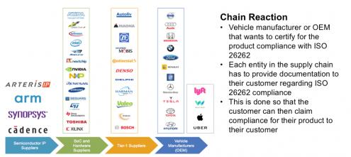
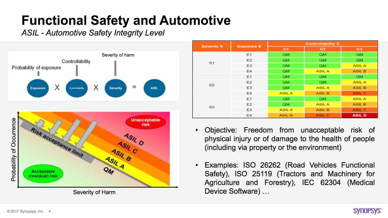
When we talk about the promise of ADAS and autonomous cars then along the way we also hear about this functional safety standard called ISO 26262 which semiconductor companies all pay close attention to. I recently learned about a new conference called Semiconductors ISO 26262, scheduled for December 5-7 in Munich, Germany. The conference chairman is Riccardo Mariana, Intel Fellow, Functional Safety.
The aim of the conference is to help semiconductor companies meet the automotive safety challenges by:
- Sharing the latest updates on ISO/DIS 26262:11 for competitive edge in functional safety.
- Discussing improvements of the semiconductor usage in safety-critical systems for higher integrity level.
- Discovering innovations in highly automated driving that the semiconductor sector can benefit from.
- Addressing confidence issues in the use of software tools specifically designed for semiconductors challenges.
- Analyzing fault injection tools to support safety analysis.
- Finding diverse approaches to handle the safety of multicore.
There are 20 speakers lined up for this conference (Intel, NVIDIA, Renesas, Melexis, NXP Semi, Xilinx, ST Micro, TI, Toshiba, Qualcomm, Resiltech, Arteris, Robert Bosch, SGS-TUV, Brose Fahrzeugteile, ARM, Infineon, Harman International, Sensata Technologies, NetSpeed Systems, Jama Software) and one of them is from my locale in Portland, Oregon: Adrian Rolufs, Senior Consultant at Jama Software. I was able to correspond with Trevor Smith of Jama Software to get the big picture of ISO 26262 and how Jama Software is used by automotive engineers for product definition, change management and functional safety verification.
What makes Jama software stand out from competitors?
Our customers choose Jama for a number of reasons but the key factors typically include our extremely easy to use interface which drives high adoption rates among product development teams. Additionally that ease of use allows teams to build the solution around and along with their development process and not completely change their process to use a specific type of tool. This leads teams to quickly adopt Jama in both the regulated industries like automotive and the non-regulated industries like mobile phones. Companies can unify their development process across the entire company and not have silo’d development within each product line.
Based on your point of view, what challenges are semiconductor companies facing in order to comply with ISO 26262?
With the unprecedented growth that is forecasted for semiconductor suppliers in the automotive market, it has brought new players to the space who in the past have not been responsible for the stringent regulations that the automotive market demands. These new players are still facing the extremely competitive market that semi companies typically face but now require them to add more rigor to their entire product development process in order to support this market. And this isn’t only for new players, older automotive suppliers are seeing increased competition because of the projected growth, these existing players also need to step up their game to deliver products on time but still keeping a close eye to the functional safety regulations that ISO 26262 places on them.
How can Jama help solve the above challenges?
At Jama we keep a very close eye on the trends that are facing not only semiconductor designers and manufacturers, but also many of the markets that they are servicing, automakers and Tier 1 suppliers are Jama customers as well. By staying close to these markets we can quickly make improvements in Jama that have immediate benefits on the companies that utilize our solution. In addition we forge key partnerships with other tools that semiconductor companies are using in order to create a robust ecosystem to help our customers deliver better products faster and comply with standards and regulatory challenges.
Why is Jama attending the Semiconductor ISO 26262 conference in Munich?
The first reason ties to our answer above, where we are constantly watching the key trends within our target segments like semiconductor to better understand the challenges and then make improvements in Jama to help our customers succeed with their products. As the elements of Part 11 begin to take hold we want to ensure that Jama has already accounted for these elements as part of our product development.
Second, we want to ensure that all of the participants at the conference see Jama as a partner who can help them design and build the absolute best products they can through the use of our solution.
Lastly, we look forward to hearing from others at the conference who are leading the charge on Part 11 implementation and how it is affecting the industry.
Functional Safety Verification | Jama for Automotive Industries | Jama Software
Where can I go to learn more?
Check out our latest case study: Driving compliance with Functional Safety Standards for Software-based Automotive Components
Related Blogs
ARM Security Update for the IoT
Despite all the enthusiastic discussion about security in the IoT and a healthy market in providers of solutions for the same, it is difficult to believe that we are doing more than falling further behind an accelerating problem. Simon Segars echoed this in his keynote speech at ARM TechCon this year. The issue may not be so much in the big, new and high-profile applications. It’s in the lower-profile, cheaper and legacy devices. You can’t blame the manufacturers; we ourselves, from consumers up to utilities prioritize convenience and cost far ahead of security concerns we don’t seem to understand. And what we don’t prioritize for will certainly not get fixed in products.
The infamous Mirai botnet provided one of the first wide-scale examples of just how exposed we are. Specifically targeting IoT devices as launch-points for bots, this DDoS attack brought down GitHub, Reddit, Twitter, PayPal, Spotify, Netflix, AirBnb and others. Much more recently, the Reaper botnet has evolved from simple DDoS to actively attempting to break into secure devices. Concern about vulnerabilities in critical infrastructure (the grid and power generation plants) is growing sufficiently rapidly that a bi-partisan group of senators are floating legislation to regulate in light of “an obvious market failure” (their view) to self-regulate. When the government steps in to regulate, you know you’re in trouble.
It’s not clear to me yet that there are solutions for dealing with legacy devices (though it seems something should be possible in choking off network access for “uncertified” devices through router enhancements), and the legacy problem may solve itself over time as these devices stop working. But surely we can do more to certify that new devices, whether built by internet giants or garage-shop entrepreneurs, should automatically be guaranteed to follow the highest state-of-the art security standards? This is what ARM aims to ensure through their just-announced Platform Security Architecture (PSA), which they tout as a method to ensure that IoT devices are “born secure”.
It looks like PSA builds on their TechCon announcement of a year ago, also security focused, but now going further. As I read it, their view is that:
· We need a standard architecture for security so that compliance/non-compliance can be assessed easily.
· Becoming compliant with this architecture should be as easy and as inexpensive as possible (carrot).
· Not being compliant with the architecture will shut you out of cloud access / services / a growing ecosystem available to everyone who is compliant (stick).
· And quite likely it will ensure you can never sell your product to the US government or companies who work with the US government (more stick). Not that the government is likely to legislate for ARM-based solutions, but no reason they wouldn’t legislate for security expectations exhibiting similar characteristics to those offered by PSA.
There are three parts to PSA:
· A detailed analysis of IoT threat models
· Hardware and firmware architecture specifications, built on security principles addressing these threat models, to define a best practice for building endpoint devices
· A reference open-source implementation of the firmware specification, called Trusted Firmware-M.
Incidentally, this standard is built for an expectation of deployment on Cortex-M class devices. ARM’s view is that Cortex-A architectures are already well covered with security solutions, the M devices will be most widely deployed in the IoT and are already highest volume and these are potentially most vulnerable for all the reasons covered earlier. Source code (initially for Armv8-M devices) will be released in early 2018.
ARM are also releasing two new IPs – TrustZone CryptoIsland and CoreSight SDC-600 secure debug channel. For the first, security works best when the attack surface is as small as possible. Secure islands are a way to ensure this by minimizing potential for intruding on secure operations like access to keys and the encryption/decryption process, along with provisioning for software updates (a key component in making sure that devices born secure will remain secure). For the second, debug is a famously insecure channel. ARM has integrated a dedicated authentication mechanism to control debug access.
ARM has signed up a bunch of industry partners, from silicon providers (NXP, Renesas, ST, ..), OS providers (Linaro, Micrium, Mentor, ..), security experts (Symantec, Trustonic, ..), systems/network companies (Cisco, Sprint, Vodaphone, ..) and cloud providers (Azure, Amazon, …). Security in the IoT is an ecosystem problem, needing an ecosystem compliance solution; if anything can force IoT makers onto a security straight and narrow (and get them ready for impending regulation), this kind of backing should.
You can learn more about PSA HERE.
The perfect pairing of SOCs and embedded FPGA IP
In life, there are some things that just go together. Imagine the world without peanut butter and jelly, eggs and potatoes, telephones and voicemail, or the internet and search engines. In the world of computing there are many such examples – UARTS and FIFO’s, processor cores and GPU’s, etc. Another trait all these things have is in common is inevitability – they just were going to happen sooner or later. In hindsight they seem obvious. At the Linley Processor Conference just held in Santa Clara, Achronix presented something new that has “meant to go together” written all over it.
CPU’s are flexible, but are relatively slow compared to ASIC’s. However, ASIC’s lack flexibility – they are built to perform one task. FPGA’s have resided in a sweet spot between the two with many of the advantages of each, but with a number of drawbacks. They aren’t as fast as ASIC’s, but aren’t as flexible as CPU’s. For the purposes of this discussion, I am putting GPU’s in the same camp as CPU’s. Of course, there are many FPGA’s that come with embedded processors, but these are usually smaller embedded processors and not always suitable for high throughput applications like networking or servers
Designers of SOC’s, especially those that are created to differentiate products, frequently include FPGA’s at the system or board level. This comes with a price however. A lot of real estate on commercial FPGA’s is for multi-purpose IO’s. Also, system designers have to live with the supplied on-chip resources on commercial FPGA’s, like clocks, RAM, DSP’s, etc., even If some are over or under utilized. Standalone FPGA’s need their own DDR memory, which brings with it coherency issues with the CPU DRAM. Perhaps the biggest penalty is the time and power required to move data from the system SOC to the FPGA and back again.
Achronix’s position is that configurable embedded FPGA cores are the solution. An ideal pairing, that allows system architects to take advantage of the benefits of FPGA’s and avoid the drawbacks that would otherwise hurt performance, power and cost. They have announced their Speedcore™ eFPGA, embedded FPGA that can be configured specifically to the requirements of any particular design. Speedcore eFPGA offers up to 2 million LUT’s. The number of LUT’s and FF’s are completely configurable and up to the user. Also, BRAM, LRAM and DSP density are configurable. The same goes for LRAM and BRAM widths and depths. They offer customizable DSP functionality too.
The real benefits come from high speed on-chip interfaces that are highly parallel. For instance, 2 x 128b interfaces running at 600MHz offer throughput of 153Gb/s. Just as importantly, this comes with extremely low latency – ~10ns for round trip. As many interfaces as needed can be added for higher throughput. With Speedcore eFPGA’s AXI/ACE-Lite interfaces, integration just as with any other IP core is possible. This saves time and complexity in moving data to and from the FPGA.
The FPGA is now a peer in the system and can work much more effectively in off loading the CPU’s. The Accelerator Coherency Port (ACP) lets the eFPGA access the memory via L2 and L3 cache. This lowers latency significantly. Also the eFPGA can issue interrupts to the CPU. The eFPGA can play a major role in interrupt handling. IRQ’s can be handled in the FPGA and only forwarded to the CPU if needed.
For configuration Speedcore eFPGA offers half-DMA for rapid initialization. Speeds of ~2 ms per 100K LUT’s are available. The configuration can be made secure with the built-in encryption engine. There are other significant security benefits as well. Beyond the obvious added security of not having the FPGA data stream going off chip, the Speedcore eFPGA accesses memory through the Trustzone controller.
The presentation also went into details on specific example use cases. One of them was network and protocol acceleration. The FPGA can work hand in hand with the system CPU to accelerate packet processing. Packets can be inspected rapidly without throttling memory performance. Also the eFPGA can place flagged packet headers into the CPU cache so the CPU can service them. Similar kinds of speed ups were covered in use cases for Storage and SQL operations.
Some unexpected benefits come from the additional observability that an on-chip FPGA offers. Due to its ability to access the system memory bus, the FPGA can be configured to monitor and collect statistics about on-chip traffic. Extremely detailed information can be gathered with extensive filtering capabilities. Furthermore, during debug and bring up the eFPGA can serve as a programmable traffic generator. The eFPGA also makes possible at-speed testing at manufacturing and at power on.
Because eFPGA needs less support silicon when placed in an SOC, there are savings in overall silicon area. This advantage extends to BOM reduction, a reduction on board real estate and reduced pin counts on the SOC. In some scenarios, the programmability could also help SOC providers reduce respins on their chips – new functionality or ECO’s could be implemented with a bitstream change.
The Achronix presentation went into more detail than I can provide here. But, by now it should be pretty clear that pulling a programmable FPGA core into an SOC is a big win from almost every perspective. We can safely assume that embedded FPGA’s and SOC’s will soon to be famous pairing, right up there with coffee and cream. For more details about Achronix Speedcore™ eFPGA please look at their website.
Capex Driving Overcapacity?
Semiconductor capital expenditures (cap ex) in 2017 will increase significantly from 2016. In August, Gartner forecast 2017 cap ex growth of 10.2% and IC Insights projected 20.2% growth. SEMI expects spending on semiconductor fabrication equipment will increase 37%. Cap ex growth is primarily driven by increased capacity for DRAM and flash memory. Of the three major memory companies, Samsung’s cap ex for 2017 could range from $15 billion (up 32%) to $22 billion (up 94%), according to IC Insights. The mid-range of IC Insights’ forecast for Samsung cap ex is $18.5 billion, up 63% and accounting for 23% of total industry cap ex. SK Hynix in July estimated 2017 cap ex of $8.4 billion, up 58%. Micron Technology spent $5.1 billion in its fiscal year ended August 2017, down 6%. However, Micron’s guidance for fiscal 2018 cap ex is $7.5 billion, up 47%.
Of the major non-memory spenders, Intel plans $12.0 billion in 2017 cap ex, up 25%. TSMC, the largest foundry company, only expect 6% growth in cap ex to $10.8 billion. The top five companies will account for about two-thirds of 2017 cap ex. The remaining companies should see cap ex growth of about 3%.
The history of the semiconductor industry has been high growth rates in capital spending leading to excess capacity. Eventually the excess capacity results in rising inventories and companies cutting prices in attempts to increase demand. When the excess capacity is combined with a decline in end market demand for semiconductors, the semiconductor market collapses. However, the current projections for 2017 cap ex are nowhere near the growth rates which have historically led to overcapacity and market downturns.
The table below shows periods of high cap ex growth over the last 34 years. High cap ex growth coincides with high semiconductor market growth – strong demand driving increased capacity investment. Since 1984, cap ex growth has been 75% or higher in four different years (1984, 1995, 2000 and 2010 – marked in red). The years in red are analogous to a red traffic light – indicating a stop or danger. In three of the cases (1984, 1995 and 2000), the following year saw a decline in the semiconductor market. In 2010 cap ex grew 118%. The market did not decline in 2011 but growth decelerated 31 percentage points from 32% in 2010 to 0.4% in 2011. The market declined 3% the following year in 2012.
In three other years cap ex growth has been below 75% but above 40% (1988, 1994 and 2004 – marked in yellow). The years in yellow are like a yellow traffic light – advising caution. In 1988-1989 the semiconductor market decelerated 30 points (from 38% to 8%) and in 2004-2005 the market decelerated 21 points (28% to 7%). 1994-1995 was an exception to the typical trend with cap ex growing 54% in 1994 and 75% in 1995. The semiconductor market grew 32% in 1994 and 42% in 1995. The collapse hit in 1996, with a 9% decline in the market, a 50-point deceleration.
Semiconductor market downturns are not always driven by overcapacity. The market declined in 1998, 2008, 2009, 2012 and 2015 due to economic factors and slowing end equipment demand.
High growth in semiconductor capital expenditures can be a warning sign of potential overcapacity. However, the current situation is not close to a caution or danger signal. The highest cap ex forecast of 20.2% from IC Insights is only half of the caution growth rate of 40%. Our Semiconductor Intelligence forecast in September was 18.5% semiconductor market growth in 2017 and 10% in 2018. The forecast assumes no overcapacity and no fall off in end market demand. There is a chance of high cap ex growth in 2018 leading to excess capacity in 2019, but we are not currently projecting this scenario.