Banner Electrical Verification The invisible bottleneck in IC design updated 1

CEVA Ups the Ante for Edge-Based AI

CEVA Ups the Ante for Edge-Based AI
by Bernard Murphy on 01-05-2018 at 6:00 am

AI is quickly becoming the new killer app and everyone is piling on board as fast as they can. But there are multiple challenges for any would-be AI entrepreneur:

  • Forget about conventional software development; neural nets require a completely different infrastructure and skill-sets
  • More and more of the interesting opportunity is moving to the edge (phones, IoT, ADAS, self-driving cars). The cloud-based AI we routinely hear about is great for training, not so much for the edge where inference is primary, must be very fast, very low power and can’t rely on big iron or (quite often) a communication link
  • The hardware on which these systems run is becoming increasingly specialized. Forget about CPUs. The game starts with GPUs which have become very popular for training but are generally viewed as too slow and power-hungry for the edge. Next up are DSPs, faster and lower-power. Then you get to specialized hardware, faster and lower-power still. Obviously, this is the place to be for the most competitive neural net (NN) solutions.


The best-known example of specialized hardware is the Google TPU, which is sucking up all kinds of AI workloads on the cloud. But that doesn’t help for edge-based AI – too big, designed for datacenters, not small form-factor devices and anyway Google isn’t selling them. But now CEVA is entering this field with their family of embedded NeuPro processors designed specifically for edge applications.

You probably know that CEVA for some time has been active in supporting AI applications on the edge through their CEVA-XM family of embedded DSPs. In fact they’ve built up quite a portfolio of products, applications, support software, partnerships and customers, so they already have significant credibility in this space. Now, after 25 years of developing and selling DSP-based solutions in connectivity, imaging, speech-related technologies and AI, they have added their first non-DSP family of solutions directly targeting neural nets (NNs) to their lineup, pursuing this same trend towards specialized AI hardware.


The solution, and it is a solution in the true sense, centers around a new processor platform containing a NeuPro engine and a NeuPro vector processing unit (VPU). The engine is an NN-specific system. This supports matrix multiplication, convolution, activation and pooling layers on-the-fly so is very fast for the fundamental operations you will have in any NN-based product. Of course NN technology is advancing rapidly so you need ability to add and configure specialized layers; this is supported through the VPU and builds on the mature CEVA-XM architecture. Notice that the engine and the VPU are tightly interconnected in this self-contained system, so there can be seamless handoff between layers.

So what does this do for you on the edge? One thing it does is to deliver pretty impressive performance for the real-time applications that will be common in those environments. The product family offers from 2 TOPS to 12.5 TOPS, depending on the configuration you choose. On the ResNet-50 benchmark, CEVA has been able to show more than an order of magnitude performance improvement over their XM4 solution. And since operations run faster, net energy consumed (e.g. for battery drain) can be much lower.

Another very interesting thing I learned when talking to CEVA, and something for which they provide great support, concerns precision. Low-power NNs use fixed-point arithmetic so there’s a question of what precision is optimal. There has been quite a bit of debate around how inferencing can effectively use very short word-lengths (4 bits or lower). Which is great if you only need to do inferencing. But Liran Bar (Dir PM at CEVA) told me there are some edge applications where local re-training, potentially without access to the cloud, is needed. Think about a driver-monitoring system (DMS) which uses face ID to determine if you are allowed to start the car. You’re out in the middle of nowhere and you want your wife to drive, but she isn’t yet setup to be recognized by the DMS. So the system needs to support re-training. This is not something you can do with 4-bit fixed point arithmetic; you need to go to higher precision. But even more interesting, this doesn’t necessarily require a blanket word-size increase across all layers. Individual layers can be configured to be either 8-bit or 16-bit to optimize accuracy along with performance, depending on the application. CEVA supports modeling to help you optimize this before committing to an implementation, through their CDNN (CEVA Deep Neural Net) simulation package.


You should know also (if you don’t know already) that CEVA has been making waves with their CDNN including the CEVA Network Generator ability to take trained networks developed through over 120 NN styles and map these to implementation nets on their embedded platforms. That’s a big deal. You typically do training (in many contexts) in the cloud, but those trained networks don’t just drop onto edge NNs. They have to be mapped and optimized to fit those more compact, low-power inference networks. This stuff is pretty robust – they’ve been supporting it with the XM family for quite a while and they’ve won several awards for this product. Naturally, the same system (no doubt with added tuning) is available with NeuPro.


So this isn’t just hardware, or hardware supporting a few standard NN platforms. It’s a complete edge-based solution, which should enable all those AI-on-the-edge entrepreneurs to deliver highest performance, lowest power/energy solutions as fast as possible, leveraging all the investment they have already made or plan to make in cloud-based NN training. NeuPro is offered as a family of options to support a wide range of applications, from IoT all the way up to self-driving cars and with precision options at 8-bit and 16-bit. Availability for lead customers will be in Q2, and for general release in Q3 this year. This is hot off the press, so see CEVA at CES next week or checkout the website.


IEDM 2017 – imec Charting the Future of Logic

IEDM 2017 – imec Charting the Future of Logic
by Scotten Jones on 01-04-2018 at 12:00 pm

At the IEDM 2017, imec held an imec technology forum and presented several papers, I also had the opportunity to interview Anda Mocuta director of technology solutions and enablement. In this article I will summarize the keys points of what I learned about the future of logic. I will follow this up with a later article covering memory.

Imec is one of the premier semiconductor research organizations in the world today and their work, and the papers and forums describing it, are always interesting.

An Steegen
An Steegen executive VP semiconductor technology and systems gave an overview presentation at the imec technology forum. Looking out five years some of the key developments by applications segment she expects are summarized in figure 1.


Figure 1. The next five years.

imec is doing a lot of work on nanowire/nanosheets and when and how to replace FinFETs and I will discuss that further below. Foundries will likely scale FinFETs to 5nm, beyond 5nm nanosheets appear to be emerging as the replacement technology of choice. Beyond nanosheets imec is looking at vertical FETs and complimentary FETs (n and p nanosheets stacked on top of each other). Vertical FETs look particularly attractive for SRAM.

imec is also putting a lot of effort into EUV, specifically photoresist and smoothing techniques for lower doses and lower absorption pellicles. I will be speaking about EUV at the ISS conference in January and I have been spending a lot of time looking at EUV readiness. Further improvements in pellicle transmission and low dose photoresist with acceptable LER are essential for successful EUV introduction to high volume production particularly for 5nm foundry logic processes.

Anda Mocuta
Anda Mocuta director of technology solutions and enablement followed An and focused on logic device scaling.

Traditional scaling provides a 50% area improvement for each new node. The foundries are having difficulty achieving a 50% area improvement just from contacted gate pitch (CGP what I call contacted poly pitch or CPP) and metal pitch (MP) scaling. Foundries have turned to track height scaling and design technology co-optimization (DTCO) as another scaling option. Figure 2 illustrates this scaling trend.


Figure 2. Scaling and track heights.

Authors note, both TSMC and GLOBALFOUNDRIES have 6 track cells at 7nm.

As you scale track height, fin depopulation is required with 4 fins for 9 track cells, 3 fins for 7.5 track cells, 2 fins for 6.5 to 5.5 track cells and eventually 1 fin for 4.5 track cells. Fewer fins mean less drive current unless other improvements are made such as taller fin heights. For 1 fin cells nanosheets become very important.

There are many scaling boosters that are being investigated:

  • Self-aligned gate contacts – for example Intel has used this on their 10nm technology to enable contact over gate instead of contact over isolation as is typically done. Authors note, Intel claims this provides a 10% area improvement.
  • Single diffusion breaks reduces the cell to cell spacing and width. Authors note, Has the potential to reduce cell width by 33% but in actual designs may be less.
  • Super vias – vias connects interconnect layers to the layer directly above or below the current layer. Interconnect layer n is connected to n+1 or n-1. Supervias skip over the layers directly above or below to connect to n+2 or n-2. Authors note, TSMC has implemented supervias on their 10nm process.
  • Buried power rails can “bury” the power rail in the substrate reducing the area taken up by interconnect.

I also interviewed Anda and she highlighted some key points from papers imec presented at IEDM.

Monte Carlo Benchmark of In0.53Ga0.47As- and Silicon-FinFETs
This paper looked at Ion/Ioff performance for InGaAs versus silicon. InGaAs has had a lot of interest as an alternative to silicon due to the much higher bulk electron mobility. In theory that should result in better performance.

What imec found is that when you consider contact resistance and traps the advantage is much less. Also at narrow fin widths confinement reduces on-current significantly. One of the big challenges is traps in the gate stack. Current state-of-the-art silicon is better but with gate stack optimization this could possibly be overcome. The bottom line is the window for InGaAs is small and closing as we move to smaller linewidths. Authors note, this conclusion is similar to work Morov presented at ISPSD in 2016.

Power Aware FinFET and Lateral Nanosheet FET Targeting for 3nm CMOS Technology
In this paper FinFETs were compared to nanosheets for a 3nm technology with a 42nm CPP, 21nm minimum metal pitch (MMP) and 21nm fin pitch (FP). The 21nm fin pitch was done with self-aligned-quadruple-patterning (SAQP) for both technologies and a 5.5 track height was used with 2 fins.

This new methodology is used to analyze devices performance versus devices type and parameters. Generally power requirements are harder to achieve than performance.

When scaling down to a 5nm technology, if you achieve a 40% power savings, a 35% speed increase comes for free. A further 5% power savings requires significant process complexity. Furthermore, as you scale below 5nm parasitics don’t scale well.

At 3nm you can still find a FinFET solution, but it requires high stress, low contact resistance, air gap spacers and other enhancements such as a SiGe PMOS channel. Every performance element is pushed to the extreme. Nanosheets can also meet the requirements at 3nm and under equivalent stress and doping can match FinFET performance and relax some parameters. Another interesting property of nanosheets is that by varying the width of the sheets density and performance can be traded off. This is easier to do within a design than varying fin heights.

26nm wide nanosheets with 2 sheets can provide sufficient drive current but needs high stress levels induced using strain relaxed buffers (SRB). There is some question as to whether the SRB stress will propagate all the way up the nanosheet stack. Nanosheets currently look very promising but there is a lot of work still to be done.

Stacked nanosheet fork architecture for SRAM design and device co-optimization toward 3nm
This paper presented a novel implementation of nanosheets where the gate is left off of one side providing space for more effective width. It is like turning a FinFET on its side and provides improved mismatch and power. Cutting the gate off one end does impact electrostatic control, with a few to ~15% reduction in Ion at the same Ioff but that can be more than offset by a wider sheet. Figure 3 illustrates the nanosheet fork versus standard nanosheets and FinFETs.

​Figure 3. Fork nanosheets.

Ion and threshold mismatch are better than a FinFET or standard gate-all-around (GAA) at the same footprint and 2 nanosheets with a fork design can provide equivalent performance to 3 sheets in a standard GAA configuration. An SRAM in a fork sheet can be 20% smaller and have 2x the pull down of a standard GAA configuration.

Comprehensive study of Ga Activation in Si, SiGe and Ge with 5 × 10⁻¹⁰ Ω·cm2 Contact Resistivity Achieved on Ga doped Ge using Nanosecond Laser Activation
In this paper imec combined gallium and boron implants with laser annealing to lower PMOS contact resistance. Boron and Gallium each have their own activation and you can achieve more total active dopants than with either dopant alone. The net result is ~5E-10 contact resistivity and meets the requirements for 3nm. Contact resistance is a major parasitic element in leading edge technologies and is an area that has needed more attention.

Conclusion
The presentations from An Steegen and Anda Mocuta provide promising options to continue logic scaling beyond FinFETs well into the next decade.


How Deep Learning Works, Maybe

How Deep Learning Works, Maybe
by Bernard Murphy on 01-04-2018 at 7:00 am

Deep learning, modeled (loosely) on the way living neurons interact, has achieved amazing success in automating recognition tasks, from recognizing images more accurately in some cases than we or even experts can, to recognizing speech and written text. The engineering behind this technology revolution continues to advance at a blistering pace, so much so that there are now bidding wars between the giants (Google, FB, Amazon, Microsoft et al) for AI experts commanding superstar paychecks.


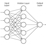
It might seem surprising then that we don’t really have a deep understanding of how deep learning works. I’m not talking about what you might call a mechanical understanding of neural nets; that we have down pretty well and we continue to improve through more hidden layers and techniques like sharpening and pooling. We understand how layers recognize features and how together these ultimately lead to recognition of objects. But we don’t have a good understanding of how recognition evolves in training and why ultimately it works as well as it does.

On reflection, this should not be surprising. Whenever technology advances rapidly, theory lags behind and catches up only as technology advances moderate. Some might wonder why we even need theory. We need it because all sustainable major advances eventually need a solid basis of theory if they are to have predictive power. Without that power, figuring out how to build even better solutions and knowing where the limits lie would all depend on trial and error, quickly becoming prohibitively expensive and undependable. Theoretical predictions still have to be tested (and adjusted) in practice but at least you know where to start.

Naftali Tishby of the Hebrew University of Jerusalem has developed an information theory of deep learning as a contribution to this domain, which seems like a pretty reasonable place to start. He makes the point that classical information theory is concerned only with accurate communication without an understanding of the semantics of what is communicated, whereas deep learning is all about the semantics (is this a dog or not a dog?). So an effective theory for deep learning, while following somewhat similar lines to Shannon’s theory, needs to look at loss of “relevant” information rather than loss of any information.

The theory details get quite technical, but what is more immediately accessible are implications for how deep learning evolves, especially as exposed by this team’s work in studying many training experiments on a variety of networks. They mapped the current state of their information metric by planes in a network and looked at how this evolves by epoch (a complete pass through the training data; multiple passes are typically made until error rate is acceptable). Before the first epoch there is high information in the first (labeled) layer and very little in final layers.

As epochs proceed, information with respect to labelling rises rapidly by layer (fitting), until this reaches a transition. At this transition, the network has minimized error in classifying the training examples seen so far, but the interesting part happens in subsequent training. Here detection accuracy does not improve but the number of bits in their input information metric (by plane) begin to drop. Tishby calls this compression; in effect, layers in the network are starting to drop information which is not relevant to the recognition problem. Put another way, during this phase, the network is learning to generalize, ignoring features in training examples which are not relevant to the object of interest.

The theory promises value not only in understanding this evolution but also being able to quantify the value of hidden layers in accelerating the compression phase, also bounds on accuracy, both of which are important in understanding how far this technique can be pushed and into what domains.

This is obviously not the last word on theory for deep learning (explaining unsupervised learning, for example) but is seems like an interesting start. A number of other researchers of note find this work at minimum intriguing and quite possibly an important breakthrough. Others are not so sure. In any case, it is by efforts like this that deeper understanding progresses, and we can certainly use more of that in this field. You can read more on this topic in this Wired article.


Qualcomm’s New Spectra ISP and Camera Modules Enable Nextgen AR

Qualcomm’s New Spectra ISP and Camera Modules Enable Nextgen AR
by Patrick Moorhead on 01-03-2018 at 12:00 pm

The mobile VR and AR space has been evolving rapidly, with many different players innovating in recent months. Companies like Apple and Google have been innovating on the software and hardware front, but others have been working diligently to support some of these efforts as well. One of those companies is Qualcomm with their support of technologies like Google’s Tango platform. However, Tango has had some challenges in taking off with the complexity of the hardware requirements proving to be a challenge for OEMs to ship in volumes.

In the past, Qualcomm had a camera module program co-branded with their ISP (image signal processor) which processes the image data from the cameras. This program was designed to make it easier for Qualcomm’s customers, the smartphone OEMs to quickly and reliably implement dual camera setups with a wide angle and telescopic zoom camera. That was what the market needed in the past, but now the market needs new capabilities which Qualcomm’s new Spectra Module Program and ISP will support.

The new Spectra Camera modules include an Iris Authentication Module that has latency as low as 40ms and features an Omnivision 1080P IR sensor for high resolution iris image capture. The real focus with these new camera modules, however, comes from the computer vision capabilities which include both passive and active depth sensing capabilities. The entry-level solution for value-tier devices will feature two cameras and passively calculate depth, allowing for more coarse measuring and lower cost. The high-end active depth sensing camera solution will feature three cameras including an IR emitter and IR camera for high resolution depth sensing at distances up to 4 meters and 0.1 mm accuracy.

The Spectra Camera modules and some of their capabilities will be supported by the newest generation of Spectra ISP inside of the next generation Snapdragon SoC. This new ISP will support features like multi-frame noise reduction in hardware which is like what Google already does in software with their HDR+ algorithm and make it available to anyone that uses their ISP. Qualcomm’s new Spectra ISP also supports motion compensated temporal filtering (MCTF) and accelerated EIS (electronic image stabilization) which cleans up the noise in low-light video and helps to sharpen the image as well, making low light video quality significantly better. Last but certainly not least is the implementation and support for 6-DoF and SLAM with 16ms motion to photon latency for inside-out tracking at room scale and collision avoidance. This paired with the new Spectra Camera module will enable highly precise AR solutions that can rely on the sub-mm accuracy point cloud generated by the Spectra Camera module and Spectra ISP inside of the Snapdragon.

Qualcomm’s new camera modules, especially their active depth sensing camera module, seem like no-brainers for Android OEMs to adopt to compete with what many expect that Apple will implement in the new iPhone 8. Qualcomm’s new ISP features are also sure to elevate the camera experience for Android smartphone users and can help to rise the tide that lifts all boats. Right now, the more integrated and simple an AR solution, the more likely OEMs and developers are to pick it up and build towards it. I believe that this new camera module helps to bring the Android ecosystem closer to where we expect Apple will be with the iPhone 8.


Semiconductor Devices Transforming the World

Semiconductor Devices Transforming the World
by Daniel Nenni on 01-03-2018 at 7:00 am

As we begin another new year we begin another semiconductor conference cycle starting with SEMI ISS on January 15–18 at the Ritz-Carlton in Half Moon Bay California. This conference really sets the tone for the year and gives us a place to start thinking, acting, and reacting. This year it is all about the electronic devices we have all been working on and hearing about that will change the world, hopefully.

Smart, Intuitive & Connected: Semiconductor Devices Transforming the World
Something transformative is happening in electronics, taking many forms, shapes, and sizes. From stunning, 360-degree visions powered by augmented reality and intuitive behavior propelled by artificial intelligence, to perceptual computing within intelligent vehicles. Deep learning in robotics, the sleek functionality of smartphones, and the limitless connectivity within cloud — one variable resides at the core of so much innovation: the semiconductor silicon)

Through collaboration across an expanding ecosystem, our industry is delivering supremely sophisticated semiconductor devices, enabling the transformation of our world into a place where lifestyle and efficiency are optimized in ways never imagined. Indeed, through innovations in equipment, materials, design, and packaging, emerging application trends within electronics incorporate essential features that defy convention, including higher performance, less power consumption, smaller footprint, and heterogeneously integrated components.

To succeed in a transformational marketplace, shrewd business decisions are more critical than ever. Dynamic application markets, competitive product segments, and unprecedented industry consolidation make time-to-market a make-or-break proposition. ISS 2018 will explore strategy, discuss collaboration, examine threats, and expound upon the market opportunities empowered by today’s semiconductor technologies.

This year’s speakers come from a wide range of companies including our own Scott Jones of IC Knowledge. As you know Scott is the gold standard on process technology coverage here on SemiWiki.com. Scott is speaking on day 2 at 9:00 am on “The Impact of EUV on the Semiconductor Supply Chain”. Do not judge Scott by his picture on the SEMI site :rolleyes:. Scott is very approachable, a straight shooter, and will not dodge your questions, absolutely.

The other speaker companies include:

  • Accenture
  • Alpha Capital Partners
  • Amazon Web Services
  • ASE
  • ASML
  • BCA Research
  • Gartner
  • IBM
  • IC Knowledge
  • IHS Markit
  • Imec
  • Intel
  • Integrated Sensing Systems
  • McKinsey & Company
  • Mentor Graphics, a Siemens Business
  • Nissan Research Center Silicon Valley
  • Oculus
  • SEMI
  • Tufts University
  • Versum Materials

You can see the full agenda HERE.

The other must see presentation is “Predicting the Next Wave of Semiconductor Growth” by Dr. Walden Rhines President, and CEO of Mentor, a Seimens Business. Wally has his finger on the semiconductor pulse like no other and speaks from the heart and mind.

I will also be at the ISS CxO Panel “Nodes, Inter-nodes, and Real Nodesjust for the fun of it! Seriously, this should be one of the funniest panels ever:

A node is a node is a node could have once been considered a law of identity statement for semiconductor technology. Indeed, the term ‘node’ was invented to be a yardstick of accountability at its most basic level. On the one hand, it’s been distorted by marketing. On the other, Moore’s Law can’t keep up with the annual alarm clock set to the law that Christmas can’t be moved. This has led to internodes, as simple design revisions are no longer enough to have competitive products in the hotly contested holiday sales cycle. This panel brings together some of the world’s sharpest minds to untangle these issues and shed light on what the real nodes are.

Comparing IDM and foundry process nodes has been entertaining over the years but now that the foundries have caught up it is somewhat sad to see Intel trying to redefine leadership to their advantage, my opinion. I am interested to see what panelists John Chen, Ph.D. V.P. of Technology and Foundry Management, Nvidia and Antun Domic, Ph.D., Chief Technology Officer, Synopsys have to say. They are fabless experts and should have no problem cutting through the nonsense. Scott Jones has already covered this in detail: Intel Manufacturing Day: Nodes must die, but Moore’s Law lives! and 14nm 16nm 10nm and 7nm – What we know now which was widely read (more than 150,000 views) and commented on. Let’s see if this panel discussion is blog worthy…

I hope to see you there!

Also Read: 2017 in Review and 2018 Forecast!


Cryptocurrency is the New Target for Cybercriminals

Cryptocurrency is the New Target for Cybercriminals
by Matthew Rosenquist on 01-02-2018 at 12:00 pm

As predicted, the rise of cryptocurrency valuation has captured the attention of cybercriminals. New hacks, thefts, misuse, and fraud schemes are on the rise. Where there is value, there will be a proportional risk of theft.Criminals always pursue and exploit systems where they can achieve personal financial gain. It is the Willie Sutton effect: That’s where the money is.
Continue reading “Cryptocurrency is the New Target for Cybercriminals”


What’s old is new again – Analog Computing

What’s old is new again – Analog Computing
by Bernard Murphy on 01-02-2018 at 7:00 am

Once in a while I like to write on a fun, off-beat topic. My muse today is analog computing, a domain that some of us antiques in the industry recall with fondness, though sadly in my case without hands-on experience. Analog computers exploit the continuous nature of analog signals together with a variety of transforms to represent operations to solve real-value problems. In the early days, certain problems of this type were beyond the capabilities of digital computers, a notable example being finding solutions for differential equations. If you have taken a basic analog design course, you already know of an important transform relevant to this domain; an op-amp with a capacitative feedback loop acts as an integrator.


Coming out of the Second World War and moving onto the Cold War, Korea, Vietnam and other potential and real engagements, there was high interest in improving accuracy in firing control. This required solving, guess what, lots of differential equations defined by the mechanics of projectiles (thrust, gravity, air resistance, et al). Analog computing became hot in defense and aerospace and remained that way until digital (and later DSP) techniques caught up and surpassed these systems. Even the general public could get in on the action. Heathkit (another name from the past) sold a hobbyist system as early as 1960, long before most of us were thinking of digital computers.

But that was then. Are analog computers now just an obscure footnote in the history of computing? Apparently not. One hint was an article appearing recently in IEEE Spectrum. A team at Columbia University has been building integrated analog computers, where connectivity between analog components is controlled digitally. They are now on their third-generation chip.

These computers can solve problems (within their scope) within the order of a millisecond, though the solutions are accurate only to within a few percent, thanks to noise. The Columbia team view this as a good way to provide an approximate solution as input to a digital solver which can finish the job. Since finding an approximate solution is often the hardest part of solving / optimizing, the hybrid combination of analog and digital could be quite valuable. That said, there are plenty of challenges to overcome. One example is bounded connectivity in a 2-dimensional implementation. Functions can easily be constructed between neighboring components but connecting to other more distant functionality is generally fraught with problems for analog signals. Still, you could imagine that solutions might be found to this problem.

A more interesting (for me) possibility for analog/mixed-signal systems is around neuromorphic computing. What we are most familiar with in neural modeling is neural nets (NN) used for recognition applications, modeled using GPUs or DSPs or specialized hardware. But neural nets such as these are very simple models of how neurons really work. Real neurons are analog so any model has to mimic analog behavior at some level of accuracy (which is why DSPs are so good at this job). However, neuron behavior is more complex than the basic NN model (sum inputs, apply a threshold function, generate an output). For example, some inputs may reinforce or suppress other inputs (sharpening, which is related to remembering and forgetting).

More generally, inputs to a real neuron are not undifferentiated connections. Output(s) from a neuron to other neurons can be mediated by any one of multiple possible neurotransmitters with different functions, including the sharpening functions mentioned above. And all of this can be bathed in hormones secreted from various glands which further modulate the behavior of neurons. Who cares, you say? If one goal in building intelligent systems is to more closely mimic the behavior of the brain, then stopping at present day neural nets seems to be throwing in the towel rather too quickly, given real neuron complexity.

Which is why the Human Brain Project in Europe and the BRAIN Initiative in the US are working to jointly advance neuroscience and related computing. This has driven quite a bit of development in neuromorphic compute systems, such as the Neurogrid developed at Stanford. What is especially interesting about many of these systems is the significant use they make of analog computation together with digital methods. Here, differential equations play no part (as far as I know). The motivation seems much more around low-power operation (Stanford cite a 10[SUP]5[/SUP] reduction in power over an equivalent supercomputer implementation) and a tolerance to analog noise-related inaccuracies in this application. After all, real neurons aren’t hyper-accurate and NN implementations for inferencing are already talking about 1- or 2-bit accuracy being sufficient for image recognition.

The constraints faced by the Columbia work don’t play such a big role here. In using analog to model neuron behaviors, 2D bounds on a chip reflect physical bounds in the brain (and if you need to go 3D, presumably that would be possible too with stacking). So maybe the big comeback for analog computing will be as a close partner with digital in neuromorphic computing. Perhaps someday this approach may even replace neural nets?


IBM Plays With The AI Giants With New, Scalable And Distributed Deep Learning Software

IBM Plays With The AI Giants With New, Scalable And Distributed Deep Learning Software
by Patrick Moorhead on 01-01-2018 at 11:00 am

I’ve been following IBM’s AI efforts with interest for a quite a while now. In my opinion, the company jump-started the current cycle of AI with the introduction of Watson back in the 2000s and has steadily been ramping up its efforts since then. Most recently, I wrote about the launch of PowerAI, IBM’s software toolkit solution to use with OpenPOWER systems for enterprises who don’t want to develop their AI solutions entirely from scratch but still want to be able to customize to fit their specific deep learning needs. Today, IBM Research announced a new breakthrough that will only serve to further enhance PowerAI and its other AI offerings—a groundbreaking Distributed Deep Learning (DDL) software, which is one of the biggest announcements I’ve tracked in this space for the past six months.

Getting rid of the single-node bottleneck

Anyone who has been paying attention knows that deep learning has really taken off in the last several years. It’s powering hundreds of applications, in consumer as well as business realms, and continues to grow. One of the biggest problems holding back the further proliferation of deep learning, however, is the issue of scalability. Most AI servers today are just one single system, not multiple systems combined. The most popular open-source deep learning software frameworks simply don’t perform well across multiple servers, creating a time-consuming bottleneck. In other words, while many data scientists have access to servers with four to eight GPUs, they can’t take advantage of it and scale beyond the single node—at the end of the day, the software just wasn’t designed for it.

Enter the IBM DDL library: a library built with IBM Research’s unique clustering methods, that links into leading open-source AI frameworks (such as TensorFlow, Caffee, Torch, and Chainer). With DDL, these frameworks can be scaled to tens of IBM servers, taking advantage of hundreds of GPUs—a night and day difference from the old model of doing things. To paint a picture, when IBM initially tried to train a model with the ImageNet-22K data set, using a ResNet-101 model, it took 16 days on a single Power “Minsky” server, using four NVIDIA P100 GPU accelerators. A 16-day training run means a significant delay of time to insight, and can seriously hinder productivity.

IBM is calling DDL “the jet engine of deep learning”—a catchy moniker that honestly isn’t too far off the mark in my opinion. Using DDL techniques, IBM says it was able to cut down that same process to a mere 7 hours, on 64 Power “Minsky” servers, with a total of 256 NVIDIA P100 GPU accelerators. Let me reiterate that: 16 days, down to 7 hours. If these results are accurate, which I think they are, it’s clear why IBM thinks it has a real game-changer on its hands. IBM’s new image recognition record of 33.8% accuracy in 7 hours handily surpasses the previous industry record set by Microsoft—29.9% accuracy in 10 days. To top it all off, IBM says DDL scales efficiently—across up to 256 GPUs, with up to 95% efficiency on the Caffe deep learning framework.

Now available in beta

Developers won’t have to wait to try out this new technology. IBM research is delivering a beta version of the DDL to IBM Systems, which is available now in the newly announced 4th revision of IBM’s PowerAI (for TensorFlow and Caffe, with Torch and Chainer to follow soon). I think this will be a great addition to IBM’s Power systems, which I’ve called the “Swiss Army knives of acceleration”—standard PCI express, CAPI, and NVLink, all wrapped up in one platform.

Another unique thing of note about DDL is that it will be available not only on-prem but also through the cloud—via a cloud provider called Nimbix. In today’s hybrid environment, this flexibility is obviously a plus. Developers can try it out beta version now on Nimbix, or on an IBM Power Systems server.
Wrapping up

One of the most interesting things for me is that this new technology is coming from IBM, not one of the flashier, louder AI proponents like Google or Facebook. It looks like if IBM can continue to bring “firsts” to the table, IBM is really shaping up to be not just a major player in the enterprise, but for deep learning overall. DDL and OpenPOWER are the secret sauce that I think will give IBM an edge it needs—significantly cutting down training times, and improving accuracy and efficiency. I’ll continue to watch with interest, but I think by getting rid of this bottleneck, DDL has the potential to really open the deep learning floodgates. It could be a real game-changer for IBM, PowerAI, and OpenPOWER.


HDMI 2.1 Delivers 48.0 Gbps & Supports Dynamic HDR

HDMI 2.1 Delivers 48.0 Gbps & Supports Dynamic HDR
by Eric Esteve on 01-01-2018 at 7:00 am

You may or may not have bought HDMI-equipped device for black Friday or during year end break, but you TV set (or/and you PC) are certainly HDMI-powered, like the 750 million HDMI-equipped devices sold in 2016. In fact, cumulated shipment of HDMI-equipped devices has reached 6 BILLION since the protocol introduction in 2003! HDMI 1.0 was delivering 4.5 Gbps, enough to support 1080p standard, and HDMI 2.1 delivers more than 10x with 48 Gbps. We have to remember that HDMI protocol is unidirectional, unlike USB or PCI Express, and the function is built by using four PHY, each delivering 12 Gbps.


What about HDMI competition? We can forget about Diiva, born in the early 2010’s (and disappearing just a couple of years later). DisplayPort, launched by VESA in 2006 could be seen as a direct competitor at that time, but HDMI was supported by much stronger marketing from Silicon Image and HDMI Licensing LLC (founded by Hitachi, Panasonic, Philips, Silicon Image, Sony, Thomson (RCA) and Toshiba). DisplayPort protocol is now mostly used to connect a computer monitor to a PC, but is not active in the consumer TV segment.

You may have heard about ThunderBolt (and if you use it you are more likely an Apple customer!). The protocol is not point to point like HDMI, but daisy chained: a single Thunderbolt port can support up to six Thunderbolt devices. Looks smart, but ThunderBolt penetration was penalized by higher price, as only high-end devices were equipped, and also by the lack of available IP as Intel didn’t want to license the technology as a design IP… This was not the case with HDMI and we can see that HDMI Licensing strategy, more open compared with ThunderBolt, has allowed this huge market penetration: HDMI is now ubiquitous in the consumer/computer segments when TV is concerned.


As we mention IP, it’s interesting to notice the market evolution for HDMI protocol. If Silicon Image has been the undisputed leader for years since HDMI introduction, for ASSP as well as for IP sales, their IP sales went down dramatically, the IP group was sold to Lattice who eventually sold it to Invecas. And, like for most of the protocol based interface IP, Synopsys is now the clear leader, as you can see on the above figure from IPnest that Synopsys includes in their HDMI pitch (which make me proud…).

In fact, the strongest Synopsys competitor is made of internal design teams developing their own HDMI IP. It was probably not so difficult to design 1.5 Gbps SerDes for HDMI 1.0, but the last protocol release, HDMI 2.1, has to deliver 48 Gbps over 4 PHY. The solution requires using 12 Gbps SerDes to deliver 48 Gbps aggregate bandwidth for uncompressed 8K resolution at 60 Hz refresh rate. But the speed is only one part of the equation as the HDMI 2.1 solution from Synopsys also supports new Dynamic HDR, eARC, VESA DSC 1.2a and HDCP 2.2.


If we compare HDMI 2.1 with DisplayPort 1.4, both are supporting 8K video, but the difference is that HDMI allow supporting uncompressed 8K. High Dynamic Range (HDR) feature is also known as Dolby Vision and has been implemented in HDMI 2.0a (released on April 8, 2015) and DisplayPort 1.4 (released on March 1, 2016). With HDMI 2.1 standard, released on January 2017, Hybrid Log-Gamma (HLG) support had been added to the HDMI 2.0b standard, allowing now to claim Dynamic HDR support. Dynamic HDR is dynamic metadata that allows for changes on a scene-by-scene or frame-by-frame basis.

Because most of the TVs are used with soundbars, it was important to make life easier for customers, and that’s one of the goals of eARC, as it simplifies connectivity and discovery between TVs and soundbars. eARC also supports most advance audio formats and highest audio quality.

To provide smoother, lag-free and more fluid gaming experience, Synopsys has implemented Enhanced Refresh Rates: Variable Refresh Rates (VRR), Quick Media Switching (QMS), Quick frame Transport (QFT) or Auto Low Latency Mode (ALLM).

No doubt that your next TV set will be HDMI 2.1-equipped!

By Eric Esteve from IPnest


2017 in Review and 2018 Forecast

2017 in Review and 2018 Forecast
by Daniel Nenni on 12-30-2017 at 7:00 am

This has been an amazing year for me both personally and professionally. Personally we are now empty nest and have our first grandchild. SemiWiki is prospering, a company that I have been involved with for ten years (Solido Design) had a very nice exit, and my time promoting semiconductor stocks to Wall Street paid off with the PHLX Semiconductor index (SOX) gaining an astounding 40%.
Continue reading “2017 in Review and 2018 Forecast”