Banner Electrical Verification The invisible bottleneck in IC design updated 1

Why It’s A Good Idea to Embed PVT Monitoring IP in SoCs

Why It’s A Good Idea to Embed PVT Monitoring IP in SoCs
by Daniel Payne on 02-16-2018 at 7:00 am

At Intel back in the late 1970’s we wanted to know what process corner each DRAM chip and wafer was trending at so we included a handful of test transistors in the scribe lines between the active die. Having test transistors meant that we could do a quick electrical test at wafer probe time to measure the P and N channel transistor characteristics, providing valuable insight for the specific processing corner. We would’ve loved to have this kind of test transistor data for processing embedded into each die as well. The increase in transistor complexity for DRAM chips has been quite dramatic over the years, so in 1978 we had 16Kb DRAM capacity while today the technology has reached 16Gb, an increase of 1,000,000X. On the SoC side we see an equally impressive increase such that a GPU from NVIDIA now contains 21 billion transistors and 5,120 cores using a 12nm process from TSMC. So whether you are designing a CPU, GPU, SoC or a chip for IoT applications requires that IC designers understand how process variability impacts each die and packaged part during operation. Other design concerns include:

  • Manufacturability and yield
  • Timing, clock speed, power values within spec
  • Reliability effect like aging, internal voltage drop
  • Avoiding field failures

Moore’s Law has held up pretty well until the 28nm node, and below that node the price learning curve hasn’t been as rewarding. Even clock speeds have stalled in the GHz range. Short-channel effects started to hurt current leakage values, limiting battery life and performance, so new transistor approaches emerged like FinFET and SOI. Device variability is a dominant design issue today, meaning that even adjacent transistors on the same die can have different Vt (Voltage Threshold) values caused by different dopant values or silicon stress caused by proximity to isolation wells – layout dependent effects. Just take a look at how variations have increased with each smaller geometry node from 90nm down to 22nm:


Switching speed delay variations against supply voltage across process nodes (Source: Moortec)

For a 22nm process node with a 475mV supply level you can expect switching speed delay variations of 25%, while at the more mature process node of 90nm the delay variations are only 9%.

With FinFET technology in use since 22nm there are some new concerns caused by higher current densities like localized heating effects, so designers using 14nm, 10nm, 7nm and 5nm need to be aware of self-heating because it impacts the aging of transistors and the Vt actually begins to shift over time as shown below:


Vth degradation from NBTI and HCI effects (Source: Moortec)

The dark curve above shows a Vdd value of 1.3V being used for transistors, and over a 10 year operating period the nominal Vt value of 0.2V can be changed by over 4% due to negative bias temperature instability (NBTI) and hot carrier injection (HCI) effects. That Vt shift can simply slow down your IC or cause it to fail meeting your clock speed specification.

With lower Vdd values being used coupled with higher current levels and higher interconnect resistivity you can expect to see internal supply levels of a chip drooping from the values supplied at the pins. Knowing the actual internal Vdd levels can be quite critical.

To meet stringent power consumption requirements many approaches have been taken, a popular technique is called Dynamic Voltage and Frequency Scaling (DVFS) where the chip has the ability to change local Vdd values in order to throttle or speed up the frequency of operation. Reducing the Vdd value quickly reduces power consumption because power is related the square of the Vdd value. So lowering the Vdd value locally allows you to tune for power consumption. Adding DVFS does increase the logic overhead and requires even more simulation during the design phase. Turning local Vdd lines on causes a rush of current, triggering an IR drop issue which can cause transient errors in the silicon logic behavior.

IC designers can deal with all of these effects by a couple of approaches, the earliest approach was to design for worst-case conditions although at the expense of leaving margin on the table. A newer approach is to actually embed in each chip some specialized IP for three tasks:

  • Temperature sensing
  • Voltage monitoring
  • Process monitoring

Knowing your actual PVT (Process, Voltage, Temperature) corner in silicon is incredibly useful to controlling your chip for maximum performance. With an embedded PVT monitor you can quickly perform speed binning without having to run extensive functional, full-chip testing. Aging effects on Vt can be measured with an embedded PVT methodology.

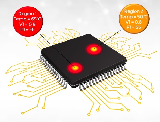
Using a temperature sensor at strategic locations on an SoC can then be used to dynamically measure how hot each region is, then decide to alter the Vdd values to keep the chip operating reliably while still meeting timing, even as the chip ages over time. A multi-core SoC with temperature sensors can dynamically assign new instructions to the core with the lowest temperature value, balancing the work load so as to not over-heat any one core with too many sustained operations. The mean time to failure for ICs is directly related to operating temperature levels, so with embedded PVT you can control the aging effects.

Moortec is the IP vendor that designed PVT monitoring for popular process nodes and they have internally created the sensors and controllers to interpret the data on-chip. Yes, you have to use a tiny amount of silicon area to implement the PVT monitoring, however the benefits far outweigh the die size impact. The process monitor can tell you the exact speed of your transistors to let you know how close they are to nominal values. Benefits of using these monitors include:

  • Tuning on-chip parameters at product test
  • Real-time managements of processor cores
  • Avoiding localized aging effects
  • Maximizing clock performance at a specific voltage and temperature

You can use PVT monitors to measure if your specific silicon will meet timing goals, or program local Vdd levels to achieve a certain clock speed. It also can make sense to have multiple PVT monitors spread out across a single die in order to collect regional data. For example you could place a PVT monitor in each corner of a die, then one in the center in order to measure process variability. For multi-core SoCs you would place PVT monitors in each core, next to critical blocks.

Engineers at Moortec have designed PVT monitors across a wide range of process nodes starting at 40nm and extending through 7nm, so you don’t need to be a PVT expert to use their IP. You get to consult with their experts about which PVT monitors to use and where to place them on your specific chip design. To really get the most performance out of advanced FinFET nodes you should consider adding PVT monitors into your next design, even the battery-powered IoT designs benefit from the data gathered by PVT monitors in saving power consumption.

There’s an 11 page white paper available at Moortec for download after a brief sign-up process.


SPI Inspires a New Generation of SOC Designs

SPI Inspires a New Generation of SOC Designs
by admin on 02-15-2018 at 12:00 pm

When I started dabbling in hardware again for fun using Arduinos about five years ago, it had been a long time since I had played with microprocessor chips. The epiphany for me was seeing how easy it was to load programs onto the onboard flash on something like an Atmel AVR using the SPI interface. My previous experience decades early brought up visions of bulky parallel interfaces with complicated programming units. The USB to SPI interface was essentially one chip and a few discretes. I also played with the SPI, in its most basic form, to drive programmable LED strips. Of course, SPI has mushroomed into a popular and essential interface for many embedded and SOC based systems. I was therefore pleased to see a webinar by Silvaco that delved into SPI and its many applications today.

The webinar, cleverly named SPI vs SPI, aired recently, but is now available for viewing on the Silvaco website. For those who are missing the SPI vs SPI reference, look up Mad Magazine, another one of my childhood favorites. With Silvaco’s acquisition of IP Extreme, they have become a significant player in the IP market. The webinar was hosted by Jim Bruister, Director of Digital Systems at Silvaco. MCU programming aside, the main application for SPI is the broader field of flash memory enabled devices. These cover a large range of consumer, IoT and networked products.

External flash memory for these products is enabled by SPI and helps solve many system and SOC level problems. Nonvolatile memory is needed for storing boot images and startup. However, onboard flash can be a problem due to cost or process compatibility. Rather than have embedded flash availability dictate SOC process selection, off-chip flash decouples the choices.

Even though SPI started out as a single data line serial interface, it has increased in speed and added bus width to boost performance. It has evolved from 1 bit at 1MHz to up to 8 bits running at 200MHz. At the same time is has preserved its simple and effective clocking and bus arbitration scheme. Jim pointed out during the presentation that with the newer SPI IP, a serial SPI bus running at 80MHz can exceed the throughput of a 32 bit parallel bus with a 90ns access time. At the same time SPI requires one 8 PDFN part, and the parallel interface would need 2 of the 64 BGA parts and the 64 traces that go with them.

Silvaco has IP for Quad and Octal SPI controllers. These interface with a large number of commercial flash memories and integrate inside SOC’s with ARM’s AMBA AHB and AXI interfaces. The story really gets interesting when Execute in Place (XIP) comes into the picture. XIP allows for external flash to be used as if it were system memory. This vastly expands system architecture choices. With XIP there is DMA support, which can be used to load encrypted images from external flash devices for increased security.

Jim’s talk articulates several scenarios where XIP, DMA and other advanced features of their high-performance SPI IP are used. Jim also discusses the software support available for system operation and debug. Silvaco offers a QSPI Boot Loader that copies external boot code stored on flash memory into internal SRAM and then re-boots. They also have a QSPI flash loader that is useful copying data to flash memory chips.
SPI is one of those long running success stories, from its origins in the 1990’s it has evolved and become newly important to an entire class of SOC based designs. With quad and octal designs running at high speeds, it has kept pace with data and throughput requirements. SPI enables data transfers with vastly fewer traces and with smaller and less expensive packages. SPI IP is an ideal example of how system level IP can help improve customers’ time to market, lower expenses and increase predictability. The webinar which is online now describes in more detail how a variety of solutions can be designed to incorporate flash memory by using Silvaco SPI IP.


Webinar: Bottlenecks be Gone – Automated Performance Verification with Synopsys

Webinar: Bottlenecks be Gone – Automated Performance Verification with Synopsys
by Bernard Murphy on 02-14-2018 at 10:00 pm

Performance verification is among the most challenging of objectives in any SoC verification plan. It’s difficult to start effectively until quite late in the development cycle, at which point you don’t have a lot of time left to develop extensive performance-oriented testbenches. So many teams adapt functional tests to this purpose, typically a less than ideal way to truly stress performance. Even then they must comb through log and other files to extract latencies, bandwidths and other performance-related metrics, then compare these with targets.

Vaishnav Gorur, product marketing manager in the verification group at Synopsys, told me this has been a common concern he has heard from multiple verification teams and architects. This encouraged Synopsys to develop more automation around performance testing in their just-released VC VIP AutoPerformance and Verdi Performance Analyzer products. This tool automates the construction of traffic stimulus, orchestrating runtime traffic, visualizing and analyzing metrics, automating checking (did I meet targets) and diagnostic traceback (show me the packets that led to this problem).

From what I can see, there are four main components to a performance verification solution in this flow solution:
• VC AutoTestbench for building the testbench
• VIP for Arm® AMBA® protocol
• VC VIP AutoPerformance automates building the performance test from a test
• Extensive support within Verdi for performance-related metrics: latencies, bandwidths, counts, user metrics, all with user-definable thresholds, protocol-aware transaction tracking, linkages between violations and transactions, linkages to signals, memory activity/value tracking, cache operation/history tracking, you get the idea.

Synopsys has been making a big push to simplify and accelerate SoC verification. I recently introduced their webinar on automating building the SoC testbench, reducing time from a standing start to “lights-on” from days/weeks to hours. This webinar provides and overview on the solutions they are releasing targeting this objective.

You can register HERE for this webinar on February 21st at 10am PST

Abstract
Performance is a critical source of competitive advantage for modern SoCs, and performance targets need to be verified on top of functionality. SoCs can be configured in a multitude of ways with different IP and interconnect topologies, number of masters and slaves, bus widths, packet sizes, clock speeds, etc., and performance verification can quickly get overwhelming. Further, given SoC performance verification is often done towards the end of the project cycle, there is a pressing need for push-button performance verification, analysis and debug.

In this Synopsys webinar, we will outline an automated flow to perform end-to-end performance verification using Synopsys VC VIP AutoPerformance, Verdi Performance Analyzer and Verdi Protocol Analyzer. We will also include a demo of this flow using a real-world design and Synopsys VIP for Arm® AMBA® protocol.

Specifically, you will learn:
• How to quickly create a test profile for VC VIP AutoPerformance to auto-generate stimulus for performance testing
• How to easily preset thresholds for key metrics such as latency, bandwidth etc. to auto-detect performance bottlenecks
• How to analyze and seamlessly debug performance issues right down to the violating transaction


Vaishnav Gorur
Product Marketing Manager
Verification Group, Synopsys

Vaishnav Gorur is currently Staff Product Marketing Manager for Debug & SoC Verification Automation products in the Verification Group at Synopsys. He has over 12 years of experience in the semiconductor and EDA industry, with roles spanning IC Design, field applications, technical sales and marketing. Prior to joining Synopsys, Vaishnav worked at Silicon Graphics, MIPS Technologies and Real Intent. He has a Masters degree in Computer Engineering from University of Wisconsin, Madison and an M.B.A. from University of California, Berkeley.


Satyapriya Acharya
Senior Manager – Applications Engineering
Verification Group, Synopsys

Satyapriya Acharya is a Senior AE Manager at Synopsys, where he manages the use of Synopsys Verification IP for ARM AMBA protocols with several key customers. He has been involved in the development, verification, and deployment of Synopsys Verification IP for the AMBA 3, AMBA 4 and AMBA 5 specifications. He has over 15 years of experience in design and verification.


Data Security – Why It Might Matter to Design and EDA

Data Security – Why It Might Matter to Design and EDA
by Alex Tan on 02-14-2018 at 12:00 pm


According to the Economist,
The world’s most valuable resource is no longer oil, but data”.
Is this the case?Data is the by-product ofmany aspects of recent technology dynamics and is becoming the currency of today’s digital economy. All categories in Gartner’s Top10 Strategic Technology Trends for 2018 (Figure 1) imply the generation, handling and processing of massive amount of data.

On May 25, 2018, the European Union (EU) plans to enact GDPR (General Data Protection Rules) aiming to streamline data privacy laws across Europe and to reshape the way organizations across the region approach data privacy/protection. The regulation biggest change is related to extending the jurisdiction of the GDPR (territorial scope applicability), as it will apply to all companies processing the personal data of data subjects residing in the EU, regardless of the company’s location.

Should we care about data security and protection? Does it have anything todo with design or EDA communities? There are several major reasons we should. Let’s take a look on three aspects:

First, the financial consequence to the business operation for failing to protect or properly handling sensitive data could be detrimental.Breaching GDPR can result in fines ranging from 2% for minor violations (e.g.disorderly recordkeeping) and up to4% of company worldwide revenue or €20 Million (whichever is greater). Such a hefty fine can be imposed for the most serious infringement, e.g. for not having sufficient customer consent to process data or violating the core of Privacy by Design concepts. Hence, many cloud providers such as Amazon (AWS) and Microsoft (Azure) were the first group to embrace steps to prepare for this rule enforcement and have established guidelines to tackle customer data and complying with GDPR. Similar data privacy enforcement is also done in the US by the Federal Trade Commission (FTC), although by means of varying list of imposed rules such as The 1974 Privacy Act, the Fair Credit Reporting Act (for financial domain), the Electronic Communications Privacy Act (consumer proprietary network info).

Second,data has gained increased importance due to the advent of Artificial Intelligence. Machine learning has facilitated more efficient engineering optimization and enhanced business analytics of traditional big data. Today’s cloud computing, network and machine learning have enabled the use of real time data, to augment historical data during active learning to produce optimal results. The entire solution supply-chain will take part in handling the data and share the burden of its safeguarding during and after each access. Within the context of the cloud providers, hardware companies will work with both upstream and downstream vendors to deliver a safe and complete solution. Table-1 highlights approaches used by key hardware companies to protect data.


What about the EDA world? Currently only a few EDA vendors have fully addressed ML implementation.ANSYS integrated ML, cloud access, data mapping and visualization facilities for its array of analysis products such that users could plug-in any further customization on topof its SeaScape stack platform (Figure 2). Solido (now part of Siemen) embedded ML into its characterization product but designated Solido Lab as facility to further collaborate with users. Both examples show approaches that accommodate users data proprietary nature. On the other hand, Cadence and Synopsys designplatforms have many underlying point tools such as synthesis,placement, routing, timing. Some of them had been augmented with ML flavors. However, boundaries introduced by these tools prompt unnecessary needs of frequent correlations, design margining and at times view-format transformations. While both vendors have made headways in aligning the delay computation engines (Cadence Gigaplace engine, Synopsys In-Design approach) non-unified database formats still limit data-flow and hence, optimal optimization with ML. It also has not addressed how to collaborate with users when badly needed data are also proprietary.

Third, sprouting digital ecosystems has blurred the boundary of private,corporate versus public domain data. For example, therapeutic medicine involves the potential use of private data (patient, doctor), public domain (Central Disease Control, county health) or corporate (hospital, insurance).Personal data gathered over time carry enormous value. EU estimates the value of European citizens’ personal data could grow to nearly €1 trillion annually by 2020. Some IT security techniques can be applied to protect the privacy of the data itself (i.e., anonymization– to remove personally identifiable infowhere it is not needed; pseudonymization– to replace personally identifiable material with artificial id; encryptionto encode messages so only those authorized can read it), but may not be sufficient.

In summary, the current digital revolution has produced massive data, crossing many evolving digital ecosystems and requiring all data shareholders to take a role in properly and safely handling them. This vary from revamping a more unified, seamless database platform to the need of collaborations in establishing a more solid data segregation (such as data IP) or standard access protocols.


FPGA Prototyping Exposed

FPGA Prototyping Exposed
by Daniel Nenni on 02-14-2018 at 7:00 am

In case you missed it, the FPGA Prototyping for SoCs webinar happened last week. I did the opening ceremonies which I will run through briefly here or you can go straight to the replay HERE.


FPGA prototyping is one of the fastest growing market segments we track on SemiWiki which brings us to the topic at hand: FPGA Prototyping for SoCs presented by S2C. Founded in San Jose, California, S2C has been successfully delivering rapid prototyping solutions since 2003.

Joining me today is Richard Chang, Vice President of Engineering at S2C. Richard has a Masters degree in Electrical engineering from the University at Buffalo and more than 20 years experience designing chips, including two US patents.

FPGA prototyping is a method to create a prototype of an SoC, ASIC, or System for the purpose of logic verification as well as early software development. FPGA prototyping today is used in all different types of applications such as consumer electronics, communications, networking, IOT, data center, autonomous driving, and artificial intelligence. FPGA prototyping can run at or close to real system speed in the ranges of tens of MHz and thus able to boot OS, run applications, and find deeply embedded bugs – significantly shortening the design validation time. FPGA prototypes are also affordable and therefore a large number of systems can be deployed to increase test coverage, shorten design validation time, and reduce the project risk.

With the advancement of software tools available around FPGA prototyping, FPGA prototypes today can be used throughout most design stages. Many commercial FPGA prototypes can link with the simulation environment through a transaction link such as AXI bus. This allows designers to start prototyping their idea on FPGAs early in the design cycle with part of their designs and test benches still in C/C++. FPGA prototypes are also ideal for block level and IP level verification.

It’s always a good practice to make sure each of your design blocks work before you put them together. In addition, many IP blocks today come from 3[SUP]rd[/SUP] party vendors or different design groups in your company. Prototyping with FPGAs first allows you to understand the behavior of these IP blocks at the system-level, easing system integration.

The next step is naturally integrating the entire system on FPGA prototypes. It will usually involve 2 things: multiple FPGAs and daughter cards. Most SoC designs will easily require 2, 4 or an even larger number of FPGAs to fit, and thus requires partitioning the designs as well as doing pin-multiplexing between the FPGAs as usually the interconnects between FPGAs after partitions are much larger than the available physical pins. This process can now be easily managed by partition tools such as Player Pro from S2C. You would also need daughter cards to hook up to real systems such as cameras, displays, memories or network connections. So, the ideal FPGA prototyping system needs to have good I/O expansion capability and a large library of daughter cards.


Finally, FPGA prototypes are used for early software development before the real silicon is available. Again, this is possible because FPGA prototypes run at or close to the real system speed and they are cost-efficient. Here’s a quick summary of FPGA prototyping benefits:
[LIST=1]

  • FPGA Prototyping can run at tens to hundreds of MHz while simulations are in range of tens of Hz and emulation in the range of hundreds of KHz.
  • FPGA Prototyping is much faster and therefore enables software development while other technologies may require hours to boot just the SoC OS.
  • FPGA prototyping can hook up to real system targets such as video inputs and outputs, network traffic, and test equipment. Other technologies would need speed bridges or a virtual traffic generator which may add complexity and not mimic the real world environment.
  • FPGA prototyping systems are usually small and portable allowing testing in real world environments or you can even do customer demonstrations.
  • With all the benefits above, FPGA prototyping systems are meant to catch those really hard to find bugs that need lots of data and lots of runs.
  • Finally, the cost of FPGA prototyping is a small fraction of Emulation and therefore allows a large number of systems to be deployed for concurrent development thus shortening your product development schedule.Headquartered in San Jose, CA, S2C is a worldwide leader in providing both hardware and software solutions for FPGA prototyping. S2C has a team of more than 60 people that is dedicated to delivering FPGA prototyping solutions serving more than 400 customers worldwide over the past 15 years.
    The S2C Prodigy Complete Prototyping Platform consists of 6 key components which are illustrated here:
    [LIST=1]
  • Prodigy Logic Modules are the main FPGA boards and they come in different configurations: Single, Dual and Quad. Xilinx and Intel Altera FPGAs.
  • Prototype Ready IP are available through off-the-shelf daughter cards and S2C has more than 80 different types such as: USB, PCIe, Ethernet, HDMI, and different types of memories. Most daughter cards are shipped with test designs so you can ensure they work out-of-box.
  • ProtoBridge is an AXI transaction link over PCIe and allows FPGA prototypes to communicate with simulation environments in workstations.
  • PlayerPro provides runtime control of your FPGA prototyping hardware remotely as well as the partitioning of your designs.
  • The MDM Multi-Debug Module allows concurrent capture of waveforms from multiple FPGAs on an external memory for very deep debugging.
  • Finally, multiple Prodigy Logic Modules can be linked together (in different configurations) and can be hosted in a Cloud Cube chassis.”With that I will turn it over to Richard for a more detailed discussion on FPGA prototyping for Socs”Richard then goes into more detail of how you FPGA Prototype an SoC finishing with a video of an HDMI interface. The Q and A section was very good, here are the questions we had time for:
    [LIST=1]
  • How do people decide between Xilinx and Intel FPGAs for prototyping?
  • I am familiar with Xilinx FPGAs, if I switch to an Intel FPGA platform, will it be difficult to convert my design?
  • The PlayerPro software sounds interesting, what more can you tell me about it?
  • How many FPGAs can your Multi-Debug Module support concurrent capture of waveforms?
  • How fast can we really run our design using FPGA prototyping?
  • I have daughter cards based on FMC-HPC mezzanine interface. Can I connect them to S2C prototyping boards?
  • Do you any tools to support pre-loading data file into BRAM (block memory) and DDR3/DDR4 memory? And how fast are these – bandwidth?
  • Our legacy daughter cards have 3.3 and 5 volts. But I see that most modern FPGAs support up to 1.8V. Do you provide any voltage level shift capability?For more information check the REPLAY. You can also download our book Prototypical HERE.

Unexpected Help for Simulation from Machine Learning

Unexpected Help for Simulation from Machine Learning
by Tom Simon on 02-13-2018 at 12:00 pm

I attend a lot of events on machine learning and write about it regularly. However, I learned some exciting new information about machine learning in a very surprising place recently. Every year for the last few years I have attended the HSPICE SIG dinner hosted by Synopsys in Santa Clara. This event starts with a vendor fair featuring companies that have useful interfaces and integrations with HSPICE. After a mixer in the vendor fair area, there is a dinner and several talks pertinent to the HSPICE user community.

Usually there are interesting talks by Synopsys customers on how they used the features of HSPICE in their flow to solve a vexing design problem. However, this time Synopsys threw us a curve ball. The main thrust of the talks this year focused on applications for machine learning in EDA, and specifically around HSPICE related issues. Naturally, EDA is not the first thing one thinks of when machine learning is mentioned. Yet, more and more, machine learning is being applied to difficult problems in electronics design.

It’s important to point out that machine learning is as good at numerical problems as it is at visual problems. During a panel portion of the dinner event, Synopsys Scientist Dr. Mayukh Bhattacharya clearly laid out the ideal scenario for using machine learning for a numerical problem. He cited the very broad definition of machine learning as “using a set of observations to uncover an underlying process”. There are three must haves: a pattern exists, we cannot pin it down mathematically, and we have data. It should be evident that these three conditions are met in a lot of SPICE related design problems.

As a good example was the talk that evening by Chintan Shah, VLSI Engineer of from Nvidia, where he has been working on clock methodology and timing. It’s interesting to think that Nvidia, a leader in machine learning technology, is applying machine learning to their own design methodology. In particular Chintan use machine learning to predict clock cell joule self-heating in their designs. Self-heating has become a much bigger issue with the advent of FinFET devices. FinFET self-heating can lead to device failure and it can also contribute to electro-migration issues.

Chintan’s problem is that there are huge numbers of clock cells that need to be simulated based on their parameters and their specific instantiation the design. For small numbers of such cells direct simulation is an adequate solution. Chintan reasoned that machine learning might help determine which cells are at risk and need detailed simulation. Nvidia has lots of historic data that can be used for training and validation of their deep learning model. They chose deep learning because single layer neural networks are not good at systems with nonlinearities.

Their conclusion was that the machine learning model had an average error of around 6.5%, with a mean square error of 0.05. This enabled them to filter out 99% of the cells with no simulation necessary. The remaining 1% represented a tractable simulation problem. This represents a 100X runtime improvement.

Of course, as is traditionally the case, there was a talk at the beginning by Synopsys’ Dr. Scott Wedge on HSPICE. He highlighted their latest developments and talked about their relentless progress on HSPICE performance. He aptly pointed out that if designs are growing at the rate predicted by Moore’s law, the tools used for design need to improve at a similar or better rate – something that Synopsys has been able to do with HSPICE, while reducing the memory footprint. One of the most interesting features Scott mentioned is their Python API. This opens the door for customers to conceive and implement advanced applications that utilize HSPICE as a core engine. As part of this there is support for a distributed computing environment.

Additionally, there was a talk by AMD on their use of HSPICE and MATLAB for global clock tree closure by Jason Ferrell. By the end of the evening it was clear that EDA will be increasingly affected by the growth of machine learning. And, it will happen in what will initially seem to be unexpected places. Machine learning is something that that everyone involved in EDA needs to pay attention to. Synopsys is providing a video of the entire dinner session available online. I’d suggest viewing the video to glean much more specific information on all the topics covered.


More Than Your Average IP Development Kit

More Than Your Average IP Development Kit
by Bernard Murphy on 02-13-2018 at 7:00 am

When I think of an IP development kit, I imagine software plus a hardware model I can run on a prototyper or, closer to the kits offered by semi companies, software plus a board hosting an FPGA implementation of the IP along with DDR memory, flash and a variety of interfaces. These approaches work well for IP providers because hardware investment in both cases is relatively modest.

But neither of these solutions fits well for a kit supporting a high-speed IP. How do you effectively develop and test systems and software at GHz real-time speeds with a prototyping model running (best case) at 10’s of MHz or an FPGA implementation perhaps running (again best case) at 100MHz? The answer of course is that the implementation has to be an SoC.

This is exactly what Synopsys has built for their ARC HS development kit, which indeed will run at 1GHz. Of course the IC holds more than an ARC core. This is a full-featured SoC supporting up to quad-core HS3x configurations along with a Vivante GPU, and interfaces for DDR, SPI, I2C, WiFi/BT, Ethernet, USB, a variety of analog interfaces and more. The board itself hosts 4GB of DDR memory, 2MB of flash, EEPROM and SD card slot, WiFi/BT module and a variety of other slots, altogether making this a true high-performance and low-power single board computer.

Which is important because for a lot of the applications to which you might target ARC HS, you want to be able to run Linux, also supported in the kit, so you can be up and running out of the box. That said, the kit supports a wide range of open source software from bare metal drivers and RTOSes to complete Linux distributions, which can be built with Buildroot and Yocto. The embARC Open Software Platform (OSP) supports the ARC HS Development Kit and includes drivers, FreeRTOS and middleware targeted at IoT and general embedded applications. Toolchain support is provided by the GNU Toolchain for ARC Processors and the MetaWare Development Toolkit (a commercial offering from Synopsys). All the open source software is available from the embARC.org web site.

Allen Watson, product marketing manager for software development tools for ARC, told me the kit is very extensible, providing headers for Arduino, Digilent Pmod and mikroBUS modules, also for fast AXI tunneling to Synopsys’ HAPS prototyper. Allen told me it is also very easy to connect sensors to the kit. All of which should enable you to quickly assemble a system in support of software development and product prototyping, while your hardware design team gets on with the more detailed SoC architecture.

Where is a solution like this going to help development? Allen mentioned WiFi routers, IoT gateways, higher-end storage (such as SSDs), baseband control, digital TV and home appliances, all areas where high performance demands are common but with an expectation of low power, the sweet spot for ARC HS.

There is also a lot of activity in this area around automotive support. I can’t find a customer reference, but Synopsys cite the value in power, performance and area of ARC HS processors for automotive applications and their MetaWare tool-chain is ASIL-D certified, a level I can’t believe Synopsys would have gone to if they weren’t working with someone (several someones if they’re following their usual path). And there’s this piece suggesting the ARC HS is particularly targeted for use in initiating and scheduling control of BIST in safety-critical systems.

I find a couple of things especially interesting about this announcement. First, Synopsys is providing a development kit on a level with those provided by semiconductor enterprises (and ARM), based on an SoC rather than an FPGA. I don’t think this is their first (I think they have a similar solution for IoT support), but it’s quite interesting that they now feel comfortable shipping Synopsys-designed SoCs in products. No threat to their customers of course – these are very narrow purpose-built devices. Still, this is a logical outcome to having all the tooling, most of the IP, foundry relationships and a lot of in-house design expertise.

The second point I find interesting is their accommodation for makers, particularly through Arduino and mikroBUS support, as well as more traditional big semi flows. Allen told me that this is quite deliberate. He sees an opportunity with those in the maker community who need high-performance, low-power computing as a part of their solution. This could be an interesting new market for Synopsys.

You can learn more about the ARC HS development kit HERE.


IEDM 2017 – Leti Gate-All-Around Stacked-Nanowires

IEDM 2017 – Leti Gate-All-Around Stacked-Nanowires
by Scotten Jones on 02-12-2018 at 12:00 pm

At IEDM in December I had a chance to interview Thomas Ernst about the paper “Performance and Design Considerations for Gate-All-around Stacked-NanoWires FETs” by Leti and STMicroelectonics.

Leti published the first stacked nanowire in 2006, it was very new then, now stacked nanowire/nanosheets are starting to show up in commercial roadmaps. IBM working with Samsung and GLOBALFOUNDRIES has published on 5nm nanosheets at VLSIT in 2017 and Samsung has announced a foundry roadmap including 4nm nanosheets they refer to as multi bridge channel due in 2020.

Logic designs are built using standard cells where the size of a standard cell depends on the contacted poly pitch (CPP), minimum metal pitch (MMP) and track height, see figure 1.

Figure 1. 7.5 track standard cell

In order to shrink standard cells, the industry has moved to design-technology-co-optimization (DTCO) where CPP, MMP and track height are all shrunk.

CPP is made up of three elements, gate length (L[SUB]G[/SUB]), spacer thickness (t[SUB]SP[/SUB]) and contact width (W[SUB]C[/SUB]), see figure 2.


Figure 2. Elements that make up contacted poly pitch.

Where CPP is given by:

CPP = L[SUB]G[/SUB] + 2t[SUB]SP[/SUB] + W[SUB]C[/SUB]

In order to maintain good electrostatic control, a FinFET with gates on 3 sides of the channel has a minimum L[SUB]G[/SUB] limit of around 16nm [1]. Gate-All-Around (GAA) adds a gate on the fourth side of the channel and improves electrostatic control enabling an L[SUB]G[/SUB] of approximately 13nm [1].

Another important consideration is how to achieve acceptable drive current at shrinking dimensions. Drive current is proportional to the effective channel width W[SUB]eff[/SUB]. One current trend in the industry is reducing track height that results in fin depopulation, for example a 7.5-track cell as shown in figure 1 has 3 fins for the nFET and 3 fins for the pFET, a 6-track cell as shown in figure 3, only has 2 fins for the nFET and 2 for the pFET. TSMC and GLOBALFOUNDRIES have both implement 6 track cells at 7nm. At the same fin height, the W[SUB]eff[/SUB] decreases as the number of fins is reduced.


Figure 3. 6 track standard cell

Simply changing from a FinFET to a stacked horizontal nanowire with 3 wire and the same width and height as the fin, results in improved electrostatics but also a 14% reduction in W[SUB]eff[/SUB]. The ideal would be to be able to combine GAA electrostatics with FinFET drive current.

If instead of nanowires you make nanosheets by varying the width of the sheet you can achieve greater W[SUB]eff[/SUB] than a FinFET, see figure 4.


Figure 4. Weff for nanowires, FinFET and nanosheets [2].

The effect of nanosheet width on short channel effects is shown in figure 5.


Figure 5. Short channel effects versus nanosheet width [2].

Between figure 4 and figure 5, you can see that nanosheets achieve better electrostatics and drive current than FinFETs. The ability to trade-off/tune drive current and electrostatics ultimately offers better overall power -performance and power-performance tuning than FinFETs, see figure 6.

Figure 6. Power/performance trade-off [2].

Leti has shown patterning of up to 13 nanosheet layers while maintaining a crystalline film. There may be a trade-off between number of layers and performance due to capacitance, this is an area still being explored.

Strain management is critical to nanosheet performance and inner spacers are required to minimize capacitance.

There is still work to be done on nanosheet/nanowire development but it is showing great promise for post FinFET scaling.

In conclusion, horizontal nanosheets are a promising replacement for FinFETs with better electrostatics and higher drive current.

References

[1] J.P. Colinge, p 313, SISPAD (2014).
[2] S. Barraud, V. Lapras, B. Previtali, M.P. Samson, J. Lacord, S. Martinie, M.-A. Jaud, S. Athanasiou, F. Triozon, O. Rozeau, J.M. Hartmann, C. Vizioz, C. Comboroure, F. Andrieu, J.C. Barbé, M. Vinet, and T. Ernst, ” Performance and Design Considerations for Gate-All-Around Stacked-NanoWires FETs.” p 677, IEDM (2017).


Qualcomm Continues to Mislead its Own Stockholders

Qualcomm Continues to Mislead its Own Stockholders
by Daniel Nenni on 02-12-2018 at 7:00 am

The war of words continues between Broadcom and Qualcomm and the stock analysts still seem to be split on the merger. Please note that Broadcom is proposing to merge with Qualcomm instead of a tender offer which is what Qualcomm has proposed for the acquisition on NXP. Same result but two very different approaches. Another interesting point is that the merger agreement as it is written today will all but kill the NXP acquisition.

January 3[SUP]rd[/SUP], 2018 Broadcom PR:Qualcomm has once again made intentionally vague statements regarding “regulatory challenges” that are simply unfounded, misleading, and a disservice to Qualcomm stockholders. Qualcomm’s rhetoric is vague for a reason – because it is not grounded in reality. While it appears that Qualcomm will say anything to remain a standalone company, here are the facts:


Last week Broadcom issued a press release which included the proposed merger agreement. I’m sure this was already shopped around to the large QCOM stockholders but for us common folks it had more detailed information to sway public opinion. Remember, this will be Hock’s 7[SUP]th[/SUP] acquisition in five years under the AVAGO brand so let’s all assume he might just know what he is doing.

Here are the press releases and presentations from Broadcom:

  • Press Release with Letter and Merger Agreement Read More
  • Broadcom Presents Best and Final Offer for Qualcomm Read More
  • Broadcom Comments on Qualcomm’s Statements Read More
  • Broadcom Presentation – Feb. 5, 2018 Read More
  • A Conversation with Antitrust Counsel to Broadcom Read More

We can chat more about this in the comment section. The Merger Agreement is 80+ pages long and well above my pay grade so I had a good friend, who specializes in such things, take a close look and explain it to me using small words. His personal opinion, and I agree 100%, is that Hock is a very clever man who is trying to brute force this acquisition and will most probably succeed. If you don’t agree, my friend says short QCOM because without this acquisition the stock is going to get a serious haircut (15-20% drop), his words not mine.

The one thing that my friend did not know is how the semiconductor industry got to where it is today and where it is going tomorrow. The story I offered him (which is documented in our book “Fabless: The Transformation of the Semiconductor Industry”) started with the transformation of the semiconductor industry from IDMs “Real men have fabs” to the fabless model made possible by pure-play foundries (TSMC) and fabless chip companies (QCOM, NVDA, AVGO, etc…) that now dominate the $400B+ semiconductor industry.

The next transformation, the one that is currently taking place, is the transformation from fabless chip companies to fabless system companies such as Apple, Huawei, Samsung, Tesla, Amazon, and many MANY others. Consolidation amongst the fabless semiconductor companies has been fierce the past three years and that will continue as the fabless systems company transformation gains momentum.

We have a front row seat to this transformation on SemiWiki.com since we see which domains are reading which articles and can sort the analytics in dozens of different ways (company, market segment, topic, etc…). Fabless systems companies have dominated SemiWiki readership for the past three years and that trend is growing, absolutely.

My good friend then asked: Why would a systems company spend the money to build a chip they can buy? I presented him with a handful of reasons but the one that resonated with him the clearest is the FPGA Prototyping / Emulation case study. By using FPGA prototyping and emulation platforms, systems companies can start software development well before a chip is taped-out much less delivered which is a serious competitive advantage in regards to time-to-market as well as the ability to customize the chip for the software and vice versa.

Broadcom and Qualcomm will meet on Valentine’s Day to discuss the proposed merger agreement so we will no doubt hear more shortly thereafter from anonymous sources close to the discussions…. ❤️

Bottom line:
QCOM stock is headed for the tar pits without a sharp penciled businessman like Hock Tan at the helm, my opinion.

Also read:

Broadcom versus Qualcomm Update

Broadcom buying Qualcomm just won’t happen? (Poll)


Quantum computers may be more of an imminent threat than AI

Quantum computers may be more of an imminent threat than AI
by Vivek Wadhwa on 02-11-2018 at 7:00 am

Elon Musk, Stephen Hawking and others have been warning about runway artificial intelligence, but there may be a more imminent threat: quantum computing. It could pose a greater burden on businesses than the Y2K computer bug did toward the end of the ’90s.

Quantum computers are straight out of science fiction. Take the “traveling salesman problem,” where a salesperson has to visit a specific set of cities, each only once, and return to the first city by the most efficient route possible. As the number of cities increases, the problem becomes exponentially complex. It would take a laptop computer 1,000 years to compute the most efficient route between 22 cities, for example. A quantum computer could do this within minutes, possibly seconds.

Unlike classic computers, in which information is represented in 0’s and 1’s, quantum computers rely on particles called quantum bits, or qubits. These can hold a value of 0 or 1 or both values at the same time — a superposition denoted as “0+1.” They solve problems by laying out all of the possibilities simultaneously and measuring the results. It’s equivalent to opening a combination lock by trying every possible number and sequence simultaneously.

Albert Einstein was so skeptical about entanglement, one of the other principles of quantum mechanics, that he called it “spooky action at a distance” and said it was not possible. “God does not play dice with the universe,” he argued. But, as Hawkings later wrote, God may have “a few tricks up his sleeve.”

Crazy as it may seem, IBM, Google, Microsoft and Intel say that they are getting close to making quantum computers work. IBM is already offering early versions of quantum computing as a cloud service to select clients. There is a global race between technology companies, defense contractors, universities and governments to build advanced versions that hold the promise of solving some of the greatest mysteries of the universe — and enable the cracking open of practically every secured database in the world.

Modern-day security systems are protected with a standard encryption algorithm called RSA (named after Ron Rivest, Adi Shamir and Leonard Adleman, the inventors). It works by finding prime factors of very large numbers, a puzzle that needs to be solved. It is easy to reduce a small number such as 15 to its prime factors (3 x 5), but factorizing numbers with a few hundred digits is extremely hard and could take days or months using conventional computers. But some quantum computers are working on these calculations too, according to IEEE Spectrum. Quantum computers could one day effectively provide a skeleton key to confidential communications, bank accounts and password databases.

Imagine the strategic disadvantage nations would find have if their rivals were the first to build these. Those possessing the technology would be able to open every nation’s digital locks.

We don’t know how much progress governments have made, but in May 2016, IBM surprised the world with an announcement that it was making available a 5-qubit quantum computer on which researchers could run algorithms and experiments. It envisioned that quantum processors of 50 to 100 qubits would be possible in the next decade. The simultaneous computing capacity of a quantum computer increases exponentially with the number of qubits available to it, so a 50-qubit computer would exceed the capability of the top supercomputers in the world, giving it what researchers call “quantum supremacy.”

IBM delivered another surprise 18 months later with an announcement that it was upgrading the publicly available processor to 20 qubits — and it had succeeded in building an operational prototype of a 50-qubit processor, which would give it quantum supremacy. If IBM gets this one working reliably and doubles the number of qubits even once more, the resultant computing speed will increase, giving the company — and any other players with similar capacity — incredible powers.

Yes, a lot of good will come from this, in better weather forecasting, financial analysis, logistical planning, the search for Earth-like planets, and drug discovery. But it could also open up a Pandora’s box for security. I don’t know of any company or government that is prepared for it; all should build defenses, though. They need to upgrade all computer systems that use RSA encryption — just like they upgraded them for the Y2K bug.

Security researcher Anish Mohammed says that there is substantial progress in the development of algorithms that are “quantum safe.” One promising field is matrix multiplication, which takes advantage of the techniques that allow quantum computers to be able to analyze so much information. Another effort involves developing code-based signature schemes, which do not rely on factorizing, as the common public key cryptography systems do; instead, code-based signatures rely upon extremely difficult problems in coding theory. So the technical solutions are at hand.

But the big challenge will be in transitioning today’s systems to a “post-quantum” world. The Y2K bug took years to remediate and created fear and havoc in the technology sector. For that, though, we knew what the deadline was. Here, there is no telling whether it will take five years or 10, or whether companies will announce a more advanced milestone just 18 months from now. Worse still, the winner may just remain silent and harvest all the information available.

For more, you can read my book, The Driver in the Driverless Car: How Our Technology Choices Will Create the Future