RVN! 26 Banner revised (800 x 100 px) (600 x 100 px)

The Importance of Daughter Cards in FPGA Prototyping

The Importance of Daughter Cards in FPGA Prototyping
by Daniel Nenni on 09-03-2018 at 7:00 am

FPGA Prototyping started with the advent of FPGAs in the 1980s and today it is a fast growing market segment due to increasing chip and IP complexities up against tightening windows of opportunities. Getting your design verified quickly and allowing hardware and software engineers the opportunity to develop, test, and optimize their products in parallel is critical for competitive and emerging markets, absolutely.

Working with S2C Inc. for the past few years has really been an eye opening experience in regards to FPGA Prototyping, Emulation, and the emerging Chinese fabless chip market. I will be writing a series of blogs based on my experiences with S2C in hopes of publishing a follow-on to our ebook “Prototypical” and this one starts with implementation and the importance of daughter cards.

The use of daughter cards for FPGA prototyping is an important concept as it allows flexibility. A common problem is the limitations of current FPGA vendor’s evaluation kits and in-house FPGA boards. Most evaluation boards have fixed interfaces embedded on the board which often cannot meet the SoC/ASIC prototyping requirements and is hard to reuse on new projects. Many home-grown FPGA boards also have the same limitation and easily get outdated when the design specification changes and they are hard to reuse for future projects. So more and more people choose general purpose FPGA prototyping systems making daughter cards a very important part of the solution.

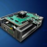
S2C Interfaces and Accessories

What are the considerations for choosing daughter cards or the FPGA prototyping systems that will hold the daughter cards? Well, the FPGA prototyping system you select should have abundant unused I/O pins on I/O connectors in order to use daughter cards. Naturally, the most important methods for evaluating a prototyping system in this regard is to examine the type of I/O connectors the system uses, how the pins are defined, the availability of different types of daughter cards and what features the FPGA board supports for using the daughter cards, so you do not have to build anything on your own.

S2C Request for Quote

The number of expansion connectors and types are important criteria when selecting suitable prototyping hardware. Of course, the more expansion connectors there are on the board, the more flexible it is. But keep in mind that the expansion connectors may also be used to interconnect between FPGA boards when design requires partitioning. The FMC connector is a good example that has many off-the-shelf daughter cards but because of its large footprint and pin definitions, it is not ideal to use as general interconnect between FPGA boards. As an example, S2C’s Prodigy Connector is a compact, high-performance, 300 pin connector that can support the running of multi-GHz transceivers. It supports 3 full FPGA I/O banks and all traces from the same I/O connector have the same length. The Prodigy Connector has a matching Prodigy Cable that can connect 2 Prodigy Connectors with pin 1 matching pin 1. The Prodigy Connector supplies 2 voltages from the FPGA board to the daughter board: 3.3V and VCCIO voltages.

A vast library of pre-tested daughter cards can save precious engineering time and reduce risks. Many of today’s chip interfaces use industry standards, such as USB, HDMI, PCIe, Ethernet, DDR, and others, and the commercial daughter card can meet the requirements. S2C has dozens of daughter cards coverring processors, embedded & multimedia, high-speed GT and memory applications. Take Prodigy 3 Channel RGMII/GMII PHY Interface Module as an example:

[LIST=1]

  • On the PCB or layout design stage, we have a rigorous design process to ensure the daughter card runs over 125MHz, so the Gigabit Ethernet can work well.
  • We implemented the auto-detection technology, so that the teams across the globe can identify the presence of specific daughter cards remotely and test on it.
  • The IO voltage detection function is integrated too, if somebody inputs a wrong voltage, the power will be automatically shut off to protect the hardware.
  • We also developed a reference design for it, within this, a customer can quickly bring up their designs.These daughter cards can be reused across multiple configurations of FPGA prototyping and among multiple projects/locations. The goal is to speed up and simplify customers’ system prototyping process.Another key consideration is whether the FPGA prototyping vendor can provide daughter card customization services. Off-the-shelf solutions solve many problems but sometimes special system interfaces or optimizations for specific SoC and ASIC applications are required. So customization services can be extremely beneficial especially when you are working on a time-to-market critical project. S2C has had numerous customization services over the past 15 years, the typical SOW covers schematic design, PCB layout, SI simulation (optional), manufacture, hardware initial bring-up and test design develop and delivery. Even if you would prefer to build the daughter card in-house S2C can provide the daughter card design guideline and support to speed your efforts and reduce risk of delays.

    About S2C
    Founded and headquartered in San Jose, California, S2C has been successfully delivering rapid SoC prototyping solutions since 2003. S2C provides:

    With over 200 customers and more than 800 systems installed, S2C’s focus is on SoC/ASIC development to reduce the SoC design cycle. Our highly qualified engineering team and customer-centric sales force understand our users’ SoC development needs. S2C systems have been deployed by leaders in consumer electronics, communications, computing, image processing, data storage, research, defense, education, automotive, medical, design services, and silicon IP. S2C is headquartered in San Jose, CA with offices and distributors around the globe including the UK, Israel, China, Taiwan, Korea, and Japan. For more information, visit www.s2cinc.com.


Forget the Saudis: Apple or Google should acquire Tesla

Forget the Saudis: Apple or Google should acquire Tesla
by Vivek Wadhwa on 09-02-2018 at 7:00 am

Steve Jobs wanted to build an electric car as far back as 2008. In 2014, Tim Cook reportedly funded the project. To date, though, Apple has had little to show for it, and the rumors are that its electric vehicle will launch as late as 2025— long after such things become common commodities. Google has already had self-driving electric cars on the road for about four years, though it has decided to focus primarily on the software.

A decade after Tesla announced the Model S, and six years after its delivery, no other company has been able to produce anything comparable. The big automotive manufacturers are claiming that they will soon eat Tesla’s lunch, but even the strongest offerings — those of BMW and Mercedes — are merely souped-up cassette players trying to compete with an iPod.

Tesla learned the hard way the intricacies of combining legacy automotive technologies with modern software — through trial and error and constant delay. It also struggled to automate production. Using advanced robots, however, it has finally figured out how to build an astonishing 6000 cars per week, some in a tent.

Now, as Tesla struggles with its cash balances, extremely negative press, and Elon Musk’s erratic tweets, it is at another crossroad and, in order to reach its potential, needs a strategic partner. It may not make sense for it to continue as a public company.

The best acquirer would not be Saudi Arabia, whose interest Musk tweeted about, because that nation’s interests inherently conflict with Tesla’s. Electric vehicles and solar technologies will cause the price of oil to plummet and decimate the value of Saudi oil reserves, so it would lose heavily if its investment in Tesla paid off. Technology companies, however, share Musk’s goals and ambitions, particularly Apple and Google. They have the money, technology, and marketing strengths to greatly enhance Tesla’s offerings. Apple also has great manufacturing prowess and distribution channels.

Tesla would provide Apple with an entirely new set of technology platforms on which it could build a new line of products. Apple desperately needs these in order to sustain its trillion-dollar market capitalization; after the release of the iPhone, in 2007, it has had virtually no world-changing products. It needs to enter new markets, and, with its automotive, energy storage, and solar technologies, Tesla would provide them.

Apple’s existing products would also benefit from the advanced technologies that electric cars have incorporated, such a batteries and in-car electronics. And Apple would gain the second-best self-driving software in the industry.

Tesla could, in turn, integrate the iPad, Apple TV, iTunes, and App Store into its automotives, literally turning its vehicles into iCars. And it could replace its clunky operating system with macOS. I am sure that all Tesla owners—such as me—would love to be able to download apps and music onto a console that’s more user friendly than the Tesla’s present one.

Apple would bring its world-class manufacturing and inventory-management process to Tesla and create new types of automobiles, in different sizes and shapes — and at lower prices. This would give it a second chance to wow markets it has largely lost; specifically India and China.

Google’s interests too coincide with Tesla’s. Google doesn’t have Apple’s manufacturing capability, but its maps and self-driving software are one or two notches above any other. Tesla’s mapping software is substandard, and its self-driving software can use a major upgrade. Google’s self-driving-car spinoff, Waymo, could focus on the software and let Google’s Tesla arm deal with the hardware.

Given that Morgan Stanley has just valued Waymo at $175 billion, Tesla’s $70 billion price would be a no-brainer, and the combination would be formidable.

Would Musk even entertain such an offer? Given that he reportedly turned down an offer from Google in 2013 and laughed off the idea of Apple’s buying Tesla in emails I exchanged with him in April 2014, and in an earningscall last year, it would seem very unlikely. Yet, having reached his personal limits and being close to burnout, as Musk has admitted; after seeing the disastrous impact of his tweet about having secured funding; and with Saudi Arabia offering investment in a competing startup, things may have changed.

I’ll bet that Musk would take an offer that solved his financial problems and gave him autonomy. With the headaches of funding and quarterly stock pressure taken away, the world’s greatest innovator would be free to develop world-changing ideas that transform entire industries, including automotive, energy, and space. That would be a win–win for Tesla — and for humanity.

For more, follow me on Twitter: @wadhwa and read my bookThe Driver in the Driverless Car


Apps Before there were Apps

Apps Before there were Apps
by Daniel Nenni on 08-31-2018 at 7:00 am

This is the thirteenth in the series of “20 Questions with Wally Rhines”

My development of a calculator program to determine the Black Scholes value for an option was not the only application that attracted financial people to programmable calculators. As the SR-52, and later TI 59, grew in popularity, and took market share from the HP 65, we began to discover a vast community of innovative people writing programs for these calculators. Peter Bonfield and Stavros Prodromou drove the formation of PPX -52 Professional Program Exchange, a forum where a contributor of a useful, well documented program could receive credits for the purchase of other programs. As these programs accumulated, TI moved to publish booklets of programs on various topics and sold them. Because of the success of my Black Scholes program, and because we were short of person power, I was appointed to provide management supervision for the PPX Xchange.

Each month, we met to review the new programs that had been submitted. It was at that point that I began to comprehend the enormous resource available to us. Thousands, maybe millions, of talented people wanted to demonstrate their expertise through programmable calculator programs. In most cases, they didn’t care if they were compensated. They just wanted to show other people how brilliant they were.

The ultimate example came when I reviewed a program for a “one armed bandit” that simulated a Las Vegas slot machine. By loading the program and then pressing “enter”, the display showed three single digit random numbers separated by dashes. Dashes? There were no dashes on the SR 52 or TI 59 calculators. How could they possibly have done this? It took one of our expert engineers to analyze the program and figure out how it worked. The creator of the program had discovered that execution loops could be created that would simultaneously display more than one number; since the segments in the LED displays were strobed at about 14 times per second, the program could create overlap and thus a dash between numbers. The program was so brilliant that we contacted the author to see if he wanted to work for TI. Similarly, the SR 52 had extra, undocumented registers that programmers discovered and used for applications that were not anticipated by the developers of the SR 52.

Over the next year, many communities of people became connected through their common interest in different applications. TI’s published booklets of applications carried contact information for the authors of programs. Although there was no internet for authors to communicate, they found ways to share information. TI then sponsored events to showcase the diverse set of applications available for the programmable calculators. I was asked to demonstrate my Black Scholes program at one of these events in New York City where analysts and others from the financial community were targeted. Ben Rosen, the Morgan Stanley semiconductor analyst who was the most respected in the industry, came to the event. He was fascinated with the Black Scholes program and invited me to tour the trading floor at Morgan Stanley. Later, he visited Lubbock, Texas (a major trip for a New York investment banker) and we showed him what we were doing. I continued to run into Ben at conferences and other events. And then, after I moved to Houston to run the Microprocessor Division, I received a strange phone call. It was Ben. He said that he was leaving Morgan Stanley and that he and L.J. Sevin were starting a venture capital fund. And he said that he would be in Houston the following week and wondered whether I would be able to have dinner with him and L.J. Of course, I was available.

Ben gave his pitch for how Sevin Rosen wanted to set up potential entrepreneurs and fund them while they worked on ideas for new businesses. That way, any conflict of interest with present employers could be avoided. I was flattered that they would think of me. In fact, I was amazed that they would make a trip to Houston just to talk with me. A few months later it became apparent that they had not come to Houston just to talk with me, as evidenced by the announcement that Sevin Rosen would fund Compaq Computer, a Houston startup headed by Rod Canion, another TI employee.

I didn’t take advantage of Ben and L.J.’s offer. My responsibilities were growing too rapidly at the time to consider leaving TI. But since Ben had to sell rights to his semiconductor newsletter, the Rosen Electronics Letter. Esther Dyson bought it and renamed it Release 1.0 and began the reorientation from semiconductors to software. She, along with George Gilder, continued some of the semiconductor theme. When TI announced the TMS 7000 8-bit microcontroller, I made a trip to New York and did a series of one hour interviews with representatives of various electronics journals. Gordie Campbell, then CEO of SEEQ, gave the presentation with me as our alternate source for the TMS 7000. Gordie highlighted the Ethernet controller that SEEQ had embedded in their version of the TMS 7000. After giving the presentation seven times during the day, Gordie and I became bored and we switched places; I gave his presentation and he gave mine. And that’s how we met Esther, who wrote up the announcement in her newsletter and then proceeded to invite us to speak at the PC Forum each year.

The 20 Questions with Wally Rhines Series


Analog IC design across PVT conditions, something new

Analog IC design across PVT conditions, something new
by Daniel Payne on 08-30-2018 at 12:00 pm

Transistor-level design for full-custom and analog circuits has long been a way for IC design companies to get the absolute best performance out of silicon and keep ahead of the competition. One challenge to circuit designers is meeting all of the specs across all Process, Voltage and Temperature (PVT) corners, so that silicon yields high enough to maximize profits. In the early days of my IC design career at Intel in the 1970’s we had a simple design methodology:
Continue reading “Analog IC design across PVT conditions, something new”


The Robots are Coming!

The Robots are Coming!
by Bernard Murphy on 08-30-2018 at 7:00 am

Moshe Sheier, VP Marketing at CEVA, recently got back from MWC Shanghai and commented that robots are clearly trending. He saw hordes of robots from dozens of companies, begging for someone to brand and offer them in any one of many possible applications: in an airport to guide you to a connecting flight, for elder care, in hospitals for food and drug delivery, in education for learning about robotics and programming but also as assistants in dealing with special needs kids, food delivery in restaurants, the list is endless. Think of this as the next big thing after smart speakers (Amazon already has 100k+ robots working in their warehouses, so obviously they’re working on home robots as a sequel to the Echo).


Which Moshe said made him think about what it will take to offer competitive robot solutions. He pointed me to Gartner’s list of the top 10 AI and sensing capabilities they believe will be needed in personal assistant robots by 2020, among which they (Gartner) include computer vision, a conversational user interface, biometric recognition / authentication, acoustic scenery analysis, location sensing, autonomous movement and of course local (edge) AI.

Why is it so important for all of this to be available in a robot? Why not let the cloud do the heavy lifting? There may be a scalability problem in that concept, but also we’re starting to get wise to why the cloud isn’t the answer to every need. Latency is an issue – if you want a quick response you can’t wait for a round-trip and possibly delay in getting a resource to do the work. Privacy/security is a big concern. Do you want you’re your medical symptoms or payment details exposed to eavesdropping hacks? Power is always a concern – robots aren’t much use when they’re parked at a power outlet. Having to go to the cloud and back burns significant power in communication. It often makes sense to do as much compute as possible locally, as counter-intuitive as that may seem.

Take computer vision – move it to the edge. But you have to be careful; dropping the cloud-based solution into a robot probably won’t work. You could handle vision on a leading GPU – positioning, tracking and gesture recognition are examples. Add more intelligence and the robot can find objects and people. But a big GPU used for graphics, intelligent vision and deep learning will be a real power hog. Not a problem in the cloud but a real issue on the edge. Offloading some of these tasks, particularly vision and a lot of recognition onto DSPs is a natural step since DSPs have a well-recognized performance per watt advantage over GPUs.

Autonomous movement requires ability to recognize and avoid objects which, unless the robot has to relearn object positions over and over again (slow and power hungry), requires an ability to build a 3D map of a room or floor of a building. Naturally this should be updated as objects move but that should only need incremental refinement. This again highlights the accelerating trend to move AI to the edge. Learning is typically thought of as a cloud-based activity, where trained networks are downloaded to the edge. But 3D-mapping and ongoing refinement can’t depend on cloud support (sorry I knocked the lamp over – I was waiting for a training update from the cloud?).

Acoustic scene analysis is a hot topic these days, extracting significant sounds or speakers from an acoustically busy background. The family is in the living room chatting away, the TV’s on and you want to ask your robot to answer a question. How does the robot figure out it’s being asked to do something and who asked? Or you’re away from the house and an burglar breaks a window or your dog starts barking. Can the robot understand there’s cause for concern?

This has to start with acoustic scene analysis – it doesn’t make sense to ship an unedited audio stream to the cloud and have that figure out what to do. A lot of intelligent processing can happen before you get into command recognition and even natural language processing (NLP). Separating sources, recognizing sounds like breaking glass and your dog barking, also keyword and some targeted command recognition, these can be processed locally today. General-purpose NLP will likely be a cloud (and continuing research) function for quite a while, but domain-specific NLP shows promise to be supported locally in the not too distant future.

So when you’re thinking about building that robot and you want to differentiate not just on features but also time to market and usability – a lot of the hard work already done for you and much longer uptimes between charges – you might want to check out CEVA’s offerings, in their platform for local AI, in front-end voice processing and in deep learning in the IoT.


ISO 26262: People, Process and Product

ISO 26262: People, Process and Product
by Bernard Murphy on 08-29-2018 at 12:00 pm

Kurt Shuler, VP Marketing at Arteris IP, is pretty passionate that people working in the automotive supply chain should understand not just a minimalist reading of ISO 26262 as it applies to them but rather the broader intent, particularly as it is likely to affect others higher in the supply chain. As an active ISO 26262 working group member, I guess he has better insight than many of us regarding latent problems that might emerge after an IP, chip or system has nominally been signed off. He makes the point that, in compliance, everyone through supply chain is still learning; a subtle problem at one stage might never become an issue or might eventually emerge only in integration testing in the car.


At each stage in the chain, it is the responsibility of the integrator to determine if vendors of the products they use can validate all the claims they make in asserting they and their product(s) are compliant with the standard. This isn’t just about the product. Kurt summarizes it as being about people, process and product. Claims are required in each of these areas. It can be temptingly easy to go with minimalist check-marks especially on people and process and still pass all requirements on handoff to the next stage. Then later you hear of a problem at a Tier-1 or an Uber or Waymo which might have been flagged as a potential concern in a more robust reading of compliance. Would this have been your fault? Probably not. Did you make money? Almost certainly not. Probably best to accept that participating in the design of a (successful) car these days needs to be a much more collaborative enterprise than it used to be. We all have responsibilities to bound as well as we can how our product may behave throughout the supply chain.

People training is an area where Kurt is clearly concerned about divergence between how he sees compliance being implemented versus the spirit of the standard, especially in IP development. The requirement calls for a trained functional safety manager supported (maybe) by (some) functional safety engineers. But the spirit of the standard calls for a sustainable safety culture which implies training, demonstrated competences and qualifications much more broadly across the organization. This can extend to executives, marketing personnel, engineering staff, documentation teams, quality assurance managers, application engineers and others. Proof of this training can be and often is required by customers and third parties who verify compliance. Obviously this requires a bigger investment but supply chain learning will likely tend over time to those who invest more in organization training.

Kurt also sees deficiencies in how people interpret Quality Processes. As engineers we naturally gravitate towards technologies and tools (requirements management, change management, verification, etc) to address this area but in his view, while these can play a role, this is the wrong place to start thinking about quality management.

Quality management systems (QMS) have been around for a while. You’ve probably heard of ISO 9001, there’s something called automotive SPICE (nothing to do with circuit simulation, this is for automotive software development) and Capability Maturity Model Integration (CMMI). These aren’t tools, they’re processes defining best practices for development and support, though some provide quite specific guidance for semiconductor and software IP development. What is important in demonstrating adherence to a quality process is choosing one of these QMS systems and demonstrating continual use of that system by all employees. Again, not something you can just delegate to the safety team.

In product, Kurt highlights a couple of points that maybe aren’t at the top of your safety checklist. You are designing an IP and someone else will be designing using that IP. Also your testing will not be based on testing the IP in the content of the car, or a Tier-1 system or even in the chip. These could be fairly significant limitations when it comes confidence in the safety of your component in that car. ISO 26262 gets around this by requiring the component provider to document assumptions of use that detail what is expected from the integrator in reasonable use of that component. But the integrator is likely also going to configure your IP and you don’t know what configuration they will ultimately use. Messy. So the standard requires IP vendors and chip integrators to agree upon a Development Interface Agreement (DIA) defining the assumptions used by and responsibilities of both parties. That takes a lot of thought and work on both sides.

Finally. Kurt has concerns about how well IP developers understand the intent behind and practice of failure mode analysis. The natural engineering bias is to get as quickly as possible to quantitative analysis to assess and grade mitigation mechanisms for potential failures – the FMEDA step. But he points out that first you have to spend quality time on the FMEA step, otherwise the FMEDA is meaningless. Unfortunately FMEA doesn’t have a lot of tool support that I’m aware of. This is just hard engineering judgment work, partitioning the design into manageable pieces, deciding what are possible failure modes in each piece, what are reasonable assumptions about the likelihood of those failures and what methods you are going to use to mitigate such failures (duplication, parity, …).

Altogether this is a lot of work and a bigger commitment than some vendors may have fully understood. But to survive the natural selection that will emerge in automotive supply chains, it may not be avoidable. You can get more detail by downloading Kurt’s technical paper.


An FPGA Industry Veteran’s View of Future

An FPGA Industry Veteran’s View of Future
by Tom Simon on 08-29-2018 at 7:00 am

There are tectonic changes happening in the world of FPGAs. A lot has changed since their introduction in the 80’s. Back then they were mostly used to implement state machines or glue logic. Subsequently they grew more complex with the addition of high speed IOs, eRAM, DSPs, other processors and other IP. More recently though FPGAs have come into the limelight because of their ability to help solve today’s data processing challenges. These include enhancing data center throughput and accelerating machine learning applications.

One person who has witnessed many of these changes is Manoj Roge, Achronix Vice President of Strategic Product Planning. During his career he has worked at both Xilinx and Intel (Altera) in strategic positions. I had the pleasure of talking with him about the changing landscape for FPGAs recently.

Microsoft showed with their Catapult project that FPGAs are extremely useful for accelerating datacenter workloads. This comes at a good time because CPU performance scaling is slowing due to the end of Moore’s law improvements previously provided by generational process improvements. Even multiprocessing using CPU architectures is not meeting the computational needs of today’s applications.

FPGA are inherently parallel and offer fewer constraints in many applications than GPUs. One of the big factors that helped GPUs grow in market share for general computing applications was the readily available development tools that allowed programmers to move applications to that platform. Similarly, Manoj pointed out during our conversation, FPGA programming is moving from RTL to coding languages like C++ and Python. This will have the effect of opening up the benefits of FPGA throughput to a much larger pool of application developers. Manoj was adamant that the quality and usability of development tools for FPGAs is crucial, especially now that the audience has expanded to include coders and not just hardware engineers.

According to Manoj, the other factor leading to the increased usage of FPGAs is the enormous mask costs for advanced nodes such as 16nm and beyond. It’s not unusual for a mask set to costs upwards of $10M. These higher costs are pushing system designers to build fewer, but more generally applicable, ASICs. Adding programmability to an ASIC through embedded FPGA is an ideal way to accomplish this.

Achronix is unique in having an embedded FPGA fabric. In concurrent with increasing masks costs, the cost per LUT has gone down, making the use of FPGA fabric for this purpose feasible. The dual advantage of embedded FPGAs are lower power and lower latency. Manoj pointed out that there are a number of papers that show a 10X reduction in power when the need to go off-chip is eliminated. The power overhead of driving IOs and maintaining signal integrity in board traces is huge. An on-chip embedded FPGA fabric avoids these power sinks. Latency also goes down with embedded FPGA fabric. Many applications call for microsecond scale latency, and an embedded FPGA fabric can deliver this.

Manoj told me that eFPGA is ideal for the new compute workloads found in AI/ML such as image classification and video recognition, real time video transcoding (4K/HD), 5G backhaul and baseband radio, and smart city and smart factory. While these systems may initially rely on off chip FPGA, as volumes ramp up on-chip FPGA becomes increasingly attractive.

FPGAs have a major role to play in the most advanced computing systems being used for the tide of emerging applications. Manoj sees that Achronix will be playing a major role in these markets. There is more information about Achronix eFPGA on their website.


Analytics and Visualization for Big Data Chip Analysis

Analytics and Visualization for Big Data Chip Analysis
by Tom Dillinger on 08-28-2018 at 12:00 pm

Designers require comprehensive logical, physical, and electrical models to interpret the results of full-chip power noise and electromigration analysis flows, and subsequently deduce the appropriate design updates to address any analysis issues. These models include: LEF, DEF, Liberty library models (including detailed CCS-based behavior), SPEF/DSPF, VCD/FSDB, etc. – the size of the complete chip dataset for analytics in current process nodes could easily exceed 3TB. Thus, the power distribution network (PDN) analysis for I*R voltage drop and current densities needs to be partitioned across computation cores.

Further, the simulation vector-based analysis (of multiple operating scenarios) to evaluate dynamic voltage drop (DvD) necessitates high throughput. As a result, elastically scalable computation across a large number of (multi-core) servers is required. Two years ago, ANSYS addressed the demand for computational resource associated with very large multiphysics simulation problems with the announcement of their SeaScape architecture (link).

Some Background on Big Data

Big data is used to:

  • Drive search engines, such as Google Search.
  • Drive recommendation engines, such as Amazon and Netflix (“you might like this movie”).
  • Drive real-time analytics, like Twitter’s “what’s trending”.
  • Significantly reduce storage costs — e.g. MapR’s NFS compliant “Big Data” storage system.

Big data systems require a key new concept. Keep all available data, as you never know what questions you’ll later ask. All big data systems share these common traits:

  • Data is broken into many small pieces called “shards”.
  • Shards are stored and distributed across many smaller cheap disks.
  • These cheap disks exist on cheap Linux machines. (Cheap == low memory, consumer-grade disks and CPU’s.)
  • Shards can be stored redundantly across multiple disks, to build resiliency. (Cheap disks and cheap computers have higher failure rates.)

Big Data software (like Hadoop) use simple, powerful techniques so the data and compute are massively parallel.

  • MapReduce is used to take any serial algorithm and make it massively parallel. (see Footnote [1])
  • In-memory caching of data is used to make iterative algorithms fast.
  • Machine learning packages run natively on these architectures. (see MLlib, http://spark.apache.org/mllib)

ANSYS SeaScape is modeled after the same big data architectures used in today’s internet operations, but purpose-built for EDA. It allows large amounts of data to be efficiently processed across thousands of cores and machines, delivering the ability to scale linearly in capacity and performance.

Simulation of advanced sub-16nm SoCs generates vast amounts of data. Engineers need to be able to ask interesting questions to perform meaningful analyses to help achieve superior yield, higher performance, lower cost – with the most optimum metallization and decap resources. The primary purpose of big data analytics is not simply to have access to huge databases of different kinds of data. It is to enable decisions based on that data relevant to the task at hand, and to do so in a short enough time that engineers can take action to adjust choices while the design is evolving. The SeaScape architecture enables this analytics capability (see the figure below).

RedHawk-SC

The market-leading ANSYS RedHawk toolset for power noise and EM analysis was adapted to utilize the SeaScape architecture – the RedHawk-SC product was announced last year.

I recently had the opportunity to chat with Scott Johnson, Principal Technical Product Manager for RedHawk-SC in the Semiconductor Business Unit of ANSYS, about the unique ways that customers are leveraging the capacity and throughput of RedHawk-SC, as well as recent features that provide powerful analytic methods to interpret the RedHawk-SC results to provide insights into subsequent design optimizations.

“How are customers applying the capabilities of RedHawk-SC and SeaScape?” I asked.

Scott replied, “Here are two examples. One customer took a very unique approach toward PDN optimization. Traditionally, P/G grids are designed conservatively(prior to physical design), to ensure sufficient DvD margins, with pessimistic assumptions about cell instance placement and switching activity. This customer adopted an aggressive ‘thin’ grid design, expecting violations to be reported after EM and DvD analysis – leveraging the throughput available, the customer incorporated iterations of RedHawk-SC into their P&R flow. A set of four ECO operations was defined, to address different classes of analysis issues. The ECO’s were applied in the P&R platform, and RedHawk-SC analysis was re-run. Blocks converged within two or three ECO + RedHawk-SC iterations – on average, the customer calculated they saved 7% in block area, as a result. And, this was all automatic, scripted into the P&R flow, no manual intervention required.”

“The second customer took a different, highly unique approach toward analytics of RedHawk-SC results. The SeaScape architecture inherently supports
(and ships with) a machine learning toolset. The customer had been utilizing senior designers to review EM results, and make a binary fix or waive decision on high EM fail rate segments. The customer implemented an EMWaiver ML application on the SeaScape platform – after training, EMWaiver is presented with the EM results, and its inference engine automatically evaluates the fix-waive decision.” Scott continued.


Illustration of the EM Assistant application, using the ML features of SeaScape

Scott highlighted that as part of the training process, the precision and accuracy of the ML-based flow was assessed. The precision relates to the inferred “fix” designation that could have been waived, requiring additional physical design engineering resource – a precision factor of ~90% was reported (implying ~10% extra fixes). The accuracy relates to the risk of an inferred “waive” that actually requires a fix – the customer was achieving 100% accuracy, as required (i.e., no “escapes”).

“Sounds pretty advanced”
, I interjected. “How would new customers leverage the model information and analytics detail available, after executing RedHawk-SC?”

Scott replied, “We have added a MapReduce Wizard interface in RedHawk-SC. Users progress through a series of menus, to select the specific design attributes of interest – e.g., cell type, cell instances, die area region – followed by the electrical characteristics of interest – e.g., cell loading, cell toggle rate, perhaps specific to cell in the clock trees.”

The figures below illustrate the steps through the RedHawk-SC MapReduce Wizard, starting with the selection of the design model view, and then the specific electrical analysis results of interest.

RedHawk-SC MapReduce Wizard menus for analytics – model data selection


MapReduce Wizard electrical analytics selection — e.g., power, current, voltage

“The MapReduce functional code is automatically generated, and applied to the distributed database.” , Scott continued. “An additional visualization feature in RedHawk-SC creates a heatmap of the analytics data, which is then communicated back to the user client desktop. Design optimizations can then quickly be identified – if a different analytics view is required, no problem. A new view can be derived on a full-chip model within a couple of minutes. Multiple visual heatmaps can be readily compared, offering an efficient multi-variable analysis of general complexity.”

An example of a heatmap graphic derived from the analytics data is depicted below – this design view in this example selected clock tree cells.

Scott added, “In addition to these user-driven analytics, there is a library provided with a wealth of existing scenarios. And, the generated MapReduce code is available in clear text, for users to review and adapt.”

I mentioned to Scott, “At the recent DAC conference there was a lot of buzz about executing EDA tools in the cloud. The underlying SeaScape architecture enables a very high number of workers to be applied to the task. Is RedHawk-SC cloud-ready?”

Scott replied, “SeaScape was developed with the explicit support to run on the cloud. It’s more than cloud-ready – we have customers in production use on a(well-known)public cloud.”

“The level of physical and electrical model detail required for analysis of 5nm and 3nm process node designs will result in chip databases exceeding 10TB, perhaps approaching 20TB. Design and IT teams will need to quickly adapt to distributed compute resources and elastic job management like SeaScape, whether part of an internal or public cloud.”
, Scott forecasted.

The computational resources needed to analyze full-chip designs have led to the evolution of multi-threaded and distributed algorithms and data models. The ability to efficiently identify the design fixes to address analysis issues has traditionally been a difficult task – working through reports of analysis flow results is simply no longer feasible. Analytics applied to a chip model consisting of a full set of logical, physical, and electrical data is needed. (Consider the relatively simple case of a library cell design that correlates highly to DvD or EM issues – how to quickly identify the cell as appropriate for a “don’t_use” designation required big data analytic information).

The combination of the SeaScape architecture with the features of ANSYS analysis and simulation products addresses this need. For more information on RedHawk-SC, please follow this link.

-chipguy

PS. Thanks to Annapoorna Krishnaswamy of ANSYS for the background material on Big Data applications and the ANSYS SeaScape architecture.

Footnote

[1] Briefly, MapReduce refers to the functional programming model that has been widely deployed as part of the processing of queries on very large databases – both Google and the Hadoop developers have published extensively on the MapReduce programming model. The “Map” step involves passing a user function to operate on (a list of) data shards, the same function executing on all workers. The result of executing the Map step is another list, where each entry is assigned a specific “key”, with an associated data structure filled with values. A simple example would be a text file parser function, where the keys are the “tokens” generated by the parser, and the data value is a count of the number of instances of that token (calling a “compress” or “combine” function after individual token parsing).

The next step is to “shuffle” the (key, value) records from the Map step, to assign the records to the specific “Reduce” node allocated to work on the key. All the records from each Map node for the key are sent to the designated Reduce node. As with the Map(function) step, a Reduce(function) step is then executed – Reduce is often referred to as the “aggregation” step. Again using a text parser as the example, the Reduce function could be a sum of the count values received from all the Map nodes for the key, providing the total instance count for each individual token throughout the input text file.


Overview of MapReduce


Illustration of the MapReduce architecture used by Hadoop

The data analytics features in SeaScape are based on the MapReduce programming model. An excellent introduction to MapReduce is available here.


WEBINAR: A UVM Cookbook Update

WEBINAR: A UVM Cookbook Update
by Bernard Murphy on 08-28-2018 at 7:00 am

Something I always admire about Mentor is their willingness to invest their time and money in helping the industry at large. They do this especially in verification where they sponsor periodic Wilson surveys on the state of verification needs and usage in the industry. More recently they introduced their UVM Cookbook, an introduction to help new users and also I’m sure a handy reference to the more arcane corners of the standard for experienced UVM practitioners. Of course a challenge in any how-to guide to an evolving standard is that it inevitably drifts out of date. So Mentor recently released an update, aligned with the IEEE 1800.2 release, which should encourage freshers to seniors to turn to this guide to learn, as a reference and to dip into as a great source of examples.


Check out the Mentor Webinar on September 11[SUP]th[/SUP] at 8am Pacific.

To help me out, Tom Fitzpatrick (Strategic Verification Architect at Mentor) and I first talked about where UVM adoption is these days. While older methodologies (“e”, VMM etc) still claim their adherents, based on the latest Wilson survey UVM is fast becoming the methodology of choice, especially in ASIC design but also starting to see traction in FPGA design. No doubt this is because of the huge learning and legacy investment in testbenches. You don’t want to have to rework that – for any reason. UVM is widely supported and current so is becoming the standard of choice for verification methodology going forward.

That said, when an old-timer like me looks at the Cookbook (on-line, no-one uses paper books anymore) it can seem pretty overwhelming. Where do you start, and do you have to understand the whole thing before you can become effective? All that complexity is needed to handle the significantly higher complexity of verifying the systems we build today, but Tom told me not to panic. Most verification engineers don’t need to digest the whole thing. A few UVM experts will likely build the majority of the infrastructure most teams will need, leaving lesser mortals like me to assemble tests based on a much less demanding understanding of the standard. Following the cookbook metaphor, you can be a superchef and cook a 7-course gourmet meal from scratch if you choose, or you can go the BlueApron route, have most of the work already done for you (by your internal experts) and be able to throw together a great one-pot meal with minimal effort. Encouraging to hear that there’s a reasonably gentle learning curve for us beginners. Starting with, naturally a newly-added Basics section in the Cookbook.

What’s new in this version? Tom tells me of course it is fully updated to 1800.2 and especially all the examples are fully updated. They also archived all the OVM material that had been included in the earlier version – useful back then but largely unnecessary for today’s UVM users.

The main point he stressed for this update is a single recommended architecture to support emulation-friendly UVM testbenches. As emulation plays an increasingly important role in system verification, it becomes essential to ensure that testbenches can migrate with minimal change to emulator-based flows. To accomplish this, the Cookbook recommends split transactors communicating with the DUT through transaction methods rather pin-level driver/monitor components. If you are familiar with this approach, you’ll know one side of the transactor sits with the DUT (on the emulator) and the other side sits in the testbench. Transaction-level rather than signal-level data exchange allows the emulator run at faster speeds than would be possible if required to sync with the testbench on signal-level changes.

The Cookbook recommended methodology is closely aligned with the (open) UVM Framework and Questa VIP so you can spin-up quickly with a methodology that ensures your testbench development will be emulator-friendly. Tom mentioned a number of other improvements to the Cookbook, including (among others) updates to the Register Abstraction Layer reflecting changes in 1800.2, an updated UVM Connect chapter for those of you wanting to drive verification from higher-level TLM abstractions and a chapter consolidating information on messaging in UVM.

I won’t and can’t steal their thunder because there’s way too much to cover in a blog. Tom recommends that for those of you who are interested, you should register for their Webinar on September 11[SUP]th[/SUP] at 8am Pacific where I know you’ll get a much more expert summary of this update.


GLOBALFOUNDRIES Pivoting away from Bleeding Edge Technologies

GLOBALFOUNDRIES Pivoting away from Bleeding Edge Technologies
by Daniel Nenni on 08-27-2018 at 3:00 pm

It’s no secret that I have been a big fan of GLOBALFOUNDRIES since they came about in March of 2009. We even included them in our first book “Fabless: The Transformation of the Semiconductor Industry” right next to TSMC. I am also a big fan of pivoting which is the term we use here in Silicon Valley to describe some of the most innovative technology turnarounds. Apple going mobile is one of my favorite pivots, Nvidia is also a pivot master, Intel not so much. As a foundry connoisseur I knew most of the challenges GF would face but the challenges were much greater than even I expected, absolutely.

TSMC has always been a fierce competitor but the Apple partnership makes them unbeatable in my opinion. The new “node per year” cadence that Apple requires to launch new products every September has turned out to be a devastating pivot for the other foundries. Not only does it keep Apple ahead with bleeding edge silicon, it helps TSMC introduce new process technology ecosystems at a dizzying pace.

So yes, GF will skip 7nm and below and join the ranks of UMC, SMIC, TowerJazz etc… as a boutique foundry which can be quite profitable. In fact, with CMOS, FinFET, and the FD-SOI offerings, I would crown GF the King of the Foundry Boutiques!

So where does that leave us on the bleeding edge? TSMC and Samsung. My prediction is that the new Intel CEO will do some refocusing and Intel Custom Foundry will not be part of it.

Upside
Remember that GF 7nm capacity is 15k WPM versus the massive 7nm capacity of TSMC and Samsung so there will be no shortages based on this announcement. Also, AMD and TSMC agreed on this months ago to secure 7nm capacity so this is pure upside for TSMC and possibly Samsung. Will AMD and others use Samsung for a second source? My guess is yes because that is how the foundry business has always worked. AMD already second sources Samsung 14nm. At 7nm AMD will stay with TSMC but at the lower nodes they will straddle TSMC and Samsung, my opinion.

Downside
The semiconductor equipment companies may take a small hit even though GF can re-purpose the 7nm line for 14/12nm but that still leaves ASML EUV machines orphaned. It is also not clear what the IBM Power PC people will do for leading edge silicon moving forward.

There is much more to discuss here so let’s do it in the comments section. And don’t forget, GLOBALFOUDNRIES, Samsung and TSMC all have events coming up in September and October. This announcement will make them that much more interesting.

Here is AMD’s response:

Expanding our High-Performance Leadership with Focused 7nm Development

AMD’s next major milestone is the introduction of our upcoming 7nm product portfolio, including the initial products with our second generation “Zen2” CPU core and our new “Navi” GPU architecture. We have already taped out multiple 7nm products at TSMC, including our first 7nm GPU planned to launch later this year and our first 7nm server CPU that we plan to launch in 2019. Our work with TSMC on their 7nm node has gone very well and we have seen excellent results from early silicon. To streamline our development and align our investments closely with each of our foundry partner’s investments, today we are announcing we intend to focus the breadth of our 7nm product portfolio on TSMC’s industry-leading 7nm process. We also continue to have a broad partnership with GLOBALFOUNDRIES spanning multiple process nodes and technologies. We will leverage the additional investments GLOBALFOUNDRIES’ is making in their robust 14nm and 12nm technologies at their New York fab to support the ongoing ramp of our AMD Ryzen, AMD Radeon, and AMD EPYC processors. We do not expect any changes to our product roadmaps as a result of these changes…

And the official PR from GF:

GLOBALFOUNDRIES Reshapes Technology Portfolio to Intensify Focus on Growing Demand for Differentiated Offerings

Semiconductor manufacturer realigns leading-edge roadmap to meet client need and establishes wholly-owned subsidiary to design custom ASICs

Santa Clara, Calif., August 27, 2018 – GLOBALFOUNDRIES today announced an important step in its transformation, continuing the trajectory launched with the appointment of Tom Caulfield as CEO earlier this year. In line with the strategic direction Caulfield has articulated, GF is reshaping its technology portfolio to intensify its focus on delivering truly differentiated offerings for clients in high-growth markets.

GF is realigning its leading-edge FinFET roadmap to serve the next wave of clients that will adopt the technology in the coming years. The company will shift development resources to make its 14/12nm FinFET platform more relevant to these clients, delivering a range of innovative IP and features including RF, embedded memory, low power and more. To support this transition, GF is putting its 7nm FinFET program on hold indefinitely and restructuring its research and development teams to support its enhanced portfolio initiatives. This will require a workforce reduction, however a significant number of top technologists will be redeployed on 14/12nm FinFET derivatives and other differentiated offerings.

“Demand for semiconductors has never been higher, and clients are asking us to play an ever-increasing role in enabling tomorrow’s technology innovations,” Caulfield said. “The vast majority of today’s fabless customers are looking to get more value out of each technology generation to leverage the substantial investments required to design into each technology node. Essentially, these nodes are transitioning to design platforms serving multiple waves of applications, giving each node greater longevity. This industry dynamic has resulted in fewer fabless clients designing into the outer limits of Moore’s Law. We are shifting our resources and focus by doubling down on our investments in differentiated technologies across our entire portfolio that are most relevant to our clients in growing market segments.”

In addition, to better leverage GF’s strong heritage and significant investments in ASIC design and IP, the company is establishing its ASIC business as a wholly-owned subsidiary, independent from the foundry business. A relevant ASIC business requires continued access to leading-edge technology. This independent ASIC entity will provide clients with access to alternative foundry options at 7nm and beyond, while allowing the ASIC business to engage with a broader set of clients, especially the growing number of systems companies that need ASIC capabilities and more manufacturing scale than GF can provide alone.

GF is intensifying investment in areas where it has clear differentiation and adds true value for clients, with an emphasis on delivering feature-rich offerings across its portfolio. This includes continued focus on its FDX[SUP]TM[/SUP] platform, leading RF offerings (including RF SOI and high-performance SiGe), analog/mixed signal, and other technologies designed for a growing number of applications that require low power, real-time connectivity, and on-board intelligence. GF is uniquely positioned to serve this burgeoning market for “connected intelligence,” with strong demand in new areas such as autonomous driving, IoT and the global transition to 5G.

“Lifting the burden of investing at the leading edge will allow GF to make more targeted investments in technologies that really matter to the majority of chip designers in fast-growing markets such as RF, IoT, 5G, industrial and automotive,” said Samuel Wang, research vice president at Gartner. “While the leading edge gets most of the headlines, fewer customers can afford the transition to 7nm and finer geometries. 14nm and above technologies will continue to be the important demand driver for the foundry business for many years to come. There is significant room for innovation on these nodes to fuel the next wave of technology.”

About GF
GLOBALFOUNDRIES is a leading full-service semiconductor foundry providing a unique combination of design, development, and fabrication services to some of the world’s most inspired technology companies. With a global manufacturing footprint spanning three continents, GLOBALFOUNDRIES makes possible the technologies and systems that transform industries and give clients the power to shape their markets. GLOBALFOUNDRIES is owned by Mubadala Investment Company. For more information, visit http://www.globalfoundries.com.

Contact:
Jason Gorss
GLOBALFOUNDRIES
(518) 698-7765
jason.gorss@globalfoundries.com