I don’t know if it was just me but I left TechCon 2017 feeling, well, uninspired. Not that they didn’t put on a good show with lots of announcements, but it felt workman-like. From anyone else it would have been a great show, but this is TechCon. I expect to leave with my mind blown in some manner and it wasn’t. I wondered if the SoftBank acquisition had knocked them a little off their game.
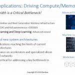
This year they seem to have got their mojo back, at least judging by a press announcement I joined before the show. ARM is again swinging for the fences, this time in announcing a major initiative for cloud to edge infrastructure support and a new processor roadmap to support that direction. Of course ARM is already well-known in the edge but they’re also deeply embedded in base-stations, top of rack switches, gateways and WAN routers. In fact ARM claims the largest market share in units for processor IP in infrastructure (I’m sure intended as a reminder that RISC-V is still a toddler in markets already dominates).
They’re also starting to have some impact in the server space (the cloud in its various manifestations), though another person on the call asked if that initiative is struggling given e.g. Qualcomm’s exit. Drew Henry, the speaker and VP/GM for the Infrastructure BU, acknowledged the QCOM change but said there will be announcements at TechCon on new server entrants which apparently will demonstrate ample continuing momentum.
So what’s the big deal with infrastructure? ARM anticipates significant growth in this area given their expectation of a trillion devices in the IoT. Smart parking and city lighting, retail, transportation and many other applications will create many wireless edge nodes needing to communicate ultimately with the cloud. And that will require layers of intelligent data reduction and traffic management between those levels; mega-servers and 5G alone won’t be enough to manage the data volume.
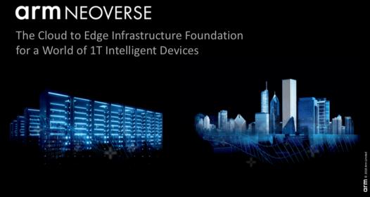
So ARM has announced NEOVERSE, which diverges from the Cortex world. NEOVERSE is a brand we were told and is inclusive of technologies and services that partners will bring to the space. ARM’s contribution under this brand starts with high-performance secure IP and architectures. Drew showed us a roadmap for these IP, starting with the Cosmosplatform, related to the A72, A75 and available today in 16nm. The next step up will be the Aresplatform, available in 2019 at 7nm. Following Ares in 2020 we’ll get the Zeusplatform in 7nm+ and in 2021 we’ll see the Poseidon platform at 5nm. Drew expects about 30% improvement per generation in performance and features.
The next component of NEOVERSE is a wide range of solutions and, of course, an extensive ecosystem. The solutions don’t look too dissimilar from what you know around standard ARM offerings, though with perhaps with more networking options and multiple accelerators, from ML and embedded FPGA to video. In the ecosystem they already have endorsements from multiple silicon and EDA providers, most of the US and Chinese cloud providers (I didn’t notice Google), big systems names like Ericsson, Nokia, Huawei and Cisco and Sprint, Orange and Vodaphone among others in operators.
In OS they include RedHat, Suse and Oracle, in container/virtualization they have Docker, OpenStack, VMWare, etc. In language and library support they have endorsements from OpenJDK, Python, NodeJS and GO, in devtools they listed codefresh, shippable and more. Finally in Open source projects for networking and server they include Linaro (naturally), LF networking and Cloud Native Computing Foundation. Apparently some of this work is already underway, eg Ares is starting to appear in Linux builds. Overall not a bad starting point.
The third component of NEOVERSE is scalability. Naturally the level of solutions you want to see in the cloud will be different from what you would expect in connectivity, or the fog, or near the edge. In the cloud you want TBps and lots of cache, handling datacenter workloads. In networking, storage and security you still need performance but not at the same scale and you need the hardware features required to support workloads like NFV, SDN, IPSec and compression. At the edge, or close, demands are not nearly as challenging, though still possibly requiring support for virtualization and certainly support for wireless and/or wired upload.
This feels like more than just another arrow in ARM’s quiver. It’s an additional quiver with arrows crafted to a very distinct target, again with strong ecosystem support. Which should help them further expand the gap between ARM and alternative solutions. At least I’m sure that’s how ARM sees it.