RVN! 26 Banner revised (800 x 100 px) (600 x 100 px)

Wi-Fi Standards Simplified

Wi-Fi Standards Simplified
by Bernard Murphy on 11-01-2018 at 7:00 am

In the world of communications, the industry fairly quickly got a handle on a naming convention for cellular technology generations that us non-communication geeks could understand – 2G, 3G, 4G and now 5G, (though some of us could never quite understand the difference between 4G and LTE, at least as those terms are widely and no doubt inexpertly used). This is a nice steady progression, easy for us uncultured masses to remember, with no confusing affixes.

Bluetooth has from the beginning followed a largely similar convention in generation naming from 1.0 up to current BT 5 which drops the ”.0” on the name, not coincidentally aligning numerically with the latest cellular standard. There is a sub-generation of 4.0 (at least initially), known widely as BLE (Bluetooth Low Energy) but we generally understand that this is a low-energy variant on the underlying standard.

Wi-Fi on the other hand soldiered on in geekdom, oblivious to the needs of the masses, by sticking a bewildering array of postfixes on the root 802.11 standard name. I guarantee that no-one in the general public would have any idea what you were talking about if you asked them about say 802.11n, whereas many would profess at least some familiarity with 5G, if with the name only. The Wi-Fi Alliance recognized this wasn’t great for marketing and has recently switched to a much easier naming convention, at least for the most recent generations.

For the newer generations of the standard, 802.11n becomes Wi-Fi 4, 802.11ac becomes Wi-Fi 5 and 802.11ax becomes Wi-Fi 6. For 802.11a/b/g I hear differing stories. Fortune magazine says that these names won’t change. Another contact says (plausibly) that these will be known as Wi-Fi generations 1, 2 and 3. Now isn’t that easier to understand? You may not know what they are but all of us can understand that as you progress from Wi-Fi 1 to Wi-Fi 6, you get better technology at each stage, for which you are prepared to shell out more money (see, that’s marketing).

We’re a bit more sophisticated than that, so what are 4-6? Wi-Fi 4 (aka the “n” version) supports transmission rates 5-6 times faster than the Wi-Fi 3 version, higher reliability and supports MIMO (multi-input, multi-output) where multiple antennae at receiver and/or transmitter further boost reliability and transmission rates.

Wi-Fi 5 (aka the “ac” version), introduced in 2014, increases rates by a factor 2 or more and more efficiently uses bandwidth so more users can be served at speed in one network. However, more efficient usage is only in the downlink. So you can all watch cat videos with minimal buffering but the network bogs down if you all want to share with friends. Wi-Fi 6 (aka the “ax” version), expected to be ratified by the end of 2019, goes one step further, packing multiple users more effectively in both downlink and uplink, serving an expected 4X improvement in throughput in high user density environments (think of a stadium). It also offers a 25% improvement in peak data rate.

So Wi-Fi generation naming is now understandable and mostly aligned with cellular and Bluetooth naming. There’s an apparent disconnect in that the latest Wi-Fi is Wi-Fi 6, whereas cellular is at 5G and Bluetooth is at BT5. But the official Wi-Fi 6 is a year away so perhaps numeric synchronization isn’t too far off. When we’re checking out phones or other devices, we should reasonably soon be able to look for all communications to be at level “N” (maybe 6?) no matter what the underlying technology. That will make life a lot simpler, certainly for me.

I have to thank Franz Dugand, Sales and Mktg Director for Connectivity at CEVA for these insights. Naturally CEVA has a wide range of Wi-Fi IPs across these standards, including Wi-Fi 6, ranging from low-power to high-performance to multi-gig rates. CEVA have been in the Wi-Fi core licensing business since 2002 so they’re very well known and established in the space. You can learn more about their RivieraWaves Wi-Fi platforms HERE.


Architecture for Machine Learning Applications at the Edge

Architecture for Machine Learning Applications at the Edge
by Tom Dillinger on 10-31-2018 at 2:01 pm

Machine learning applications in data centers (or “the cloud”) have pervasively changed our environment. Advances in speech recognition and natural language understanding have enabled personal assistants to augment our daily lifestyle. Image classification and object recognition techniques enrich our social media experience, and offer significant enhancements in medical diagnosis and treatment. These applications are typically based upon a deep neural network (DNN) architecture. DNN technology has been evolving since the origins of artificial intelligence as a field of computer science research, but has only taken off recently due to the improved computational throughput, optimized silicon hardware, and available software development kits (and significant financial investment, as well).

Although datacenter-based ML applications will no doubt continue to grow, an increasing focus is being applied to ML architectures optimized for “edge” devices. There are stringent requirements for ML at the edge – e.g., real-time throughput, power efficiency, and cost are critical constraints.

I recently spoke with Geoff Tate, CEO at Flex Logix Technologies, for his insights on ML opportunities at the edge, and specifically, a new product emphasis that FlexLogix is undertaking. First, a quick background on DNN’s.

Background

A “deep” neural network consists of multiple “layers” of nodes. At each node, a vector set of inputs is provided to a computational engine. The output of each node is further refined by a (potentially non-linear) activation function calculation, which is then forwarded to the nodes in the next layer. The final layer provides the DNN decision from the original input set – i.e., a “classification” result of an input image to a reference set of objects.

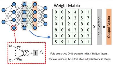
Figure 1. Illustration of a simple DNN, with 3 “hidden layers”. The computation at each layer is a matrix multiplication of the input vector and a matrix of weights.

Numerous DNN topologies are used in practice – the figure above depicts a simple, fully-connected multi-layer 2D design. (More complex “3D” topologies and implementations with feedback connections in the hidden layers are often used, which are optimal for specific types of inputs.)

Each node in the DNN above performs several computations, as shown in the figure below. At each node in the layer, a set of weights are multiplied against the input value, then summed – i.e., a “multiply-accumulate” (MAC) calculation. An (optional) bias value may be incorporated into the sum at each node. The MAC output is input to a normalizing “activation” function, which may also incorporate specific parameter values – activation function examples are illustrated below.

Figure 2. Expanded detail of the calculation at each node in a layer, and some examples of activation functions.

During the DNN training phase, a reference set of inputs is applied. The selection of the initial weights, biases, and activation parameters at each node is an active area of research, to optimize the training time. (The simplest method would be to pick values at random from a normalized distribution.) The input reference set proceeds throughforward evaluation and the DNN result compared to the expected output.

An error difference is calculated at the output layer. A backwards optimization phase is then performed, evaluating an error gradient dependence for the network parameters. Internal DNN values are then adjusted, and another forward evaluation pass performed. This training optimization iterates until the DNN classification results demonstrate acceptable accuracy on the input reference set.

The DNN values from training are subsequently used as part of the production inference engine, to which user data is now the input.

DNN in the Data Center

The initial DNN (training and inference) implementations in the datacenter utilized traditional von Neumann CPU and (DRAM) memory resources to perform the MAC and activation calculations. The DRAM bandwidth to the CPU core is typically the throughput bottleneck.

A transition to GPU-based cores for DNN calculation was then pursued, to leverage the SIMD dot product MAC calculations prevalent in GPU image processing. GPU’s have a drastically different architecture, with very wide internal vector datapaths – e.g., ~1024 bits wide. As a result, to improve core resource efficiency, a “batch” of inputs is evaluated concurrently – e.g., 32b floating-point DNN parameter values could be concatenated into a wide vector to evaluate a batch size of 32 inputs in parallel through the DNN layers. Yet, the local memory associated with each GPU core is relatively small (KB’s). Again, the (GDDR) memory bandwidth is a DNN performance-limiting factor.

New chip architectures are being aggressively pursued for ML applications – e.g., Google’s Tensor Processing Unit (TPU). And, due to the intense interest in the growing base of ML applications, numerous chip start-ups have recently received (initial round) VC funding – see the figure below.

Figure 3. Examples of ML hardware startups (from [1]).

Additionally, cloud service providers are deploying FPGA hardware to offer effective, easily-reconfigurable DNN capabilities. [2]

DNN’s using conventional CPU and GPU hardware architectures are throttled by the access bandwidth to retrieve the weights and biases for each layer evaluation. Training presents an additional data constraint as these parameter values are required to compute both the forward evaluation and the backward optimization error gradients, as well. As an example, the ResNet-50 DNN is commonly used as a reference benchmark for image classification, a complex (3D) 50-layer convolutional network topology. A forward pass evaluation utilizes ~26M weights. [3] Depending upon the data precision of these parameters, the memory bandwidth required to access these values for use in a layer computation is very high.

ML Applications at the Edge

My conversation with Geoff at Flex Logix was very enlightening. First, he shared some of the characteristics of edge applications.

“An ML application will typically pursue DNN training at the datacenter, and then transfer the DNN parameters to edge hardware for inference.”

“Often, a DNN hardware implementation quotes a peak throughput, in trillions of operations per second (TOPS), and a related power efficiency (TOPS/W). Yet, it is important to analyze what memory bandwidth and batch evaluation assumptions are used to calculate that throughput.”

“Edge customers will typically be utilizing (sensor) input data corresponding to ‘batch_size = 1’. Maybe a batch size of 2 or 4 is applicable, say if there are multiple cameras providing video frames per second input. The datacenter architectures that merge parallel input sets into large batch size DNN evaluations to optimize MAC efficiency just don’t apply at the inference edge.”

“High batch count increases overall classification latency, as well, as the parallel input set is being merged – that’s of little consequence for typical datacenter applications, but additional latency is not appropriate at the edge.”

I asked Geoff, “How is Flex Logix approaching this opportunity at the edge? What elements of the existing embedded FPGA technology are applicable?”

Geoff replied, “We have announced a new product initiative, NMAX. This architecture builds upon many of the existing features of our embedded FPGA, specifically:

  • a tile-based building block that is readily arrayed into an (m X n) configuration
  • a combination of logic LUT cell and MAC engines in a DSP-centric tile
  • a method for optimal embedding of SRAM macros of varying size between tiles (link)
  • a rich set of external connectivity options when embedded within an SoC design

A block diagram of a single “NMAX512” tile is illustrated below.

Figure 4. An architectural block diagram of the NMAX512 DNN tile, and an array of tiles depicting the L2-level SRAM between tiles.

Each tile contains 8 NMAX clusters. Each cluster contains 64 MAC’s using an 8b x 8b parameter data width (with options for 16b x 16b), with a 32b accumulate. There is a total of 512 MAC’s per tile. The programmable EFLX logic LUT’s perform the activation functions for the DNN layer. The weight and bias values for the layer are accessed from the local (L1) SRAM within the tile.

An embedded (L2) SRAM between tiles stores the intermediate DNN results and parameter values for successive layer calculations. New values are loaded into the L2 SRAM in the background during forward evaluation. The required data bandwidth for system DRAM memory is reduced significantly.

Geoff added, “The time to reconfigure the NMAX tile with new DNN layer with new DLL layer data (from L2) is very fast, on the order of 100’s of nsec.”

“How is the NMAX tile implementation for a DNN developed?”, I inquired.

Geoff answered,“ML developers utilize the familiar TensorFlow or Caffe languages to define their DNN topology. We will be releasing a new NMAX implementation flow. Users provide their TF or Caffe model, and the NMAX compiler fully maps the data and logic operations to the MAC clusters and reconfigurable EFLX LUT logic. All the sequencing of DNN layer evaluation is mapped automatically. The physical LUT placement and logic switch routing configuration is also automatic, as with a conventional embedded FPGA.”

Geoff continued, “Our preliminary performance models indicate we will be able to achieve ~1GHz clocking (TSMC 16FFC), or roughly ~1 TOPS throughput per tile(with LPDDR4 DRAM, L2 SRAM size optimized for the DNN). The distributed L2 SRAM helps maintain a very high MAC and activation function utilization.”

“Speaking of performance modeling, do you have NMAX benchmark data?”, I wondered.

Geoff replied, “We prepared the following data for NMAX compared to other architectures, such as the Nvidia Tesla T4, for the ResNet-50 DNN benchmark with Int8 parameters. Note that the NMAX architecture enables a wide span of tiled array sizes, with corresponding throughput scaling for the batch_size = (1, 2, 4) of greatest interest to edge customers. The initial MAC utilization and total power dissipation is much improved over other architectures, as well.”

Finally, I asked, “What is the NMAX deployment schedule?”

Geoff answered, “We are starting to engage partners now, in terms of potential NMAX sizes of interest. Our engineering team will be finalizing IP area/performance/power specs in 1H2019, as well as finalizing the NMAX compiler. A tapeout release with a specific tile and SRAM configuration will occur in 2H2019, to provide evaluation boards to customers.”

There is clearly a lot of activity (and VC investment) pursuing optimized DNN hardware architectures for datacenter applications. There is certainly also a large market for (embedded IP or discrete) hardware focused on the power/perf/cost constraints of the low batch-size ML applications at the edge. Flex Logix is leveraging their expertise in reconfigurable (DSP plus logic) functionality in pursuit of this opportunity.

It will be an interesting R&D area to follow, for sure.

-chipguy

References

[1]https://origin-blog.appliedmaterials.com/vc-opportunities-ai-developer-ecosystem

[2]Putnam, A., “The Configurable Cloud — Accelerating Hyperscale Datacenter Services with FPGA’s”,2017 IEEE 33rd International Conference on Data Engineering (ICDE),https://ieeexplore.ieee.org/document/7930129/ .

[3]https://www.graphcore.ai/posts/why-is-so-much-memory-needed-for-deep-neural-networks


Mentor’s Busy ITC and Major Test Product Updates

Mentor’s Busy ITC and Major Test Product Updates
by Tom Simon on 10-31-2018 at 1:00 pm

In conjunction with the 2018 International Test Conference, Mentor has several interesting test announcements. They also have a busy round of technical activities, including a number of technical papers, presentations, tutorials and a poster from a major customer about using Mentor. I’d like to touch on the two product related announcements, because they are pretty interesting.

There is probably no area other than automotive where reliability has received more focus lately. First off, zero defects are a prerequisite for ISO 26262. Also, the automotive semiconductor market is experiencing higher growth rates than almost any other sector. As such, automotive applications have become the reference for quality and reliability. It is pushing the development of improved methodologies and is setting the standard for the highest reliability.

Automotive is on a steep complexity growth curve, both historically and for the immediate future. It used to be that automotive semiconductors could leisurely stay behind the bleeding edge of technology. However, ADAS and new requirements for infotainment have brought automotive computing and data transfer requirements to the point where only the most advanced nodes will suffice. Going from Level 2 to Level 4/5 for ADAS will increase the number of sensor modules by around a factor of 5. Higher levels of automation will require more complex computational tasks. For example, AI algorithms may be used to anticipate pedestrian movements to help avoid auto versus pedestrian conflicts. All of this adds up to more complex chips and more of them, which will necessitate increased effort to ensure the highest reliability.

To address the needs of this market Mentor has added a new set of test patterns to deal with failure modes found in FinFET processes and 3D transistor structures. Mentor Tessent TestKompress already looks at each cell to determine areas that are vulnerable to defects. Now they are adding analysis that will look at cell to cell interactions looking for potential defect sources. Several Tessent customer are publicly reporting significant reductions in their DPPMs, in the ranger of 700 to 4300, by using the improved analyses offered in Mentor’s automotive-grade ATPG.

With the added automotive-grade test patterns it should be possible to replace many system level or functional test patterns. Mentor has added automated pattern generation that targets critical-area based interconnect bridges and opens, as well as cell internal and neighborhood defects.

Mentor’s other announcement concerns improving the efficiency of silicon bring-up. Mentor has created a networked connection between the DFT software and the testers themselves. They worked with Teradyne to interface UltraFLEX ATE to Tessent SiliconInsight. Because literally hundreds of IP blocks are being added into new SOC designs, IJTAG has seen strong adoption. With this comes the need for IJTAG debug tools. With the introduction of Mentor’s Interactive IJTAG, designers can get better insight into what is happening on the tester, right in their test software in real-time. Reduced iteration time can shorten bring-up from weeks to days. Interactive IJTAG speeds up the many complex mappings that are needed to generate the test program on the tester and then interpret the test results in a way that is meaningful to the designer.

The 2018 ITC features papers from Tessent customers discussing real world results with TestKompress Automotive-grade ATPG and SiliconInsight Interactive IJTAG. Mentor is vigorously involved in improving the state of the art in test. This shows in their ISO 26262 qualification for use on all ASIL ISO 26262 projects. System designers and end customers are the beneficiaries of their sustained efforts in test. There are more details on these new announcements and Mentor Test products on their website under TestKompress or SiliconInsight.


Parasitic Extraction for Advanced Node and 3D-IC Designs

Parasitic Extraction for Advanced Node and 3D-IC Designs
by Alex Tan on 10-31-2018 at 7:00 am

Technology scaling has made positive impacts on device performance, while creating challenges on the interconnects and the fidelity of its manufactured shapes. The process dimension scaling has significantly increased metal and via resistance for advanced nodes 7nm and onward, as shown in figures 1a,1b. Similar to a fancy smartphone without a good wireless carrier quality (4G/LTE or 5G), a higher performance device is deemed an unattractive option as it needs to be accompanied by optimal wirings in order to minimize net delay attributed latency. Hence, to accurately measure design targets, capturing interconnect contribution during IC design implementation is crucial.

Challenges to parasitic extraction
From a designer’s standpoint, a good parasitic extraction solution should address accuracy, performance, capacity and integration aspects.

Accurate modeling of wire capacitances in an advanced node process is a non-trivial task as it is a function of its shape, context, distance from the substrate and to surrounding wires. It eventually leads to solving the electrostatic field in a region involving multiple dielectrics. The more heterogeneous design trend employing innovative and complex packaging has also necessitated the augmentation of existing extraction techniques with 3D-IC modeling capability (see figure 1c).
As design size is growing, both the extraction file size and turn-around time increases –to reflect the jump in design net count, extracted RC networks size and its associated physical representation or layers handling. Capacity works both ways: the extraction tool of choice should be capable of absorbing a large design, do the extraction and produces an extraction file that is reasonably compact to be back-annotated in downstream timing analysis stage. All of these should be done fast, too.

Apart from managing route resources or interconnect (by means of pre-routes, layer assignments and route blockages), having an accurate and robust parasitic extraction technology is also essential in helping to pinpoint hot-spots due to ineffective utilization of wires or vias, and any potential signal integrity related issues. The extraction step should be interoperable with either the analysis or the optimization tools that will consume the parasitics data points.

Modeling, extraction accuracy and xACT
Both device and interconnect modelings hold critical role in providing accurate parasitic values. With device architecture transitioning to non-planar, multi-gate architecture such as FinFET and the upcoming the Gate All Around (GAA) structures, the current density and parasitic capacitance between the gate and source/drain terminals is expected to increase with further technology scaling.

During the micrometer process technology era, field-solver techniques for capacitance extraction was reserved for correlation purposes as it provided good results accuracy but was computationally expensive. We were also accustomed to labeling 2D, 2.5D, or pseudo-3D modes to RC extraction. Recently, there are many field-solvers and its variations noted (from finite element to boundary element based and to the most recent floating random-walk method). While accuracy is traditionally achieved through discretization of the parasitic equation by means of table lookup, such approach is inadequate with the increased layer and design complexity.

Calibre xACT™ is Mentor’s high-performance parasitic extraction solution. It combines fast, deterministic 3D field solver and accurate modeling of physical/electrical effects of complex structures/packaging used in advanced nodes –to deliver needed extraction accuracy, including rotationally invariant total and coupling capacitances.

In order to address RC extraction of heterogeneous design such as a 3D-IC with FOWLP (Fan-Out Wafer-Level Packaging), xACT applies a 3D-IC modeling by taking into account two interface layers between the neighboring dies as shown in figure 2. It captures their interaction and creating an ‘in-context extraction’ which offers highly accurate and efficient extraction results –with 0.9% error and 0.8% for the total ground capacitance and total coupling capacitances, respectively.

xACT also handles new interconnect modeling requirements at all layers such as accounting potential shift in BEOL due to multi-patterning impact on coupling capacitance, MOL contact bias modeling, Line-End Modeling (LOM), etc.

Extraction size reduction techniques
SPEF/DSPF and log files are notoriously ranked top on IT’s disk-space screener list. These files though normally retained in a compressed format, are still huge and can strain not only disk space, but also downstream simulators’ capacity –so reducing the parasitic size while not losing the overall accuracy is key.

Unlike some parasitic extraction methods’ reliance on the use of threshold or tolerance value as basis for parasitic size reduction, xACT is resorting to a more efficient reduction mechanism known as TICER (TIme Constant Equilibration Reduction). Electrically-aware TICER produces a smaller RC network while controlling the error. This feature can be used across design flows (analog, full-custom and digital sign-off).

A trial on a 128K SRAM design shows 30% faster timing simulation a parasitic netlist with TICER reduction (figure 3) when compared to an unreduced netlist, while the simulation error was within 2% compared to the unreduced netlist (figure 4).

Multi-corner interconnect extraction is usually a requirement for cell characterization and design sign-off as they have to be performed across multiple process corners. The introduction of multi-patterning at advanced nodes adds even more corners. For example, due to multi-patterning at 7 nm, the original nine process corners gets expanded to more than a dozen, since each has one or more multi-patterning (MP) corners. Instead of running each process corner separately –which is costly, xACT performs simultaneous multi-corner extraction, in which all process, multi-patterning, and temperature corners are extracted in a single run. The user specifies the desired combination of corners to extract and netlist, which is done after a LVS run.

Speed, capacity and integration
Because designs are also growing in complexity at each successive node, a big challenge for parasitic extraction at 7nm is processing the design and the necessary corners without incurring additional cycle time during the signoff phase. xACT solution handles all of these complex modeling requirements and utilizes a net-based parallelism with multi-CPU processing to deliver fast and accurate RLC parasitic extraction netlists. It enables full-chip extraction of multi-million instance nanometer design with multi-threaded and distributed processing architecture.

Advanced technology scaling has also introduced increased geometrical variabilities induced by the uncertainties in the manufacturing processes. Such variations of the manufactured devices and interconnect structures may cause significant shift from their design intent –the electrical impact of such variability on both the adjoining devices and interconnects should be assessed and accounted for during signoff.

Performance is multidimensional. From implementation perspective, design performance is not a function of the characterized library and wire choices only, but might be influenced by signal integrity induced delay. On the other hand, reliability analysis such as EM and self-heating are becoming more common and augmented as part of sign-off, xACT provides device location information to these tools to ensure current density violations can be accurately identified and resolved. Subsequent corrective actions such as via doubling and wire spreading can be taken to reduce current density occurrence.

The Calibre xACT platform also uses foundry-qualified rule decks in the Calibre SVRF language, and is interoperable with the Calibre nmLVS™ tool and with industry-leading design implementation platforms.

For more details on Mentor’s Calibre xACT, please check HERE.


Solving and Simulating in the New Virtuoso RF Solution

Solving and Simulating in the New Virtuoso RF Solution
by Tom Simon on 10-30-2018 at 12:00 pm

Cadence has done a good job of keeping up with the needs of analog RF designs. Of course, the term RF used to be reserved for a thin slice of designs that were used specifically in RF applications. Now, it covers things like SerDes for networking chips that have to operate in the gigahertz range. Add that to the trend of combining RF and digital blocks onto one die or into the same package and the scope of analog RF designs expands pretty rapidly.

Nevertheless, there were a few noticeable holes in the Cadence solution when it came to addressing RF designs. In the case of simulation, different parts of the design often resided in Allegro SiP or Virtuoso, so integrating and managing pre and post layout simulation was problematic. The other hole for RF users were the options available for EM solver based model generation and simulation. However, Cadence has expended a lot of effort to resolve these issues in their new Virtuoso RF Solution, and the results look pretty promising.

I had a conversation with Michael Thompson, RF Solutions Architect at Cadence, about the work they have recently done to improve the entire solution. His first point was that it used to be OK to do design separately, but changes in IC and package design mean that many more things are being combined and need to be looked at in a unified way. Thus, Virtuoso and Allegro SiP should to work together for RF designs. This created a requirement for lowering the barriers to exchanging design data between the systems, creating free bidirectional data exchange. They added the ability to concurrently use multiple technologies for simulation and layout. The key is to have one golden schematic for the entire design, including the package and multiple die, inside of Virtuoso.

The other hole they needed to plug was integration with EM solvers to make the flow seamless. Previously Cadence relied on a patchwork of external solvers integrated with SKILL code through the Connections Program. Of course, Cadence had their FEM solver that came in through the Sigrity acquisition. However, it was really targeted at board and package level problems as evidenced by its SiP integration. The majority of IC solvers are Method of Moments. Cadence struck a partnership with National Instruments to integrate their AWR Axiem tightly into Virtuoso. At the same time, they also created a path for Sigrity in the IC flow.

With seamless integration for extraction and simulation set-up, the ease of adding RF models for critical structures has improved dramatically. The models are S-parameter, but Spectre-RF has also improved its S-parameter handling. As a circuit’s design progresses, designers can move from QRC, to FEM and MoM, while keeping each of these as separate extracted views. The Hierarchy Editor allows swapping models for the simulation runs.

For the Virtuoso RF solution, Cadence has also been working on new device models. One example that Michael brought up was GaAs models.

Their solution brings together package and IC design into one environment where difficult RF design problems can be solved more easily. This new solution was shown for the first time at IMS. Ensuring that teams working on the package and on the IC can share data and analysis results makes sense with the growing complexity of RF designs. For more information on the new Cadence Virtuoso RF Solution, I suggest looking at the solution page on their website.


A Smart Way for Chips to Deal with PVT Issues

A Smart Way for Chips to Deal with PVT Issues
by Tom Simon on 10-30-2018 at 7:00 am

We have all become so used to ‘smart’ things that perhaps in a way we have forgotten what it was like before many of the things we use day to day had sensors and microprocessors to help them respond to their environment. Cars are an excellent example. It used to be commonplace to run down your battery by leaving your lights on. Now cars are smart enough to turn them off if left on too long. Even better illustrations are how cars adapt to driving at elevation or warm up smoothly when cold. There were simple mechanical gizmos that tried to compensate for operating conditions, but they were prone to malfunction or operating poorly. The use of monitoring has completely changed how reliable things are and how well they can adapt to changing conditions.

What we sometime fail to appreciate is that SOCs need to be smart in the same way. If my car can adjust the fuel mixture to compensate for temperature or oxygen levels, then why shouldn’t ICs adjust automatically for things like metal variation, operating voltage or even local temperature levels? If ICs can be made smart then performance, reliability and even yield will improve. Moortec is an IP provider that has been focusing on in-chip monitoring for almost a decade. They have sensors and controllers that can be embedded in SOCs during design that can help measure, adjust and compensate for a large variety of issues that occur in ICs during operation and over time as they age.

The most basic use of PVT sensors is to expedite and facilitate testing. Chips can be rapidly binned and proper operation can be verified by checking internal performance characteristics. However, there is a lot to gain by moving beyond using in-chip sensors for test and using them to dynamically manage chip operation.

Chips endue stress from higher self-heating with newer process nodes and the higher densities that they bring. Electrical overstress, electro migration, hot carrier aging, and increased negative bias temperature instability all threaten IC operation. Likewise, IR drops caused by increased gate capacitance, more resistive metal, and even supply issues can cause performance degradation or even failure. Additionally, process variation is harder to control because of new variation sources, multiple thresholds and the effects of ageing.

Moortec has been working on this problem since 2010, with their focus on in-chip monitoring systems. They have put together a system that uses several different sensor IP blocks that can be placed one or more times on the die. They tie these sensors together with a PVT controller which can be used to support DVFS/AVS, clock speed optimization, silicon characterization, and increased reliability and device lifetime.


Their process monitoring IP block uses multiple ring oscillators to assess device and interconnect properties. With the results of this sensor it is possible to perform speed binning, age monitoring and report timing analysis.

The voltage monitoring IP block is extremely versatile. It can monitor IR drop, core and IO voltage domains, and facilitates AVS. At the same time, it also helps monitor the quality of the supplies. It is useful in detecting supply events, perturbations, and supply spikes. An interesting feature is the ability to use one instance to monitor multiple supply domain channels in FinFET nodes.

The last leg of the triad is their temperature sensor. It has high accuracy and resolution and offers a number of testability features together with variable sampling modes to allow higher sampling rates if needed for performance.

High reliability and performance both require in-chip monitoring. In each of the critical markets for semiconductors today, it is necessary to squeeze out every ounce of performance while ensuring reliable operation. In safety critical systems such as ADAS, monitoring proper functioning and detecting age related failures is mandatory. Mobile devices need to operate at the lowest power possible, so DVFS is almost always used. In servers, high operating speed generate significant heating which even when minimized can still affect chip operation.

Moortec’s solution looks like it offers IP that is easily deployable to make chips smarter. I just wish that my parents’ carbureted Pontiac I drove in high school had the smart features that today’s technology provides. However, talking about that is a little bit like complaining about what a hassle dial phones were back in the day. That said, it seems inevitable that all chips will be smart soon enough. More information about
Moortec’s in-chip monitoring IP is available on their website.


The Latest from Samsung Semiconductor

The Latest from Samsung Semiconductor
by Tom Dillinger on 10-29-2018 at 12:00 pm

Earlier this Spring, Samsung Foundry held a technology forum, describing their process roadmap and supporting ecosystem developments (link). Recently, the larger Samsung Semiconductor organization conducted a Tech Day at their campus in San Jose, presenting (and demo-ing) a broader set of products. The focus of the day was on Samsung memory technology, encompassing non-volatile flash, DRAM, and GDDR roadmaps. The audience was more focused on system design and integration than silicon process technology, and the key Tech Day announcements reflected new Samsung memory products being introduced. (Samsung Foundry also made a major announcement.) Here are the highlights from the Samsung Tech Day.

Interesting Facts, Figures, and Quotes
In addition to the product introductions, there were some “sound bites” from the presentations that I thought were quite interesting:

  • “EUV lithography for DRAM manufacture is currently in R&D, not yet in production – it will no doubt be introduced in future DRAM generations.” (a few layers)
  • “Every 2 years, we create more data than we previously created in all of history.” (e.g., 160 ZB in 2025)
  • “Facebook generates 4 PB/day alone.”
  • “A future Class-5 fully-autonomous vehicle will generate 4TB/day.”
  • “Analytics are changing the way in which professional sports are being played. The defensive strategies being employed against individual hitters have resulted in the lowest overall Major League Baseball batting average in 46 years.”
  • “5G communications will be rolled out to 19 metropolitan areas in 2019.” (including San Francisco)
  • “Data center corporations are aggressively adding a Corporate AI Officer (CAIO)executive position.”
  • “Memory holds the key to AI.”

The focus of these examples was the requisite data capacity and bandwidth required of the current set of workloads. The key conclusion was:

“In the past few decades, computing evolved to a client-centric model. We are now moving to a memory-centric compute environment.”

One cautionary comment was provided:

“A significant percentage of the (unstructured) data being generated for analytics is ROT – redundant, obsolete, or trivial. A requirement for these memory-centric, data-driven applications will be to optimize the working dataset.”

Here are the major product announcements from the Samsung Tech Day.

256GB RDIMM

Samsung introduced the 16Gb DDR4 DRAM in 2017, utilizing their “1y nm” process technology. At the Tech Day, a 256GB “3D stacked” Registered DIMM stick was introduced. Although there’s been lots of attention given to 2.5D and 3D topologies for multiple (heterogeneous) logic die in a package, Samsung has been in production with stacked memory die for several generations – see the figure below.

Compared to an equivalent configuration with 2 x 128GB RDIMM, the 256GB RDIMM provides a ~25% power reduction, obviously a key factor in server design.

As the new RDIMM offers 2X the memory capacity in the same footprint, the maximum memory footprint of compute servers is likewise increased – e.g., 8TB in a 32-DIMM, 2P rack-mounted server. “In-memory” database transaction processing capabilities are expanded. For chip design, I was specifically thinking about the EDA applications for SoC electrical analysis, which are now able to accommodate 2X the model complexity, as well.

7LPP in Production
Although the theme of the Tech Day was the synergy between the Samsung Semiconductor product family and “memory-centric computing”, there was a major Samsung Foundry announcement, as well.

The “full EUV” 7LPP foundry process is now in full production, with comprehensive “SAFE” ecosystem support from EDA and IP partners.

Bob Stear, Senior Director, Samsung Foundry Marketing, indicated, “7LPP offers a 40% area reduction, and a 20% performance or 50% power improvement compared to 10nm. We are achieving a sustained exposure power output of 250W, enabling a throughput exceeding 1500 wafers per day. The utilization of single-exposure EUV lithography is truly a big leap in cost-effective production, compared to previous multipatterning-dominated process nodes. The number of masks is reduced by 20%.”

The figure above depicts the improved fidelity associated with (single-mask) EUV exposure versus (multi-patterned) 193nm ArF-immersion lithography.

Bob also hinted at future Samsung Foundry offerings, namely:


  • (2nd generation) 18FD-SOI, w/embedded Magneto-resistive MRAM
  • follow-on nodes 5LPE and 4LPE (E = “early” adopter), with PDK’s available in early 2019
  • (more info to come at the next Samsung Foundry Forum in May’19)
  • 3GAA (Gate-All Around) in 2019

“Smart” Solid-state Drive Architecture
A very unique announcement was the “Smart SSD”, a design that integrates an FPGA into the SSD package.

Xilinx collaborated with Samsung on the product engineering, offering a full application development and software library stack for the (Zynq, with ARM-Cortex core) FPGA integrated into the SSD.

The CEO of Xilinx participated in the product announcement, saying, “This new computational SSD architecture moves acceleration engines closer to the data, offering improved performance for database tasks and machine learning inference.”

Examples were provided of ~3X performance of (parallel-query) DB TPC-H transaction processing and ~3X business intelligence analytics (MOPS) throughput.

The Smart SSD architecture does present some interesting acceleration opportunities, and also some challenges. The endurance specifications for SSD’s vary significantly.

The system integrator utilizes the anticipated data communications workload profile to match the SSD endurance with the product requirements – e.g., an SSD “boot device” with limited activity (~0.1 – 1.0 effective drive writes per day, DWPD) to hard drive data caching (3++ DWPD). The use of an SSD in a new set of applications, such as providing accelerator engine data, requires new workload profiling and considerations for endurance reliability analysis (and over-provisioning) – a very interesting area for further research, to be sure. (The figure below provides an example of the SSD endurance calculations for Samsung SSD’s – a very interesting whitepaper is available here.)

Samsung Semiconductor definitely presented a unique perspective at their Tech Day, highlighting the need to focus on storage capacity and bandwidth for a new “memory-centric” computing environment.

-chipguy


Intel Q3 2018 Jibber Jabber

Intel Q3 2018 Jibber Jabber
by Daniel Nenni on 10-29-2018 at 7:00 am

This is what happens when you have a CFO acting as a semiconductor CEO, and Robert Holmes is a career CFO with zero semiconductor experience or education. Granted, no way did he write the opening statement, but it was full of jibber jabber anyway. The real disappointing jibber jabber was from our own Murthy Renduchintala on the status of 10nm which has been a trending topic on SemiWiki and elsewhere for many months. Why Intel thought they could jibber jabber their way out of 10nm questions I do not know. It started with Bob’s opening statement which in no way did he write:

While our current product lineup is compelling, our roadmap is even more exciting. We continue to make good progress on 10-nanometer. Yields are improving, and we’re on track for 10-nanometer-based systems on shelves during the holiday 2019 selling season. The breadth of IP we’ve assembled combined with Intel’s design, software, packaging, and manufacturing capability, gives us an unmatched ability to invent the industry’s future.

Bob, your current product lineup is compelling for one single reason, you have no real competition at 14nm. Intel 14nm is by far superior to TSMC 16nm and Samsung/GF 14nm in both performance and density. Unfortunately, that lead ends now with TSMC and Samsung 7nm which makes your current product lineup an offense to Moore’s Law and the industry leading Intel Tick-Tock model that we all knew and loved.

And the Murthy 10nm Jibber Jabber in the Q&A:

Venkata S. M. Renduchintala – Intel Corp.
Hey, Vivek, let me take it. This is Murthy. First of all, as Bob said in his opening remarks, the progress we’ve made in the quarter is very much in line with our expectations. While we can’t give any specific numbers, I do believe that the yields as we speak now are tracking roughly in line with what we experienced in 14-nanometer.

So we’re still very much reinforcing and reaffirming our previous guidance that we believe that we’ll have 10-nanometer shipping by holiday of 2019. And if anything, I feel more confident about that at this call than I did on the call a quarter ago. So we’re making good progress and I think we’re making the quarter-on-quarter progress that’s consistent with prior generations having reset the progress curve.

“While we can’t give any specific numbers”? Sure you CAN but you just won’t. Are they that embarrassing? How about a little transparency? And you wonder why the fake news about 10nm getting cancelled got traction? Murthy, since you were not at Intel during the 14nm yield ramp let me remind you that it was disastrous. So where exactly are 10nm yields in relation to 14nm?

Now that TSMC is in HVM with 7nm, which is comparable in performance and density to the much delayed Intel 10nm, not only CAN you disclose specific yield or defect density numbers, investors should be demanding it! It was embarrassing how the analysts on the call did not push for more information.

The full Intel Q3 2018 transcript is here.

The good news is that Intel had a fantastic quarter but AMD not so much. Hopefully this will change when AMD has 7nm parts out early next year but I would not bet on it. Even after losing the process lead the Intel sales organization is getting VERY aggressive and protective of their lead customers. I have seen examples of this first hand and I am seriously impressed. Intel is not walking away from price competitive deals, absolutely.

Intel +3.6% on beats, Data Center recovery, and positive guidance
Q3 results that beat EPS and revenue estimates driven by a recovery in Data Center, which missed estimates last quarter. Upside Q4 guidance has revenue at $19B (consensus: $18.39B) and EPS of $1.22 (consensus: $1.09). Revenue breakdown:

Client Computing, $10.2B (+16% Y/Y; consensus: $9.33B)
Data Center, $6.1B (+26%; consensus: $5.89B); IoT, $919M (+8%; consensus: $952.4M)
Non-Volatile Working Memory Solutions, $1.1B (+21%; consensus: $1.14B)
Programmable Solutions, $496M (+6%; consensus: $526.8M)

AMD Q3 revenue miss, weak guidance
Q3 results missed revenue by $50M with a reported $1.65B. Non-GAAP EPS narrowly beat by a penny at $0.13 but GAAP EPS missed by as much with $0.09.Computing and Graphics missed consensus with $938M in revenue (+12% Y/Y/ -14% Q/Q) compared to the $1.05B estimate. On the year growth was driven by Ryzen desktop and mobile products sales, partly offset by lower graphics sales.

The other notable news is that Intel publicly addressed fake news from a well known rumor site claiming that Intel 10nm had been cancelled. It has been discussed on SemiWiki in detail amongst actual working semiconductor professionals who found it to be fake news. The rumor site of course still stands by the report and that pretty much sums up the state of American media today. Thumbs up to Intel on this one. Let’s hope a legal response is being considered.

SemiAccuratehas learned that Intel just pulled the plug on their struggling 10nm process. Before you jump to conclusions, we think this is both the right thing to do and a good thing for the company.

Intel News
✔@intelnews
Media reports published today that Intel is ending work on the 10nm process are untrue. We are making good progress on 10nm. Yields are improving consistent with the timeline we shared during our last earnings report.
8:42 AM – Oct 22, 2018


Update October 22, 2018@3:30pm: Intel has denied ending 10nm on Twitter. The full tweet is, “Media reports published today that Intel is ending work on the 10nm process are untrue. We are making good progress on 10nm. Yields are improving consistent with the timeline we shared during our last earnings report.” SemiAccurate stands by its reporting.

Also read:
Intel Slips 10nm for the Third time?
Intel delays mass production of 10nm CPUs to 2019
Intel 10nm process problems — my thoughts on this subject
Kaizad Mistry on Intel’s 10 nm Technology (PDF)


Is Your BMW Secure?

Is Your BMW Secure?
by Roger C. Lanctot on 10-28-2018 at 7:00 am

The cybersecurity of automobiles has become an increasingly critical issue in the context of autonomous vehicle development. While creators of autonomous vehicles may have rigorous safety and testing practices, these efforts may be for naught if the system are compromised by ethical or unethical hackers.

Establishing cybersecurity in a motor vehicle is a daunting proposition. Cars are exposed in unprotected areas such as parking garages and public roadways much of the time they are in operation. Cars are also increasingly connected to wireless cellular networks and nearly all cars built after 1996 are equipped with an OBD-II diagnostic port enabling physical access to vehicle systems.

The proliferation of smartphone connection solutions such as Android Auto, Apple Carplay, the CCC Consortium’s MirrorLink and the SmartDeviceLink Consortium’s SDLink have also opened a path to cybersecurity vulnerability. All of these attack surfaces were used by Tencent’s Keen Security Labs when the organization identified 14 vulnerabilities in BMW vehicles earlier this year.

It is hardly shocking the Keen found these vulnerabilities. What is shocking was BMW’s response.

As a member of the Auto-ISAC, based in the U.S., BMW was obliged to report vulnerabilities to the membership – encompassing upwards of 50 car companies and their suppliers – within 72 hours. Instead, BMW waited more than three months. (Note: It is possible that the part of BMW that was notified of the hack by Keen was not in touch with the BMW executives representing the company within the Auto-ISAC.)

]During that time, between notification by Keen and notification of the Auto-ISAC, BMW worked directly with Keen engineers and scientists to remedy the flaws found by Keen. In fact, there are multiple videos available online that describe the details of the hacks and the efforts to correct them – which included over-the-air software updates, a capability that reflected BMW’s design foresight.

BMW concluded the episode by giving Keen the first ever BMW Group Digitalization and IT Research Award and pledging to collaborate closely with Keen in the future. BMW was Keen’s second “victim.”

Two years ago Keen remotely hacked a Tesla Model S also resulting in fixes from Tesla delivered via over-the-air software updates. Keen performed a second Tesla hack a year later and ultimately Keen parent Tencent took a 5% stake in Tesla.

It’s not clear whether Tesla was a member of the Auto-ISAC at the time of the Keen hacks or whether it reported those hacks in a timely manner. But there are lessons to be learned from both hacks.

1. Even the most sophisticated cars designed by some of the cleverest engineers in the industry have been found to be vulnerable to physical and remote hacks;

2. In a world where cars are increasingly driven based on the guidance of software code, cybersecurity is suddenly an essential concern for which there is no immediate, obvious fix;

3. Over-the-air software update technology is a key part of the solution;

4. Car companies must report cybersecurity attacks and vulnerabilities in a timely manner – mainly because so many components and so much code is shared across multiple car makers;

5. Car makers are obliged to constantly test their own systems and foster bug bounty programs and ethical hacking of their own systems to identify vulnerabilities in a proactive manner.

Unlike cybersecurity hygiene for mobile devices, consumer electronics or desktop computers, car makers cannot wait until they are hacked to respond. Car makers must be in a constant state of cybersecurity vigilance and testing.

This need is reflected in a recent announcement from Karamba Security. The company has launched its ThreatHive. ThreatHive implements a worldwide set of hosted automotive ECUs in simulation of a “car-like” environment for automotive software system integrators.

According to Karamba: “These ECU software images are automatically monitored to expose automobile attack patterns, tools, and vulnerabilities in the ECU’s operating system, configuration and code.” In other words, Karamba is embedding pen testing of systems into the development cycle of automotive systems.

The Karamba solution reflects the fact that car makers cannot wait for an intrusion and the lengthy product development life cycle requires a means of hardening automotive systems prior to market launch. As for automotive cybersecurity generally or the security of a given BMW particularly, cars may never be fully or certifiably cybersecure.

Car makers need to come clean with their industry brethren via organizations such as the Auto-ISAC and, ultimately, must be honest with their customers. If BMW knows my BMW is insecure, they better let me know and let me know how they are going to or how they have fixed that vulnerability.

In the video describing the remediation a BMW engineer says that the corrective measures are “transparent” to the vehicle owner who “will not notice the difference.” Unfortunately, BMW appears to have misunderstood the meaning of “transparent.” When correcting cybersecurity flaws, car makers must disclose, not hide, their work to protect the consumer. That may be the biggest lesson of all from the Keen Security Lab hack of BMW and may be one of the more difficult obligations for the industry to accept.


Semiconductor stocks free fall as bad news gets worse

Semiconductor stocks free fall as bad news gets worse
by Robert Maire on 10-26-2018 at 12:00 pm

Semiconductor stocks have had another significant down leg as the bad news continues to pile on. Bad news in this case doesn’t come in threes , it comes in droves. TI is perhaps very scary news as it is a rather broad based supplier of semiconductors that has fared better than more pure play chip suppliers. TI gave weak guidance that was broad based which echoes TSMC last weak giving less than stellar predictions.

The “chip flu” which started with the memory sector has now spread tp a full blown, cyclical down turn, epidemic. Analysts continue to capitulate even though many stocks are off by close to 50%. The horse bolted months ago through the open barn doors. We have very few analysts left to capitulate as there exist “perma-bulls” who never go negative despite the news.

We are quickly closing in on a “it can’t get much worse” scenario. The only things worse would be a trade war that would be the “coup de grace” for the industry.

We would remind investors that “bad” is a relative term. In the early cyclical days of the semiconductor industry, almost every company lost money in a cyclical downturn. Now most everyone is making money, just less of it, yet the stocks behave like we are on are way to red ink.

We are only part way through earnings season so that negative flow of news is not yet over. We can’t imagine much positive news that will come out of companies yet to report.

The good thing about all this bad news is that sooner or later we will be so bad that things can only get better, we may not be far from that point.

We still don’t know the shape of the down cycle, whether its a “U” or canoe or “L” shaped bottom, its obviously not “V” shaped.

AMAT is almost at the $30 price point we suggested. Lam is not that far from our $130 view. KLAC has broken through $90. We had said for a long while that AMD was way overdone and it was off by 9% today as it plummets back to earth.

With current sentiment, even good news and good guidance will not elicit a positive reaction in the stocks.

At this point the end of the quarterly reporting season can’t come soon enough to slow the decline.

Is Samsung a canary in a tech coal mine?
Earlier in 2018, Samsung essentially halted capex spending for its display business. This was followed shortly by their memory capex “push out” (maybe now turned into a cancellation).

Our reaction to these data points was much more negative than others as we view Samsung as one of the smarter CAPEX spenders in tech and their slow down had very ominous overtones which are now playing out.
Samsung should likely know better that any tech company, even Apple, what demand is looking like. They have the broadest based, consumer facing, tech exposure of any company in the world. They sell everything from TVs and dishwashers to smart phones and key components to frenemies like Apple.

If anyone would see a tech downturn coming it would be Samsung
They seemed to be voting with their feet as they were the first to cut spending on CAPEX when things seemed to be so good they couldn’t get any better. They were obviously right in their projections, we don’t think it was dumb luck or coincidence.

The question now becomes, will they also be one of the first ones to predict an up turn out of the current down cycle? We would certainly bet on it.

Right now the Samsung canary may be croaking but we would be listening for an improving tone as a guide for the tech sector, just not any time soon.

China trade safe till after elections?
Given that the stock markets are getting whacked we think its a reasonable assumption that the administration, hopefully won’t do anything related to trade, as it pour pour gasoline on already large bonfire. This is not to suggest that the administration acts rationally or does things that are expected but rather is more pre-occupied with the election and stumping for candidates. Right now there are many other things ahead of China trade on the administrations to do list .

The stocks a “foggy bottom”
We could see another dead cat bounce in the stocks after the sell off today but we don’t think we are yet at the bottom. There is still a lot of noise and confusion, coupled with uncertainties like China that will likely keep downward pressure on the stocks. We need to clear away some of the confusion and at least get some of the trade uncertainty put to bed before we can have a more stable upward move in the stocks. Its just not time yet.