webinar banner AI 2026 v2

2020 57thDAC to Co-Locate with SEMICON West!

2020 57thDAC to Co-Locate with SEMICON West!
by Daniel Nenni on 06-04-2019 at 1:54 am

Probably the most interesting news out of 56thDAC thus far is the announcement that in 2020 and 2021 DAC will co-locate with SEMICON West. It’s great news really since this is something that has been discussed over the years but has been deadlocked due to “failed negotiations”. Unfortunately, simple logic goes out the window with most failed negotiations. This co-location is a simple case of 1+1=3 in my calculation.

Only after SEMI acquired ESDA (formerly EDAC, a very big DAC supporter) the deadlock was broken. It was an interesting story to follow for us insiders. It started after SEMI and ESDA announced Design West (an EDA conference) as part of the 2019 SEMICON West. We did an interview with Bob Smith of ESDA here. Some of the EDA elite were not happy with DAC being located in Las Vegas this year so there was talk of a boycott in favor of the SEMICON Design West conference held 5 weeks after DAC in San Francisco.

The DAC Committee responded by scheduling the next 5 DACs in San Francisco (oh snap). Talk about playing hard ball. There is no way EDA companies will support both DAC and Design West weeks apart in the same location so DAC wins.

Co-locating means the conferences are in different buildings but one badge will get you in both conferences. Rumor has it the badge issue was the sticking point in the negotiations. SEMI wanted different badges and DAC of course did not since SEMICON West is a much larger conference.

Well played DAC committee and nice job SEMI in doing the right thing for the greater good of the semiconductor industry, absolutely.

Design Automation Conference, World’s Premier Electronics System Design Event, to Co-Locate with SEMICON West in 2020

Moscone Convention Center to simultaneously host two bellwether technology conferences

Design Automation Conference, Las Vegas –– June 3, 2019 –– Laying the foundation for the future of the global electronics systems design ecosystem, SEMI and the Design Automation Conference (DAC) announced today that DAC and SEMICON West will co-locate in July, 2020 and July, 2021.

DAC’s sponsors, the Association for Computing Machinery Special Interest Group on Design Automation (ACM SIGDA) and the IEEE Council on Electronic Design Automation(IEEE CEDA), agreed to an initial two-year commitment with SEMI to co-locate DAC with SEMICON West.

SEMI, the industry association representing the global electronic product design and manufacturing supply chain, and the DAC sponsors signed a letter of intent establishing DAC as a co-located event at SEMICON West in San Francisco from 2020 through 2021. SEMI is the organizer and producer of SEMICON West as well as six additional global SEMICON conferences. DAC organizes its own technical conference and exhibit centered around electronic design and automation from chips to systems.

The co-location represents a game-changing combination of world-class technical programs and exhibitions designed to give engineering attendees a central event to network, attend technical sessions and get exposed to the latest vendor technologies from the entire design and manufacturing ecosystem.

“It’s a pleasure to announce that DAC, noted for more than 55 years for its technical excellence in design automation, will be co-located with SEMICON West,” said David Anderson, president of SEMI Americas. “With DAC co-located with SEMICON West, the link between electronic system and semiconductor design community and the electronic product manufacturing supply chain will become even stronger.”

“Co-location is mutually beneficial for both DAC and SEMICON West, providing our customers with a centralized location that enables them to gain broader exposure and expand connections across the entire design and manufacturing ecosystem,” said Nimish Modi,” senior vice president, marketing & business development at Cadence.

“We are excited to see two major industry events collocating in San Francisco. It’s a win-win situation for our customers, SEMICON West and DAC. The collocated event will provide our customers access to a comprehensive range of design and manufacturing technologies. In addition, DAC will bring a brand-new audience to SEMICON West while DAC attendees and exhibitors will benefit from the additional executive management exposure of industry leaders that attend SEMICON West every year,” said Anne Cirkel, senior director of technology marketing for Mentor, a Siemens business.

“This is great news for our customers.  The colocation of these events will provide our customers with access to all the leaders across the entire design and manufacturing supply chain and ecosystem at a single location and time, and it will create a broader and richer experience,” said Dave DeMaria, corporate vice president of marketing, Synopsys.

“DAC has been the premier conference in design and design automation industry for last 56 years. With this co-location, DAC continues to fulfill its mission of providing best values on system and chip designs in the full eco system to academic and industry attendees, and we look forward in IEEE CEDA to have a strong cooperation with SEMICON West in the next two years”, said David Atienza, president of IEEE CEDA.

“DAC looks forward to exploring our synergies over the next two years where electronic design and automation meets electronics manufacturing,” said Sharon Hu, ACM SIGDA chair.


About DAC

The Design Automation Conference (DAC) is recognized as the premier event for the design of electronic circuits and systems, and for electronic design automation (EDA) and silicon solutions. A diverse worldwide community representing more than 1,000 organizations attends each year, represented by system designers and architects, logic and circuit designers, validation engineers, CAD managers, senior managers and executives to researchers and academicians from leading universities. Close to 60 technical sessions selected by a committee of electronic design experts offer information on recent developments and trends, management practices and new products, methodologies and technologies. A highlight of DAC is its exhibition and suite area with approximately 200 of the leading and emerging EDA, silicon, intellectual property (IP) and design services providers. The conference is sponsored by the Association for Computing Machinery (ACM), and the Institute of Electrical and Electronics Engineers (IEEE), and is supported by ACM’s Special Interest Group on Design Automation (ACM SIGDA).

About SEMI

SEMI® connects more than 2,100-member companies and 1.3 million professionals worldwide to advance the technology and business of electronics design and manufacturing. SEMI members are responsible for the innovations in materials, design, equipment, software, devices, and services that enable smarter, faster, more powerful, and more affordable electronic products. Electronic System Design Alliance (ESD Alliance), FlexTech, the Fab Owners Alliance (FOA) and the MEMS & Sensors Industry Group (MSIG) are SEMI Strategic Association Partners, defined communities within SEMI focused on specific technologies. Since 1970, SEMI has built connections that have helped its members prosper, create new markets, and address common industry challenges together. SEMI maintains offices in Bangalore, Berlin, Brussels, Grenoble, Hsinchu, Seoul, Shanghai, Silicon Valley (Milpitas, Calif.), Singapore, Tokyo, and Washington, D.C.  For more information, visit www.semi.org and follow SEMI on LinkedIn and Twitter.

About the Association for Computing Machinery (ACM) and ACM Special Interest Group on Design Automation (SIGDA)

ACM, the Association for Computing Machinery www.acm.org, is the world’s largest educational and scientific computing society, uniting educators, researchers and professionals to inspire dialogue, share resources and address the field’s challenges. ACM strengthens the computing profession’s collective voice through strong leadership, promotion of the highest standards, and recognition of technical excellence. ACM supports the professional growth of its members by providing opportunities for life-long learning, career development, and professional networking.

ACM Special Interest Group on Design Automation (SIGDA), represents the electronic design and automation field, addressing the interests of its community that drive innovation. SIGDA fulfills its mission in a variety of ways including sponsoring and organizing international workshops, symposia and conferences; leading the way in capturing archival electronic design automation publications; providing travel grants to sponsored workshops, symposia and conferences; pioneering the maintenance and distribution of electronic design automation benchmarks; hosting university and government researchers for software demonstrations at the University Research Demonstration at DAC; creating the webinar series SIGDA LIVE, etc. For more information, visit www.sigda.org to learn more.

About the IEEE Council on Electronic Design Automation (CEDA)

The IEEE Council on Electronic Design Automation (CEDA) provides a focal point for EDA activities spread across seven IEEE societies (Antennas and Propagation, Circuits and Systems, Computer, Electron Devices, Electronics Packaging, Microwave Theory and Techniques, and Solid-State Circuits). The Council sponsors or co-sponsors over a dozen key EDA conferences including: The Design Automation Conference (DAC), Asia and South Pacific Design Automation Conference (ASP-DAC), International Conference on Computer-Aided Design (ICCAD), Design Automation and Test in Europe (DATE), and events at Embedded Systems Week (ESWeek). The Council also publishes IEEE Transactions on Computer-Aided Design of Integrated Circuits & Systems (TCAD), IEEE Design & Test (D&T), and IEEE Embedded Systems Letters (ESL). The Council boasts a prestigious awards program in order to promote the recognition of leading EDA professionals, which includes the A. Richard Newton, Phil Kaufman, and Ernest S. Kuh Early Career Awards. The Council welcomes new volunteers and local chapters.

All trademarks and registered trademarks are the property of their respective owners.

Association Contacts

Nanette Collins

Public Relations for the ESD Alliance
Phone: 1.617.437.1822

Email: nanette@nvc.com


Michael Hall/SEMI

Phone: 1.408.943.7988

Email: mhall@semi.org

Design Automation Conference contact:

Michelle Clancy, 56/57th DAC Publicity Chair

Phone: 1.503.702.4732

Michelle.clancy@cayennecom.com


Parallel SPICE Circuit Simulator Debuts

Parallel SPICE Circuit Simulator Debuts
by Daniel Payne on 06-03-2019 at 10:01 am

Spectre X, speed improvements

In EDA the most successful companies will often re-write their software tools in order to add new features, improve accuracy, increase capacity and of course, shorten run times. For SPICE circuit simulators we typically look at several factors to see if a new tool is worth a look or not:

  • Netlist compatibility
  • Model support
  • Foundry support
  • Accuracy
  • Speed
  • Capacity
  • OS support
  • Cost
  • Reputation

There are three major SPICE simulator categories:

  1. Classic SPICE
  2. Analog FastSPICE
  3. FastSPICE

The week before 56DAC I spoke with the folks at Cadence about their newly re-written product dubbed Spectre X, where the X stands for 10, as in ten years since Spectre APS was introduced. The name reminded me of the popular iPhone X product, or even the Tesla Model X electric vehicle, trendy.

The new Spectre X fits into SPICE category #2 above, along with Spectre APS, with an emphasis on accuracy. What Spectre X gives you compared to Spectre APS is:

  • Up to 10X faster
  • Up to 5X larger netlist capacity

Same accuracy, faster and larger designs, sounds ideal, but how does it accomplish such a feat? X like APS is a parallel circuit simulator, and it now runs across up to 128 CPU cores, optimized for the latest hardware. The cores could be in a private data center, or in a public cloud like Microsoft or Amazon, you decide.

Part of the secret sauce is the use of new numerical analysis to solve that tough matrix math where currents and voltages are calculated along time steps. Device modeling and interconnect modeling are improved so that you can simulate both pre-layout and post-layout netlists. Exploiting distributed simulations across many CPUs provides more speed improvements. Like most EDA companies the actual details are quite proprietary, but the good news is that you can evaluate Spectre X against your current simulator and get convinced about the speed, accuracy and capacity improvements.

Early adopters have been using Spectre X for awhile now and at least four companies have shown public support:

  • MediaTek – wireless, HDTV, Mobile
  • Mellanox Technologies – Ethernet, InfiniBand, SoC, NPU
  • Renesas – Analog, optoelectronics, memory, sensors, automotive, microcontrollers, space
  • Silicon Works – TV, IT, Mobile, Automotive, Home Appliance

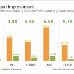
Here’s a chart showing Spectre APS versus Spectre X simulation speeds across six different benchmark circuits, with the same accuracy:

Good news is that you don’t have to wait days for your SPICE results, because with this new speed you can get results in hours, but then again most engineers will just have more desire to run additional simulations that weren’t even possible before. For capacity you should expect to simulate 10’s of millions of active devices and billions of parasitics with Spectre X.

Not only does Spectre X run from the command line, you can also simulate inside of AMS Designer or Virtuoso ADE, even doing RF analysis. The Spectre family of simulators is integrated with many tools across the IC design spectrum.

Summary

The SPICE marketplace now has a new contender that is just as accurate as Spectre, with the added benefits of speed and capacity jumps over Spectre APS, continuing to use the same netlist format, models and output formats. Learning Spectre X should be quite simple for Spectre or APS users, taking just a few minutes, while saving days or weeks by the runtime improvements.

The only question for me is the pricing, and how many tokens it will take to run Spectre X. Talk to your local account manager to get pricing details.

Related Blogs


A Practical Approach to Modeling ESD Protection Devices for Circuit Simulation

A Practical Approach to Modeling ESD Protection Devices for Circuit Simulation
by Tom Simon on 06-03-2019 at 8:00 am

Lurking inside of every Mosfet is a parasitic bipolar junction transistor (BJT). Of course, in normal circuit operation the BJT does not play a role in the device operation. Accordingly, SPICE models for Mosfets do not behave well when the BJT is triggered. However, these models work just fine for most purposes. The one important application where modeling the BJT is important is for electrostatic discharge (ESD) protection circuits. ESD can be a serious threat to product yield and reliability. It is important to model ESD events before chips are fabricated to avoid problems during manufacturing and in the field. ESD events involve higher voltages and currents, that can lead to impact ionization as potential builds up across depleted junctions.

Impact ionization can cause avalanche breakdown effects, where large numbers of electrons are broken loose in an accelerating cycle. The movement of carriers during avalanche breakdown creates a current in the substrate that will trigger the BJT. Under these conditions the device is carrying additional current, creating a positive feedback loop that lowers the voltage across the device while increasing current. This is known as snapback, which wreaks havoc on traditional MOS device models.

After snapback the I-V curve shows an increase in current as voltage is increased, up to the point where there is a second avalanche that leads to thermal breakdown of the device. To properly model a Mosfet when used for an ESD application, the above behaviors must be handled by the model. Empirical data for ESD device performance can be obtained through transmission line pulse (TLP) measurements. The resulting table model is called a TLP model. This can be a useful source of information in creating an accurate SPICE model for an ESD device.

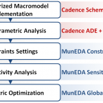
In work done at Brazil based RFID chip maker CEITEC, a macromodel was used to comprehensively model these types of devices. They worked together with MunEDA, who develops analog circuit optimization tools, to simulate and adjust the parameters in the device macromodel so that simulated results matched the measured TLP data. The work is summarized in a presentation titled “Parametric Analysis and Optimization of MOSFET Macromodels for ESD Circuit Simulation” by Robert Dettenborn. The resulting macromodel itself is made up of only standard SPICE elements.

Key steps and tools adopted in the approach

The target process was 180nm CMOS. The first step was to establish a proposed topology for a GGNMOS protection device, which in their case contained a standard Mosfet, a parameterized BJT model and resistors for Rsub and Rgate. For the BJT, a MEXTRAM compact model was used because it is suitable for high current and high voltage operation. It is worth noting that the foundry’s BJT model usually cannot be used because the parasitic device is different than a regular BJT. The presentation goes into the specific differences.

The MULT parameter of MEXTRAM compact model was used to adjust the I-V characteristics so they approximated the measured device. This was done with Cadence ADE and Spectre. The final MULT value used was 70. Further tuning was done to determine the initial value of Rsub. Interestingly, after running parametric analysis, the decision was made to remove Rsub, because the avalanche current values matched better without it. The base resistance model of MEXTRAM was then the sole responsible for the substrate resistance behavior of the macromodel. A drain side resistor, Rd, was added, after which further parametric analysis showed that a good value was around 2 Ohms.

The heavy lifting then started with the optimization of the Mosfet macromodel, including the BSIM4 and MEXTRAM models for the active devices. The MunEDA WiCkeD Constraint Editor was used to implement the initial constraints. MunEDA WiCkeD Sensitivity Analysis was used along with Spectre to determine the influence of each of the initial constraint settings. This was done to ensure that the correct upper and lower limits of the parameters were used in the optimization phase.

MunEDA’s Global Nominal Optimization (GNO) and Deterministic Nominal Optimization (DNO) tools were used to optimize the parameters to fit to the TLP curve. Targets performances were set for Vt1, It1, Vh, Ih, and Vt2, which covers the initial triggering point I-V, the holding point I-V, and the breakdown voltage. In addition, an acceptable upper and lower bound for each performance was specified. GNO also uses several settings to control the algorithm. The number of generations was set to 5, the number of samples for each was set to 10,000 and the sample area for the parameters was set to be equal to the upper and lower limits of variation.

In this case acceptable values were reached after the 5 generations of GNO. If GNO did not yield desirable results, further optimization could be performed with DNO. In this case, MunEDA WiCkeD Sensitivity Analysis along with a Sweep Analysis can be used prior, to ensure that the initial parameter values and optimization boundaries are able to produce target performance results without discontinuities. Once this is done DNO can be run and better optimization results can be achieved.

The paper shows that the final results of this flow give a model that fits the TLP data very well. This opens the door to running traditional SPICE simulations to closely examine ESD protection performance and behavior. This is important because characteristics of the ESD device, such as load capacitance, may adversely affect IO performance. With a SPICE macromodel for the ESD device, simulation tests can be run to verify that the protected devices are not exposed to conditions that can lead to failure or degraded performance.

Simulation vs. TLP results for a GGNMOS protection device

It is only possible to summarize the process here, much more detail is contained in the presentation available on the MunEDA website. MunEDA analog tools can be applied to a wide variety of design problems.  This is just one example of their utility and usefulness.


The Genius Sperm Bank

The Genius Sperm Bank
by John East on 06-03-2019 at 5:00 am

The “20 Questions with John East” series continues

How did it happen?  How did Fairchild transform over a decade into the “off with their heads” culture?  To understand that, you need to know a little about the William Shockley story. William Shockley was born in London in 1910.  He moved to Silicon Valley when he was 3.  Of course, it wasn’t called Silicon Valley then.  There was no silicon in Silicon Valley until he brought it here in 1956.   He was a problem child from the get-go.  He had a terrible temper — generally driving his parents nuts.  But — He was smart!!!  He could count to four before he turned one year old.  In fact, those who knew him later in life generally agreed that he was the smartest person they’d ever met.  He studied at Cal Tech and then did his PhD at MIT.  Then he took a job at Bell Telephone Laboratories in New Jersey.

Shockley built such a reputation for brilliance in his early years at Bell that the government “borrowed” him during World War II to assist in various planning and strategic efforts.  At one time he held the title of Director of Research for the US war efforts.  At the end of the war, he was awarded the National Medal of Merit for contributions made to our war effort even though he had remained, in fact, a civilian throughout the war.

After the war, Shockley returned to Bell Labs where he worked on semiconductor technology with Walter Brattain and John Bardeen.  The concept of a “transistor”  (It hadn’t been named that yet) had existed for several years in people’s minds,  but no one had succeeded in building one.   In 1947, Brattain, Bardeen, and Shockley succeeded.  They built the first functional transistor.  Most of the work, in fact, was done by Bardeen and Brattain, but Shockley was happy to accept most of the credit.  In 1956, the three received a Nobel Prize for their discovery.

In 1956 Shockley decided that he didn’t want to work for a salary any longer.  He reasoned that, with his superior intellect and the head start he had at understanding semiconductors, he should be able to make a fortune by starting his own semiconductor company.  Accordingly he moved to Palo Alto, his old home, and opened Shockley Semiconductor.   He hired the best and the brightest engineers and scientists that he could find (Most of them went on to have fabulous careers) and set out to conquer the semiconductor world.  There was just one problem — in a management role he was an overbearing tyrant.  He drove all of his employees nuts.  Eventually they bailed out.   In particular, a group of eight brilliant engineers lead by Robert Noyce and including Gordon Moore gave notice and left en masse.  Shockley dubbed them the Traitorous Eight.  Because of the mass exodus coupled with a major strategic error (Focusing on 4 layer diodes instead of transistors) Shockley Semiconductor eventually went under.

I met Bill Shockley at Stanford at some time during the 70s.    He was giving a lecture at Stanford that was open to the public. I wish I could remember exactly when the lecture was or what it was about.  I can’t. (I’m sure that it was not about eugenics, though).  After the talk, I waited until the crowd around him had died down.  Then I went up to introduce myself and thank him for creating the business I had already grown so fond of.  — The semiconductor business.   When you shook his hand, you could tell that he had a huge personality.  Clearly physically fit.  Strong grip.  Piercing, direct eye contact.  The usual signs.  I was seven inches taller, 50 pounds heavier, and 35 years younger than Shockley, but I had a pretty clear sense that he was the boss and that, in a fair fight, he could have kicked my ass.

Without question, he was the greatest semiconductor physicist of his time.  Unfortunately for him, though, he couldn’t stick to physics.  He took up eugenics.  He began studying intellectual differences between races.  He preached that the world was suffering from intellectual regression to the mean.  By doing so, he became a hated man.  His views were, in short form, that too many babies were being produced by parents with inferior intellect and not enough by parents of superior intellect.  Luckily (or should I say perversely?) he knew how to solve that problem.  He teamed up with a millionaire eugenicist named Robert Graham to open what was referred to as The Genius Sperm Bank.  Yes.  It really existed.  Officially it was “the Repository for Germinal Choice”

There are many different rumors about the sperm bank, but the most prevalent is that you had to be a Nobel Prize winner in order to be allowed to donate sperm to the Repository.  In any event, it’s certain that Shockley was a donor but uncertain if there were donors other than Shockley.  Rumors have it that Shockley was the only donor.  In fact, Shockley may well have had concerns that the sperm bank’s manufacturing division might not be able to keep up with the demand.  It was clear to Shockley that, once discerning ladies learned that they could choose to bear the child of a Nobel Prize winning genius, they would flock to the Repository and the regression to the mean problem would be solved.  There was just one problem.  They didn’t flock.

Eugenics is not a good subject to proselytize these days.  It wasn’t then either.  The world rapidly turned against him.  He became an outcast, even from his fellow professors at Stanford.  He died of prostate cancer in 1989.  An outcast. Deemed a racist.  A pariah.

But the Traitorous Eight lived on!

See the entire John East series HERE.

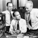
Pictured:  The inventors of the transistor.  From the left: John Bardeen, William Shockley, Walter Brattain.


Needham is Upbeat about EDA and IP Growth at #56DAC

Needham is Upbeat about EDA and IP Growth at #56DAC
by Daniel Payne on 06-02-2019 at 10:42 pm

Wally Rhines, Rich Valera

It’s Sunday afternoon and I just attended the annual Needham presentation at #56DAC in sunny Las Vegas, where Rich Valera shared an upbeat view of EDA and IP growth.  Here are the five drivers of this growth:

  • IoT
  • Automotive
  • Webscale/FAANGs
  • AI/ML
  • China
Rich Valera, Needham (Source: DAC)

For the IoT market they’ve seen a CAGR of 8.6% to $8.2B in 2018, projected to reach $11.4B in 2022.

Auto Semiconductor revenues saw a 6.4% CAGR to 2015, but then a big inflection point happened with a CAGR of 11.1% starting in 2016 (Gartner), with some $34B, projected to reach $69B by 2023. We’re still mostly at Level 2 of ADAS now, which is still a long way from level 5 and autonomy. Yes, Tesla gets too much press attention, but expect several other vendors to be shortly entering the EV market.

FAANGs are these popular companies: Facebook, Apple, Amazon, Netflix, Google. Which just these five companies combined have delivered some 40% of the NASDAQ increase over the past 5 year time period. All of these companies are doing some HW designs. Remember that Apple purchased PA Semi in 2008 to start designing their own processors, and now their A-series of chips power the iPhone, iPad and iWatch products.

Amazon bought Annapurna in 2016 to help bolster AWS.

Google in 2016 announced their new chip, the TPU, and second generation coming out, helping bolster their AI initiatives.

Facebook surprisingly Bought Sonics for their interconnect IP,  which will help on  VR and AR applications.

AI/ML is the number one driver in new EDA licenses, where in 2017 some $7B in revenue was generated, growing by 2020 to $32B, and projected in 2025 to reach $65B. CPU and GPU approaches were initially used for AI/ML, but now the big shift is towards custom silicon, aka ASIC. Yes, there are too many AI startups now getting VC, so it’s likely that most will not be successful. During a SNPS conference call it was learned that some 200 AI chip projects are underway, so yes, this is driving new ASIC starts.

China is still in growth mode for EDA tools and IP, as Cadence shows that 10% of their revenue now comes from China. There are big concerns about Huawei, because they were placed on the USA entity list, so American companies cannot sell new software or IP into that company.

EDA and IP revenue growth rate by quarter show that in Q4 2018 it was shrinking to under a 5% annualized rate, although there are some wonky numbers that make up that Q4 2018 amount.

IPO activity has been quite good in the early years from 1996 through 2002, but in the period from 2002 to 2018 we mostly saw consolidation, without any new IPOs. Investors have not been as attracted to EDA growth rates, so maybe they don’t see enough scale happening.

The R&D spending levels of SNPS and CDN are about 35% of revenue, so that is still a big investment, maybe too much R&D compared to other industries. In the SW and Semi industries we see about a 25% R&D investment level.

Stock growth has been outstanding for EDA companies in the past five years: CDN (360% over 5 years), SNPS, ANSS (245%), NASDAQ (laggard).

Wally Rhines, Rich Valera

Summary
EDA and semiconductor IP revenues have a healthy growth, driven by factors like: Automotive electrification, IoT, FAANG, AI/ML, China growth. We expect

Q&A

Q: What about 5G?
A: Good question, there’s lots of hype on 5G, but not much capex expected from major carriers, so we expect a gentle upgrade cycle.

Q: Any comments on growth from Defense or DARPA areas?
A: Not that much change over time as growth, no.

Q: Are you tracking open source EDA and IP trends?
A: No, not yet.

Q: Will China develop their own EDA tools?
A: Yes, they are trying to catch up. Although their fabs are not leading edge yet.


In Their Own Words: TSMC and Open Innovation Platform

In Their Own Words: TSMC and Open Innovation Platform
by Daniel Nenni on 06-01-2019 at 8:00 am

TSMC, the largest and most influential pure-play foundry, has many fascinating stories to tell. In this section, TSMC covers some of their basic history, and explains how creating an ecosystem of partners has been key to their success, and to the growth of the semiconductor industry.

The history of TSMC and its Open Innovation Platform (OIP)® is, like almost everything in semiconductors, driven by the economics of semiconductor manufacturing. Of course, ICs started 50 years ago at Fairchild (very close to where Google is headquartered today, these things go in circles). The planarization approach, whereby a wafer (just 1” originally) went through each process step as a whole, led to mass production. Other companies such as Intel, National, Texas Instruments and AMD soon followed and started the era of the Integrated Device Manufacturer (although we didn’t call them that back then, we just called them semiconductor companies).

The next step was the invention of ASICs with LSI Logic and VLSI Technology as the pioneers. This was the first step of separating design from manufacturing. Although the physical design was still done by the semiconductor company, the concept was executed by the system company. Perhaps the most important aspect of this change was not that part of the design was done at the system company, but rather the idea for the design and the responsibility for using it to build a successful business rested with the system company, whereas IDMs still had the “if we build it they will come” approach, with a catalog of standard parts.

In 1987, TSMC was founded and the separation between manufacture and design was complete. One missing piece of the puzzle was good physical design tools and Cadence was created in 1988 from the merger of SDA and ECAD (and soon after, Tangent). Cadence was the only supplier of design tools for physical place and route at the time. It was now possible for a system company to buy design tools, design their own chip and have TSMC manufacture it. The system company was completely responsible for the concept, the design, and selling the end-product (either the chip itself or a system containing it). TSMC was completely responsible for the manufacturing (usually including test, packaging and logistics too).

At the time, the interface between the foundry and the design group was fairly simple. The foundry would produce design rules and SPICE parameters for the designers; the design would be given back to the foundry as a GDSII file and a test program. Basic standard cells were required, and these were available on the open market from companies like Artisan, or some groups would design their own. Eventually TSMC would supply standard cells, either designed in-house or from Artisan or other library vendors (bearing an underlining royalty model transparent to end users). However, as manufacturing complexity grew, the gap between manufacturing and design grew too. This caused a big problem for TSMC: there was a lag from when TSMC wanted to get designs into high volume manufacturing and when the design groups were ready to tape out. Since a huge part of the cost of a fab is depreciation on the building and the equipment, which is largely fixed, this was a problem that needed to be addressed.

At 65 nm TSMC started the Open Innovation Platform (OIP) program. It began at a relatively small scale but from 65 nm to 40 nm to 28 nm the amount of manpower involved went up by a factor of 7. By 16 nm FinFET, half of the design effort is IP qualification and physical design because IP is used so extensively in modern SoCs, OIP actively collaborated with EDA and IP vendors early in the life-cycle of each

process to ensure that design flows and critical IP were ready early. In this way, designs would tape-out just in time as the fab was starting to ramp, so that the demand for wafers was well-matched with the supply.

In some ways the industry has gone a full circle, with the foundry and the design ecosystem together operating as a virtual IDM. The existence of TSMC’s OIP program further sped up disaggregation of the semiconductor supply chain. Partly, this was enabled by the existence of a healthy EDA industry and an increasingly healthy IP industry. As chip designs had grown more complex and entered the SoC era, the amount of IP on each chip was beyond the capability or the desire of each design group to create. But, especially in a new process, EDA and IP qualification was a problem.

On the EDA side, each new process came with some new discontinuous requirements that required more than just expanding the capacity and speed of the tools to keep up with increasing design size. Strained silicon, high-K metal gate, double patterning and FinFETs each require new support in the tools and designs to drive the development and test of the innovative technology.

On the IP side, design groups increasingly wanted to focus all their efforts on parts of their chip that differentiated them from their competition, and not on re-designing standard interfaces. But that meant that IP companies needed to create the standard interfaces and have them validated in silicon much earlier than before.

The result of OIP has been to create an ecosystem of EDA and IP companies, along with TSMC’s manufacturing, to speed up innovation everywhere. Because EDA and IP groups need to start work before everything about the process is ready and stable, the OIP ecosystem requires a high level of cooperation and trust.

When TSMC was founded in 1987, it really created two industries. The first, obviously, is the foundry industry that TSMC pioneered before others entered. The second was the fabless semiconductor companies that do not need to invest in fabs. This has been so successful that two of the top 10 semiconductor companies, Qualcomm and Broadcom, are fabless and all the top FPGA companies are fabless.

The foundry/fabless model largely replaced IDMs and ASIC. An ecosystem of co-operating specialist companies innovates fast. The old model of having process, design tools and IP all integrated under one roof has largely disappeared, along with the “not invented here” syndrome that slowed progress since ideas from outside the IDMs had a tough time penetrating. Even some of the earliest IDMs from the “Real men have fabs” era have gone “fab lite” and use foundries for some of their capacity, typically at the most advanced nodes.

Legendary TSMC Chairman Morris Chang’s “Grand Alliance” is a business model innovation of which OIP is an important part, gathering all the significant players together to support customers—not just EDA and IP, but also equipment and materials suppliers, especially for high-end lithography.

Digging down another level into OIP, there are several important components that allow TSMC to coordinate the design ecosystem for their customers.

  • EDA: the commercial design tool business flourished when designs got too large for hand-crafted approaches and most semiconductor companies realized they did not have the expertise or resources in-house to develop all their own tools. This was driven more strongly in the front-end with the invention of ASIC, especially gate-arrays; and then in the back end with the invention of
  • IP: this used to be a niche business with a mixed reputation, but now is very important with companies like ARM, Imagination, CEVA, Cadence, and Synopsys, all carrying portfolios of important IP such as microprocessors, DDRx, Ethernet, flash memory and so on. In fact, large SoCs now contain over 50% and sometimes as much as 80% TSMC has well over 5,500 qualified IP blocks for customers.
  • Services: design services and other value-chain services calibrated with TSMC process technology helps customers maximize efficiency and profit, getting designs into high volume production rapidly
  • Investment: TSMC and its customers invest over $12 billion a year. TSMC and its OIP partners alone invest over $1.5 billion. On advanced lithography, TSMC has further invested $1.3 billion in

Processes are continuing to get more advanced and complex, and the size of a fab that is economical also continues to increase. This means that collaboration needs to increase as the only way to both keep costs in check and ensure that all the pieces required for a successful design are ready just when they are needed.

TSMC has been building an increasingly rich ecosystem for over 25 years and feedback from partners is that they see benefits sooner and more consistently than when dealing with other foundries. Success comes from integrating usage, business models, technology and the OIP ecosystem so that everyone succeeds. There are a lot of moving parts that all have to be ready. It is not possible to design a modern SoC without design tools, more and more SoCs involve more and more 3rd party IP, and, at the heart of it all, the process and the manufacturing ramp with its associated yield learning all needs to be in place at TSMC.

The proof is in the numbers. Fabless growth in 2013 is forecasted to be 9%, over twice the increase in the overall industry at 4%. Fabless has doubled in size as a percentage of the semiconductor market from 8% to 16% during a period when the growth in the overall semiconductor market has been unimpressive. TSMC’s contribution to semiconductor revenue grew from 10% to 17% over the same period.

The OIP ecosystem has been a key pillar in enabling this sea change in the semiconductor industry.

TSMC 2019 Update

2019 TSMC Technology Symposium Review Part I

TSMC Technology Symposium Review Part II


Global Unichip Corporation

Another facet of TSMC is GUC, Global Unichip Corporation. It is a partially owned subsidiary and also an important partner, providing design services and allowing TSMC themselves to continue to be a pure-play foundry. GUC was founded in 1998 with 10 employees as what has come to be known as a “Design Service” company. It ramped fast and by 2000 it employed over 100 people.

The years between 2003 and 2010 were milestone years for GUC, representing a period of unprecedented growth. The era was marked by a strengthening of both business and technology relationships with the largest semiconductor foundry in the world, TSMC. That relationship set GUC on firm growth, bringing over the core of today’s management and the business strategy that guides the company today.

In 2003, TSMC assumed an ownership stake in GUC. But the foundry leader’s investment went far beyond financial investment. Part of its strategy to enhance the return on its investment was to move GUC to a global business strategy and put it on the road to being an advanced technology leader.

The technology model, and the business model that accompanied it, soon began to gain traction. Prior to 2003, much of GUC’s business came from the consumer electronics companies who tended to utilize more mature technologies and were primarily located in Taiwan. With the installation of new management, and new business and technology models, business emphasis began to migrate to the more technically sophisticated networking and communications sectors that required more advanced technologies. In 2004, 100% of GUC’s revenue was at  the 0.13 µm technology node; by 2005, 5% of revenue came from the new 90 nm node and a year later, an additional 3% of revenue came from the emerging 65 nm node.

The impact of this trend was soon seen in the company finances. Revenue jumped from $20 million in 2002 to $27 million in 2003, $32 million in 2004, and a whopping $48 million in 2005—more than doubling the revenue over a four year period.

The year 2006 marked another major milestone. In the third quarter of that year, GUC became a publicly traded company when it offered its shares on the Taiwan Stock Exchange.

The operations side instituted a major focus on advanced technology. In 2007, the company developed an advanced technology digital design flow, followed shortly thereafter by a low power design flow. As a result, the company saw a large increase in the size of their designs, many with gate counts jumping exponentially. In the face of an industry-wide recession in 2009, GUC showed its confidence in the future by investing heavily in internal IP development, in particular, IP targeting the networking market segment.

This era of prosperity was reflected by a broad set of indices. Annual revenue in 2006 more than doubled that of 2005 ($48 million) at $103 million, then more than doubled again in 2007 to $216 million. In 2008, revenue jumped to $295 million before falling during the recession of 2009 to $252 million. In 2008, GUC saw a jump in revenue from advanced technology to 21 % and to 34 % in 2009, with 1 % of that coming from leading edge 40 nm products. Like all technology companies, GUC experienced a financial decline in 2009, with revenues dropping to $252 million.

But the company would rebound quickly in 2010, posting revenues of $327 million with advanced technologies accounting for 42% of that total. The year also proved auspicious. Driven by the recession to examine its business model, GUC would begin making a series of strategic decisions that would allow it to capitalize on a new era of semiconductor device design.

The company’s growth as an innovative force in the semiconductor industry is also reflected in the number of new employees required to implement increasingly complex technologies. At the end of 2003, GUC employed 132 people, most of them in Taiwan. Three years later, that number had more than doubled to 287 and by the start of 2010, the company counted 484 employees, a number that has held relatively steady through 2013. Employee growth was fueled by expanded geographic growth. GUC opened its first international office when it established a subsidiary in North America (GUC N.A.) in February of 2004 and then opened its Japan office in June of 2005. Nearly three years later, in May of 2008, the company opened its third international office, GUC Europe, in Amsterdam, The Netherlands and one month later opened an office in Korea. GUC entered the fast-growing China market when it opened an office in one of that country’s technology hubs near Shanghai in 2009.

Success in the semiconductor industry going forward is going to be heavily weighted by the ability to leverage industry’s third-party infrastructure that has now matured. Foundries are at the leading edge of the infrastructure, providing the most advanced process technologies, as well as specialized technologies to all comers. IP and chip design implementation are also being outsourced, cost-effectively utilizing technology and financial resources.

It is in this new and exciting environment that GUC evolved the Flexible ASIC Model, which is designed to provide the most effective, efficient and flexible path to semiconductor innovation.

The Flexible ASIC Model is a response to both the business and technical challenges facing today’s semiconductor companies. This model allows companies to allocate their resources more efficiently. It brings together design expertise, systems knowledge and manufacturing resources to efficiently drive delivery of the final packaged IC. The model’s basic strategy is to spread design risks and to minimize IDM, fabless and OEM (Original Equipment Manufacturers) upfront semiconductor-related fiscal and human capital investments. The goal is to increase the efficiency of the entire value chain, from concept to delivery; to shorten all phases of the development cycle; and to ultimately increase device yield quality and reliability.

At the heart of the Flexible ASIC Model is integrated manufacturing. GUC has made a strategic choice to work exclusively with TSMC, the semiconductor industry’s leading foundry service company. It is this relationship that plays an integral role in the company’s ability to achieve early advanced technology access and match designs to manufacturing resources.

Spotlight: Dr. Morris Chang

Dell changed the way personal computers are manufactured and sold. Starbucks changed the amount we would pay for a cup of coffee. eBay took the yard sale out of our yards. TSMC took the semiconductor manufacturing costs off our balance sheets and out of our capital investments.

It’s hard to overstate the impact that Dr. Morris Chang, Founder, Chairman, and until-recently CEO of TSMC, has had on the industry. He has been influential as a leader in business model innovation, and has earned his company roughly 50% of the foundry market share.

Chang left his native China in 1949, moving to the US to attend Harvard University. He soon transferred to MIT as he followed his interest in technology. After earning his MS in 1953 from MIT’s mechanical engineering graduate school, Morris went directly into the semiconductor industry at the process level with Sylvania Semiconductor and was quickly moved to management.

Chang moved to Texas Instruments in 1958, where he stayed for 25 years, rising to VP of the worldwide semiconductor business (and also earned a PhD in electrical engineering from Stanford in 1964). At TI, he worked on a four transistor project in which the manufacturing was done by IBM, thus engaging in one of the early semiconductor-foundry relationships. Also at TI, Chang developed a new model of semiconductor pricing that sacrificed early profits to gain market share and to achieve manufacturing yields that would lead to higher long-term profits.

Chang left TI in 1983 and did a short stint at General Instrument Corporation. He then moved to Taiwan to head the Industrial Technology Research Institute (ITRI), which led to the founding of TSMC.

Chang noticed in the early 1980s, while at TI and GI, that top engineers were leaving and forming their own semiconductor companies. Unfortunately, the heavy capital requirement of semiconductor manufacturing was a gating factor. The cost back then was $5-10 million to start a semiconductor company without manufacturing and $50-100 million to start a semiconductor company with manufacturing. Some of these start-ups used excess capacity from IDMs but were subjected to uncertainties in foundry capacity and sometimes had to buy wafers from a competitor. Around this time, 1985, the first truly fabless startups, like Xilinx and Chips and Technologies, were launched and doing well.

It was in 1987, within this nascent fabless environment, that Chang started TSMC. Although TSMC started two process nodes behind where semiconductor manufacturers (IDMs) were at the time, they had the advantage of being a pure-play foundry, not a competitor. Their focus was on their customers.

Morris Chang made the first TSMC sales calls with a single brochure: TSMC Core Values: Integrity, Commitment, Innovation, Partnership. Four or five years later, TSMC was only behind by one process node and the orders started pouring in. In 10 years, TSMC caught up with IDMs (except for Intel) and the fabless semiconductor industry blossomed, enabling a whole new era of semiconductor design and manufacturing. In the last 20 years, and still today, even the remaining IDMs are being forced to go fabless or fab-lite at 28 nm and below due to high costs and daunting technical challenges.

Dr. Morris Chang in 2007.

Dr. Morris Chang turned 82 on July 10th, 2013. He is still running TSMC full time as the founding Chairman. He works from 8:30 am to 6:30 pm like most TSMC employees and says that a successful company life cycle is: rapid expansion, a period of consolidation, and maturity. The same could be said about Chang himself.

2019 Update: Dr. Morris Chang

In 2017 the TSMC Museum of Innovation opened Under Fab 12 in Hsinchu Taiwan. It not only commemorates the history of semiconductors and TSMC but also the life of Dr. Morris Chang. Morris Chang’s wife Sophie was actively involved in this project:

The TSMC Museum of Innovation encompasses three exhibition galleries: “A World of Innovation,” “Unleashing Innovation,” and “Dr. Morris Chang, TSMC Founder.” Through interactive technology, digital content, and historical documents we will learn about the pervasiveness of ICs in our daily lives and about their continued advancement. In addition, we will learn how ICs are making our lives more fulfilling and how they are driving technology beyond our imagination. We will also learn how TSMC contributes to global IC innovation and to Taiwan’s economy.

In 2018 Dr. Morris Chang retired from TSMC for the second and final time:

TSMC Dr. Morris Chang Announces Retirement in June 2018. Future Dual Leadership Will Be Mark Liu as Chairman And C.C. Wei as CEO.

Issued by: TSMC Issued on: 2017/10/02

Hsinchu, Taiwan, R.O.C. – Oct. 2, 2017 – TSMC Chairman Morris Chang today announces: “I will retire from the Company immediately after the Annual Shareholders Meeting in early June, 2018. I will not be a director in the next term of the board of directors. Nor will I participate in any TSMC management activities after the Annual Shareholders Meeting in early June, 2018. From early June, 2018 on, TSMC will be under the dual leadership of Dr. Mark Liu and Dr. C.C. Wei. Dr. Mark Liu will be the Chairman of the Board, and Dr. C.C. Wei will be the Chief Executive Officer. All present directors of the board have agreed to be nominated, and if elected, serve as directors of the board during the next term. They have also agreed to support the aforementioned dual leadership of the Company under Drs. Liu and Wei. Chairman Morris Chang further said, “The past 30-odd years, during which I founded and devoted myself to TSMC, have been an extraordinarily exciting and happy phase of my life. Now, I want to reserve my remaining years for myself and my family. Mark and CC have been Co-CEO’s of the Company since 2013 and have performed outstandingly. After my retirement, with the continued supervision and support of an essentially unchanged board, and under the dual leadership of Mark and CC, I am confident that TSMC will continue to perform exceptionally.”



In Their Own Words: eSilicon Corporation

In Their Own Words: eSilicon Corporation
by Daniel Nenni on 06-01-2019 at 8:00 am

eSilicon was one of the first companies to focus on making the benefits of the fabless semiconductor movement available to a broader range of customers and markets. The company is credited with the creation of the fabless ASIC model. In this section, eSilicon shares some of its history and provides its view of the ever-changing fabless business model.

eSilicon Corporation was founded in 2000 with Jack Harding as the founding CEO and Seth Neiman of Crosspoint Venture Partners as the first venture investor and outside board member. They both remain involved in the company today, with Harding continuing as CEO and Neiman now serving as Chairman of the Board.

Both Harding and Neiman brought important and complementary skills to eSilicon that helped the company maneuver through some very challenging times. Prior to eSilicon, Harding was President and CEO of Cadence Design Systems, at the time the largest EDA supplier in the industry. He assumed the leadership role at Cadence after its acquisition of Cooper and Chyan Technology (CCT), where Harding was CEO. Prior to CCT, Harding served as Executive Vice President of Zycad Corporation, a specialty EDA hardware supplier. He began his career at IBM.

Seth Neiman is Co-Managing Partner at Crosspoint Venture Partners, where he has been an active investor since 1994. Neiman’s investments include Brocade, Foundry, Juniper and Avanex among many others. Prior to joining Crosspoint, Neiman was an engineering and strategic product executive at a number of successful startups including Dahlgren Control Systems, Coactive Computing, and the TOPS division of Sun Microsystems. Neiman was the lead investor in eSilicon and incubated the company with Jack at the dawn of the Pleistocene epoch.

The Early Years

eSilicon’s original vision was to develop an online environment where members of the globally disaggregated fabless semiconductor supply chain could collaborate with end customers looking to re-aggregate their services. The idea was straight-forward—bring semiconductor suppliers and consumers together and use the global reach of the Internet to facilitate a marketplace where consumers could configure a supply chain online. The resultant offering would simplify access to complex technology and reduce the risk associated with complex design decisions. Many fabless enterprises had struggled with these issues, taking weeks to months to develop a complete plan for the implementation of a new custom chip. Chip die size and cost estimates were difficult to develop, technology choices were varied and somewhat confusing, and contractual commitments from supply chain members took many iterations and often required a team of lawyers to complete.

The original vision was simple, elegant and sorely needed. However, it proved to be anything but simple to implement. In the very early days of the company’s existence, two things happened that caused a shift in strategy. First, a close look at the technical solutions required to create a truly automated marketplace yielded significant challenges. Soon after the formation of the company, eSilicon hired a group of very talented individuals who did their original research and development work at Bell Labs. This team had broad knowledge of all aspects of semiconductor design. It was this team’s detailed analysis that lead to a better understanding of the challenges that were ahead.

Second, a worldwide collapse of the Internet economy occurred soon after the company was founded. The “bursting” of the Internet bubble created substantial chaos for many companies. For eSilicon, it meant that a reliable way to monetize its vision would be challenging, even if the company could solve the substantial technical issues it faced. As a result, most of the original vision was put on the shelf. The complete realization of the “e” in eSilicon would have to wait for another day. All was not lost in the transition, however. Business process automation and worldwide supply chain relationships did foster the development of a unique information backbone that the company leverages even today. More on that later.

The Fabless ASIC Model

Mounting technical challenges and an economic collapse of the target market have killed many companies. Things didn’t turn out that way at eSilicon. Thanks to a very strong early team, visionary leadership and a little luck, the company was able to redirect its efforts into a new, mainstream business model. It was clear from the beginning that re-aggregating the worldwide semiconductor supply chain was going to require a broad range of skills. Certainly, design skills would be needed. But back-end manufacturing knowledge was also going to be critical. Everything from package design, test program development, early prototype validation, volume manufacturing ramp, yield optimization, life testing, and failure analysis would be needed to deliver a complete solution. Relationships with all the supply chain members would be required and that took a special kind of person with a special kind of network.

eSilicon assembled all these skill sets. That deep domain expertise and broad supply chain network allowed the company to pioneer the fabless ASIC model. The concept was simple—provide the complete, design-to-manufacturing services provided by the current conventional ASIC suppliers, such as LSI Logic, but do it by leveraging a global and outsourced supply chain. Customers would no longer be limited to the fab that their ASIC supplier owned, or their cell libraries and design methodology.

Instead, a supply chain could be configured that optimally served the customer’s needs. And eSilicon’s design and manufacturing skills and supply chain network would deliver the final chip. The volume purchasing leverage that eSilicon would build, coupled with the significant learning eSilicon would achieve by addressing advanced design and manufacturing problems on a daily basis would create a best-in-class experience for eSilicon’s customers.

eSilicon’s positioning, DAC 2000

As the company launched in the fall of 2000, the fabless ASIC segment of the semiconductor market was born. Gartner/ Dataquest began coverage of this new and growing business segment. Many new fabless ASIC companies followed. Antara.net was eSilicon’s first customer. The company produced a custom chip that would generate real-world network traffic to allow stress-testing of e-business sites before they went live. Technology nodes were in the 180 nm to 130 nm range and between eSilicon’s launch in 2000 and 2004, 37 designs were taped out and over 14 million chips were shipped.

Fabless ASIC was an adequate description for the business model as everyone knew what an ASIC was, but the description fell short. A managed outsourced model could be applied to many chip projects, both standard and custom. As a result, eSilicon coined the term Vertical Service Provider (VSP), and that term was used during the company’s initial public exposure at the Design Automation Conference (DAC) in 2000.

The model worked. eSilicon achieved a fair amount of notoriety in the early days as the supplier of the system chip that powered the original iPod for Apple. The company also provided silicon for 2Wire, a company that delivered residential Internet gateways and associated services for providers such as AT&T. But it wasn’t only the delivery of “rock star” silicon that set the company apart; some of the original e-business vision of eSilicon did survive.

The company launched a work-in-process (WIP) management and logistics tracking system dubbed eSilicon Access® during its first few years. The company received a total of four patents for this technology between 2004 and 2010. eSilicon Access, for the first time, put the worldwide supply chain on the desktop of all eSilicon’s customers. Using this system, any customer could determine the status of its orders in the manufacturing process and receive alerts when the status changed. eSilicon uses this same technology to automate its internal business operations today.

Growing the Business

During the next phase of growth for the company, from 2005 to 2009, an additional 135 designs were taped out and an additional 30 million chips were shipped. Technology nodes now ranged mainly from 90 nm down to 40 nm. It was during this time that the company began expanding beyond US operations. Through the acquisition of Sycon Design, Inc., the company established a design center in Bucharest, Romania. A production operations center was also opened shortly thereafter in Shanghai, China.

Recognizing the growing popularity of outsourcing, eSilicon expanded the VSP model to include semiconductor manufacturing services (SMS). SMS allowed fabless chip and OEM companies to transition the management of existing chip production or the ramp-up and management of new chip production to eSilicon. The traditional design handoff of the ASIC model was now expanded to support manufacturing handoff. The benefits of SMS included a reduction in overhead for the customer as well as the ability to focus more resources on advanced product development. Extensions such as SMS caused the Vertical Service Provider model to expand, creating the Value Chain Producer (VCP) model. The Global Semiconductor Alliance (GSA) recognized the significance of this new model and elected Jack Harding to their Board to represent the VCP segment of the fabless industry.

In the years that followed, up to the present day, eSilicon has grown substantially. The number of tape-outs the company has achieved is now approaching 300 and the number of chips shipped is on its way to 200 million. The company has also expanded into the semiconductor IP space. While its worldwide relationships for third-party semiconductor IP are critical to eSilicon’s success, the company recognized that the ability to deliver specific, targeted forms of differentiating IP could significantly improve the customer experience.

eSilicon’s first logo. The squares symbolize the end product—the chip.

Since so many of today’s advanced chip designs contain substantial amounts of on-board memory, this is the area that was chosen for eSilicon’s initial IP focus. The company acquired Silicon Design Solutions, a custom memory IP provider with operations in Ho Chi Minh City and Da Nang, Vietnam. This acquisition added 150 engineers to focus on custom memory solutions for eSilicon’s customers.

As of June 30, 2013, eSilicon employs over 420 full-time people worldwide, of which over 350 are dedicated to engineering. Headquartered in San Jose, California, the company maintains operations in New Providence, New Jersey and Allentown, Pennsylvania; Shanghai, China; Seoul, South Korea; Bucharest, Romania; Singapore and Ho Chi Minh City and Da Nang, Vietnam. The company’s diverse global customer base consists of fabless semiconductor companies, integrated device manufacturers, original equipment manufacturers and wafer foundries. eSilicon sells through both an internal sales force and a network of representatives.

The Evolving Model

The eSilicon business model has evolved further. VSP and VCP are now SDMS (semiconductor design and manufacturing services). Arguably the longest, but perhaps the most intuitive name. Through the years, Silicon has allowed a broad range of companies to reap the benefits of the fabless semiconductor model, many of which couldn’t have done it on their own.

eSilicon’s current logo. The three “S” graphic symbolized the process and culture—speed, simplicity, and self-confidence.

This ability to bring a worldwide supply chain within reach to smaller companies gave eSilicon its start, but the model has worked well for eSilicon beyond these boundaries. Today, eSilicon serves customers that are much larger than eSilicon itself; customers that could “do what eSilicon does.” In the early days, the company discounted its chances of winning business at an enterprise big enough to maintain an “eSilicon inside.”

Time has proven this early thinking to be too limiting. Many of eSilicon’s customers today can clearly maintain an “eSilicon inside,” but they still rely on eSilicon to deliver their chips. Why? In two words, opportunity cost. It has been proven over time that for any enterprise the winning strategy is to focus on the organization’s core competence and invest in that. All other functions should be outsourced in the most reliable and cost-effective manner possible. Simply put, eSilicon’s core competency fits in the outsourcing sweet spot for many, many organizations. This trend has created new value in the fabless semiconductor sector and facilitated many new design starts.

What’s Next?

As the fabless model grows, there are new horizons emerging. During its early days, the vision of using the Internet to facilitate fabless technology access and reduce risk was largely put on the shelf. The reasons included the challenges of solving complex design and manufacturing problems and the lack of a clear delivery mechanism over the Web.

Today, these parameters are changing. The Internet is now an accepted delivery vehicle for a wide array of complex business-to-business solutions. eSilicon’s talented engineering team has also developed a substantial cloud-enabled environment that is used to automate its internal design and manufacturing operations every day. This team consists of many of the same people who highlighted the challenges of addressing these issues in the company’s early years. What a difference a decade can make.

What if that automated environment could be made available to end users in a simple, intuitive way? New work at eSilicon is taking the company in this direction. The recent announcement of an easy-to-use multi-project wafer quote system is an example. What once could take two weeks or more, consisting of many inquiries and legal agreement reviews, is now done in as little as five minutes with an extension to eSilicon Access. With availability on both the customer’s desktop and smartphone, this is clearly the beginning of a new path. eSilicon changed the landscape of fabless semiconductor in 2000 with the introduction of the fabless ASIC model. It’s time to do it again and bring back the “e” in eSilicon.

2019 Update: eSilicon Corporation

A lot has happened since 2013. Some “ups”, some “downs”, a lot of innovation and some surprises as well. The story told here applies to the industry in general, not just eSilicon.

We ended the original chapter on eSilicon talking about the potential to put the “e” back in eSilicon, leveraging an internet-based business model. That did indeed happen, but there’s so much more to the story.

In our previous closing remarks, we talked about an easy-to-use multi-project wafer (MPW) quoting system. By way of explanation, an MPW is essentially a cost-sharing strategy. Rather than one customer paying the full cost of a mask set and prototype manufacturing run, what if the mask could contain designs from many customers? Each customer would then get a pre-determined number of chips from the prototype run and the cost would be split among all participants. This strategy dramatically reduces the cost of building a prototype of a new silicon idea.

Our online MPW quoting system held the promise of collapsing a two-week fact-finding mission into a five-minute, fill-in-the-blanks quote generation experience. We did deliver that experience, and a lot more. It is interesting to note that, while the semiconductor industry essentially created the internet, the people who work in the semiconductor industry aren’t all that interested in using the internet for their business.

Our online MPW quoting system met with lackluster interest. Except for university researchers. It turns out this is where the customers were. Semiconductor research only becomes relevant when it’s proven in silicon. To achieve that goal, university researchers need to implement their design with a low-cost MPW run. University professors and their students are big fans of the internet, and so our online MPW quoting system was a hit with them. We began to build a worldwide user base for the tool. By January, 2017 we had approximately 1,500 users of our online MPW quoting tool in over 50 countries. We also added a lot more automation beyond quoting.

Prior to our online automation, it took six signatures to implement an MPW run. Uploading the final design could take three days and running final design rule checks could take even more time. When fully deployed, the system required zero signatures and final designs could be instantly uploaded and a design rule check would be automatically run with results sent back to the researcher in hours. We branded the online platform STAR, which stood for self-service, transparent, accurate and real-time. These are the words we always used to describe the system, so we “went with the flow.” We also took the opportunity to do a re-brand of the company. Essentially update our image to reflect the new, online nature of our business.

Those who work in marketing will appreciate this next point. We commissioned a new logo design. Why? Not because we didn’t like the old logo or the three “S” symbology for speed, simplicity, and self-confidence. We liked all that just fine. The problem was that the original logo was designed in a time when print media dominated the communication agenda. The graceful three “S” graphic was quite stunning in high-resolution print, but the detailed graphic elements were not well-suited to digital media. So, we created a new logo that maintained the message but was digital friendly.

We added much more automation technology to our STAR platform as well. The business, while small, was doubling year on year, with the promise to grow even faster, as online businesses tend to do. In January, 2017, we decided to shut down our online MPW business. The reasons for such a radical decision require turning the page to the next chapter of eSilicon and the ASIC business.

While our online business began around 2013, another trend began to take shape around that time. The trend of consolidation in the semiconductor industry. It began slowly at first but picked up steam along the way. LSI Logic was bought by Avago. Then Emulex and few more. And then Broadcom. What was once a focused, flexible top-end ASIC company was now part of a massive, worldwide standard product enterprise. During this same time, the mighty IBM Microelectronics, one of the major players in the top-end of the ASIC market along with LSI Logic, became part of GLOBALFOUNDRIES. There was more consolidation during this time across the world.

The result of this macro trend was the creation of a “hole” in the top end of the ASIC market. The companies that previously addressed this segment were now part of larger enterprises. ASIC was a part of the equation, but not the complete picture anymore. And these larger enterprises tended to compete with their ASIC customers due to their large standard product footprint.
Pure-play ASIC companies to address the needs of the top-end of the market were needed. And eSilicon had the right profile to address these needs. So, in January, 2017 eSilicon’s management team assembled for a strategic planning session. Many options to blend our various businesses were weighed, but one simple analysis, drawn on the whiteboard by our CFO, drove the point home.

Our online business was a good one, but it didn’t fit with the dynamics of our new opportunity to serve the top-end of the ASIC market—a substantial and lucrative opportunity. So, we shut down our online business. Between January and May of 2017, we did a record number of MPW tape-outs and then we moved on.

The next chapter in eSilicon’s history has been quite exciting. It began with one design win in the top-end of the ASIC market and then another and more after that. Today, eSilicon focuses most of its energy serving this market for the high-performance networking, computing, 5G infrastructure, and AI segments. We’ve developed a substantial array of differentiating semiconductor IP to address the unique needs of these markets. While this shift is significant for eSilicon, there is a bigger shift happening that is relevant for the entire ASIC market.

That shift has to do with what we’ll call ASIC success. When the first version of this book was published, ASIC success meant handing off a chip to the end customer that passed the manufacturing test program. Given the levels of complexity and integration delivered by those designs, this model worked. Today, it’s different. At the top end of the market, it’s often not a chip that’s delivered by the ASIC vendor. Instead, it’s a highly complex system-in-a-package that typically contains a massive, FinFET-class chip and multiple 3D memory stacks integrated on a silicon interposer.

Passing the manufacturing test program is just the beginning of bringing up a design like this in the target system. There are chip/package/system interactions, the need to debug potential interactions between semiconductor IP from multiple sources and hardware/software/firmware interactions. In this environment, delivering the required performance of the chip in the system context is the new measure of success. The task is daunting, but rewarding. Hitting the mark on a new router or 5G infrastructure component is quite lucrative for all involved. Getting there isn’t easy, but clearly worth it.

In this new paradigm of what ASIC success means, eSilicon finds itself playing the role of coordinator for multiple supply chain partners. The goal of delivering the required ASIC performance in the system context does take a lot of companies and a lot of coordination. It’s common in this new world to have ALL departments involved in a design kick-off meeting. System, chip, package, test, firmware and quality all have a role to play, and all have to work in a coordinated fashion from the very beginning to stay ahead of the curve. It’s also typical to assemble the bring-up team at the customer months before the chip is out of fab to plan all the hardware/software/firmware/package interactions required to achieve ASIC success.

The systems that these new ASICs power will, undoubtedly, change the world. eSilicon is proud to be part of the revolution.


Ten Things to see @ 56th DAC!

Ten Things to see @ 56th DAC!
by Daniel Nenni on 06-01-2019 at 8:00 am

New products always take precedence since EDA is a “mature” market. I have inside knowledge on this one so I can tell you it is not to be missed. Coincidently, but not really, a related white paper was just published so if you are not going to 56thDAC you can still get a virtual briefing. If you are going to DAC be sure and stop by the Fractal booth #561 to get a demo.

New Product: IP Delta QA

Associated white paper Why IP sign-off is not enough

EDA in the Cloud

It has finally happened, EDA is actually in the cloud and the results are incredible. SemiWiki is also in the cloud and as I sit at the Google Cloud Platform control panel I realize that all of the cloud talk in the past barely scratched the surface of what can be done. We are now seeing actual chip design case studies versus marketing hyperbole and DAC is the place for it, absolutely.

There is a dedicated Design-on-Cloud Theater in the Design Infrastructure Alley sponsored by my favorite cloud partner Google. Take a look at the three day schedule, there is plenty to see for all interested parties.

On Tuesday at 10am I will be moderating the Practical Advice From Those Who Have Already Adopted Cloud session. It’s organized by Cadence and will include Willy Chen from TSMC and cloud customers. I spent time with Willy and Vivian Chang at Fab 12 last week so we are ready to go.

The other cloud event I will attend is the “Calibre in the cloud: Case study with AMD, TSMC and Microsoft Azure” lunch. This is an off-site luncheon at the Westgate Hotel. Willy Chen of TSMC will be part of this one as well. A press release just went out in case you are interested:

Mentor and AMD verify massive Radeon Instinct Vega20 IC design on AMD EPYC in ~10 hours with ecosystem partners Microsoft Azure and TSMC.

IP Migration Tutorial

IP is critical for modern semiconductor design and analog IP has always been a challenge. MunEDA has been doing this for the better part of 20 years so they are the ones you want to listen to.

Wally Rhines on Fundamental Shifts in the Electronics Ecosystem

 “The last few years in the semiconductor industry have defied long-term industry trends.  Growth went from 3% average to double digits, M&A was near record lows, while IC venture capital hit a new, all-time high.  What drove this sudden upsurge?  And more importantly, will this dynamic trend continue?”

And don’t forget Wally will be signing complementary copies of his book “From Wild West to Modern Life” books at the Mentor booth #334 Monday at 5:00pm and Tuesday at 10:00am. There is a limited supply so get there early.

SemiWiki Fabless book giveaway in the Methodics booth #945

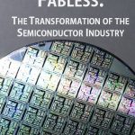
Copies of the 2019 updated version of “Fabless: The Transformation of the Semiconductor Industry” will be available compliments of Methodics. In addition to signing books I will be presenting my version of Semiconductors: Past, Present, and Future! In the Methodics theater. Stop by, say hi, and check the full theater schedule.

TSMC 2019 Open Innovation Platform® Theater (Booth #326) schedule is HERE.

Being the number one foundry does have its advantages and a massive ecosystem is one of them. It really is interesting to see what the fabless ecosystem is up to so you might want to take a look. Presentations start at 10:15 and end at 5:30pm with raffles in between. The presentations are 15 minutes, which is nice, and the presenters generally stay afterwards to answer questions so it is a great place to network.

Discover the Benefits of S2C’s FPGA Prototyping Solutions booth #952

In the last 15 years S2C Inc. has shipped more than 2,000 systems to over 400 customers including the top semiconductor companies around the world. Stop by and meet the S2C team and see the new AI on the Edge FPGA prototyping demo. See Compiled ONNX models in an FPGA prototype with an ARM Cortex A53 and Mali-GPU on a Xilinx Zynq™ Development Kit using an FPGA implementation of NVIDIA® Deep Learning Accelerator (NVDLA acceleration). You can also learn about Ultra-deep Trace Debugging, High-throughput Transaction-level Verification, and Multi-FPGA Design Partitioning.

If you see me walking around with a beautiful woman that is my wife of 35 years. This is her second Las Vegas DAC, the first being in 1985.  DAC has matured quite a bit since then but so have we so it will be a memorable experience just the same, absolutely.


Will a Lack of Ethics Doom Artificial Intelligence

Will a Lack of Ethics Doom Artificial Intelligence
by Matthew Rosenquist on 05-31-2019 at 5:00 am

If there was ever a time that ethics should be formally applied to technology, it is with the emergence of Artificial Intelligence. Yet most of the big AI companies struggle with what should seem a simple task: defining ethics for the use of their products. Without the underpinnings of a moral backbone, powerful tools often become a caustic capability for abuse. AI technology leaders must establish the guard-rails before chaos ensues.

As the great strategist Sun Tzu professed “Plan for what is difficult while it is easy, do what is great while it is small”. It is a tough challenge to find the right ethical balance when it comes to the complexity of Artificial Intelligence. Even more difficult is establishing a reasonable governance and sticking with it. However, as AI gains in power with vast amounts of data, it will impact almost every aspect of our lives, from healthcare, finance, employment, and politics. The benefits will solidify a deep entrenchment of AI systems in our digital ecosystem. Establishing parameters now is challenging, but it will be far more difficult to avoid catastrophe later if we populate the world with AI systems that can be misused.

AI for Everyone
AI/Ethics is crucial for the long-term security, privacy, and safety of those who are intertwined with the digital world. Organizations with forethought and true social responsibility will lead the way and separate themselves from companies who only use such initiatives as thin marketing ploys. But there are tradeoffs that these companies must weigh.

Autonomous systems are perfect for analyzing information from massive amounts of data that groups, classifies, builds profiles, and makes decisions with high degrees of accuracy, consistency, and scalability. Such abilities can be highly prized and profitable but is alarming from a privacy, security, and safety perspective. Should AI systems profile every person to determine the best way to influence them for any topic such as politics, religion, and purchasing preferences? Should they be empowered to make life-and-death decisions? What about AI systems which show preference or discriminate against social, racial, or economic groups? Even if it is accidental, occurring because a lack of design oversight, are these situations ethical?

Such systems have the power to change the world. And where there is power, there is money, greed, and competition. To purposely avoid certain use cases of AI systems comes with an opportunity cost of missed financial windfalls and prestige. Companies understand this trade-off and it is difficult to forego such lucrative prizes especially if their competitors may maneuver to seize them.

Early Moves
Currently, the efforts to establish ethics for the use of Artificial Intelligence is still in its infancy. There are academic, political, and business initiatives, but we are in the early stages of theory and practice. Whatever standards are created and implemented must be tested over time. The real validation will be around the perceived sacrifices of power and financial gain. Although consumers may feel all this is out of their control, in fact as a community, they have a tremendous amount of influence. Society can collectively support or shun organizations based upon their ethical choices, resulting in impacts to profits, influence, and power.

Acting Together and with Forethought
As consumers, we have a choice to support businesses that fall into 3 categories of maturity:

  • Irresponsible: Tech companies that have yet to publish ethical guidelines for their AI products and usages. With a lack of motivation, expertise, or simply only focus on self-interest, they have not taken steps to purposefully guide AI systems to remain benevolent. Instead, either by intent or ignorance, they will use AI for whatever pursuits benefit them without the burden of considering the greater consequences.
  • Striving:Organizations with a moral compass that have put forth the effort to establish AI Ethical policies but are struggling to implement the right balance. Time will tell what direction they go and their true level of commitment. Companies like Google, which recently disbanded their new AI ethics council, have worked hard to define a direction and governance but are finding difficulty in solidifying a structure that represents the optimal balance. Of note, Google does listen to its employees, partners, and the customers when it comes to inputs for decisions.
  • Leaders: Then there are those organizations, still few in number, who have fully embraced AI/Ethics with a greater level of social responsibility. They see both the opportunities and risks and are willing to forego some short term advantages for the betterment of all. They use AI with forethought and transparency to benefit their users, improve their services, and build trust by show their willingness to do what is right.As members of society, each of us should recognize and show economic support for the Artificial Intelligence ethics leaders and those who are continuing to effort attaining such a prestigious status. As citizens, our political support is crucial for proper regulations, enforcement, and legal interpretations that set a minimum standard for acceptable behavior and accountability. As consumers, voting with our purchasing preferences, we can make ethical AI leadership a competitive advantage.
    In the end, Artificial Intelligent systems will be analyzing our data and determining what opportunities and impacts will affect each of us. We have a responsibility to protect ourselves by supporting those organizations who are operating with purposeful ethical standards in alignment to what we deem acceptable.

    #artificial_intelligence #ethics #cybersecurity #AI


Siemens Shows SOC Simulation Solution for Self-Driving Vehicles

Siemens Shows SOC Simulation Solution for Self-Driving Vehicles
by Tom Simon on 05-30-2019 at 11:00 am

Ever since the early days of computing there has always been a large distinction between ‘regular’ computing and real time computing – where special care had to be made to deal with unordered and asynchronous events. Back then a system typically consisted of a handful of sensors and perhaps some electromechanical devices. The complexity back in those days pales in comparison to the challenges of building systems for automated driving in the present day. Each component of a self-driving car is part of an interdependent whole.

The goes literally from where the rubber meets the road to the high powered SOCs that make the whole system work. Due to the myriad interdependencies, it is not possible to simply build a prototype and test it to arrive at a correctly operating and optimized vehicle. It’s not enough that the AI hardware and software are working properly – sensors and actuators need to be accurate, and reliable. The physical properties of each need to be modeled so inputs can be properly interpreted, and controls are driven precisely. Piled on top of this complexity are the added requirements for safety. Systems in the vehicle need to be self-testing and failover has to occur seamlessly.

Siemens PAVE360 complete automotive design simulation solution

It is customary to make models of physical and electronic systems early in their design process to ensure that the designs are fully verified by the time they are manufactured. Scaling modeling and simulation up to the vehicle level is necessary for autonomous vehicles. The benefits of doing this extend beyond verification, allowing for iterative design improvement long before physical components are available. One such example is determining optimal sensor placement. Also, in the realm of AI, an accurate model of the vehicle can facilitate neural network training.

Closed loop simulation is so valuable in the automotive design space that Siemens has developed a simulation system that can model every element of a vehicle and mix real physical components with virtual ones to allow a wide range of system integration and simulation long before a real working vehicle is ever assembled. The system is called PAVE360.

One of the most interesting aspects to the PAVE360 is its ability to simulate custom SOCs using Mentor hardware emulation tools. In the maturing autonomous vehicle market, manufacturers are looking to improve performance by designing AI/ML SOCs tailored to their specific needs. This is a leading factor in creating product differentiation.

PAVE360 can model every aspect of a vehicle in operation. This not only includes simulating sensor input for real world operation, it also can cover 5G operation for V2V and V2I communications. This illustrates just how comprehensive the system is. Siemens believes that the availability of PAVE360 systems can help every member of the supply chain improve their products. It’s also not just for navigation. PAVE360 can be used for every system in a vehicle, including engine and drivetrain management, safety, infotainment, battery/fuel management, etc.

Siemens has developed a unique system for enabling early simulation of SOC designs in a comprehensive environment that covers every aspect of vehicle operation. Looking back at their acquisition of Mentor, there were many questions at the time about the value proposition. It seems now that building something like PAVE360 could only be done with their combined technology and resources. A PAVE360 installation is on display in the Center for Practical Autonomy Lab in Novi, Michigan. The details of this system are featured in the announcement by Siemens.