RVN! 26 Banner revised (800 x 100 px) (600 x 100 px)

Actel Goes Public – The IPO

Actel Goes Public – The IPO
by John East on 09-23-2019 at 6:00 am

In 1990 Xilinx notified us that they believed Actel was infringing a patent that had just been issued to them.  My immediate thoughts – the patent system is all screwed up!  Actel had been developing our product for five years. We had been shipping it for a year and a half.  During all that time, we were totally unaware that there was or ever would be such a patent —   there was no way to know that Xilinx had filed for a patent or what was in the filing.   Then,  when the patent finally issued  —- BAM!!  We’d been blindsided!!  The “normal” way to handle this situation is to take a license  — to agree to pay a royalty to the owner of the patent.  There was a problem with that.  Bernie Vonderschmitt (The CEO of Xilinx) didn’t want to give any licenses.  I can’t really say that I blame him for wanting to keep the FPGA market to himself.  It was hard to get mad at Bernie.  He was a classy guy.  Yet,  if it had gone to court and Xilinx had won,  they would have been completely within their legal rights to enjoin Actel from shipping our FPGAs.  That would have forced us to close our doors – to shut Actel down.  I spent the better part of three years trying to solve this potentially very, very serious problem.

In those days the rule of thumb was that a start-up could go public once they had achieved two consecutive profitable quarters.  We reached profitability in 1990 and were hot to go public.  We selected bankers  — Goldman Sachs was the bulge-bracket bank  —  and started preparation.  Then, Goldman’s lawyers started to get cold feet.  What if the patent battle couldn’t be settled?  If the worst case came to pass   — that is — we went public, took money from new shareholders, and then had to shut our doors because we had lost the patent suit —   the lawsuits would be everywhere. Eventually we had to put the IPO on hold.  (IPO = Initial Public Offering AKA “going public”.)

I’m not sure that we could have settled the Xilinx patent suit.  Bernie hadn’t shown any interest in doing so.  But then a good break came our way.  Khalid el Ayat found that the early Xilinx parts didn’t use what we called segmented routing but that their later family (the 4000 family) did.  One of our original patents had some claims dealing with segmented routing techniques (thanks Abbas El Gamal,  John Green and team).  That allowed us to file a countersuit against Xilinx.  Calmer minds prevailed.  We settled the suits peacefully.

Note:  Xilinx later sued Altera for infringing that same patent.  They weren’t able to settle and eventually went to trial.  My analysis was that Altera did infringe, but that the patent wasn’t valid over prior art.  The jury eventually ruled that the patent was indeed valid but that Altera didn’t infringe.  In my mind, wrong on both counts.   That’s the reason that you never want to go to a jury trial with a technical issue.  The jury won’t understand it and has an excellent chance of getting it wrong.  This case was very technical.  I doubt that the jury members understood 10% of what they were being told.

Once the Xilinx suit was settled,  our IPO efforts cranked up in full force.  Everything was looking good.  Then we hit another snag.  We had been selling 1.2 micron material, but we needed 1.0 micron product if we were to be cost competitive.  The process was ready to go,  or so we thought,  but the first production runs to come out had terrible yields.  If we couldn’t run the 1.0 process,  we couldn’t compete well cost-wise.  That would have to be disclosed in the IPO documents.  We had to put the IPO on hold for a second time.  Then, we cracked the code.  We figured out the problem and fixed it.  Thanks Steve Chiang!  Thanks Esmat. The IPO was back on.

IPOs are hard work.  Huge amounts of effort go into putting together the documents.  Everything that could end up mattering to a prospective shareholder must be disclosed and explained.  The explanations had to be right.  If the stock went down for any reason other than the market’s fickle nature,  you could expect a lawsuit.  The point of the suit would be that you hadn’t properly disclosed the risk of some aspect of the company and that if you had, the shareholders wouldn’t have bought the stock and hence wouldn’t have lost their money.  I spent many, many, many hours writing those documents. It took a long time and a lot of effort by a lot of people to get the documents ready!  Those documents are a big, big deal!

Once you have the documents done they must be approved by the Security Exchange Commission.  The SEC folks are tough.  They invariably find fault and demand improvements.  Once the SEC has given their approval,  you can start the “road show”.  The point of the road show is to meet with the people who are about to invest and teach them the basics of the company’s business. The road show is grueling.  You present the company pitch over and over and over again.  Breakfast presentations.  Morning one-on-ones.  Lunch presentations.  Afternoon one-on-ones.  Dinner presentations.  Then, you head to the airport, fly to a new city, and do it again.  One day we had a breakfast meeting in Minneapolis, a lunch meeting in Chicago,  a dinner meeting in Madison, and then flew to the east coast where a full day was set up for the following day.  When we landed, Dave Courtney (Our Goldman Sachs guy) had a message that our afternoon meeting the next day had been canceled.  That would mean that we had a couple of hours on our hands.  I suggested that we go see the Liberty Bell  — I had never seen it.  Dave thought that I was really stupid!  “John, the Liberty Bell is in Philadelphia.  We’re in Boston.”  Actually, I knew where the Liberty Bell was.  I just didn’t know where I was.  All the cities had become a blur by then.

A couple of days later in New York we got on a plane at Kennedy Airport and prepared to head home.  We were done!!!  It was a Friday afternoon.  We would celebrate over the weekend – then  – Monday morning when NASDAQ opened  — there would be a new listing:  ACTL.  Has a nice ring to it,  don’t you think?  ACTL!!!!!  Just before I boarded the plane, someone from Goldman brought me a fax that had arrived a few minutes earlier.  I took a sip from the glass of wine that I’d already treated myself to and opened the envelope.  It was a letter from a struggling start-up accusing us of infringing a patent of theirs.  I almost spit out the wine!!!  When I took a quick look at the patent, it wasn’t clear that it really applied to us.  But  — their timing was clearly calculated to get some quick cash from us.  The patent would constitute a new “risk factor” that should be disclosed to all potential investors.  To do that, though, would mean putting the IPO on hold for a third time  — redrafting and reprinting all of the documents, waiting a month or so for the new info to disseminate, going through SEC approval again and then doing the road show all over again.  Devilishly clever timing, don’t you think? But also, in my mind, completely without class.  We were supposed to “price” and open the market Monday morning.  The weekend when I planned to relax and celebrate was shot.  We sorted it out that weekend.  I don’t remember any details, but I’m sure it involved a tidy payment to the very clever offended party.  What I do remember is being really relieved that we had sorted it out.

Monday morning, August 3,1993 when they rang the opening bell*,  Actel stock was trading publicly right along with the likes of Apple and Intel!!  We opened at $9.50 per share.  During the day we ran up to $13.00. We were a public company.

Next week:  The Mars Rovers.

*Actually they don’t ring a bell at NASDAQ.  They just push a button.  It’s the NYSE that rings a bell.  I found that out in 2003 when I was invited to open the market as we celebrated our tenth anniversary of being a public company.  I gave a little speech,  waited a couple of minutes, and when they gave the sign, reached out and pushed a small black button.  Six years in college for that?!!

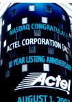
Pictured:  NASDAQ building at 42nd and Broadway in New York City on the celebration of our tenth year of being listed on NASDAQ.

See the entire John East series HERE.

# Bernie Vonderschmitt, Goldman Sachs, IPO, NASDAQ, Xilinx, Altera, Microchip


Criminals Luring in Bitcoin Sellers to Launder Money

Criminals Luring in Bitcoin Sellers to Launder Money
by Matthew Rosenquist on 09-22-2019 at 10:00 am

Cybercriminals are luring in bitcoin holders with the promise of easy money if they become a mule to convert stolen assets into clean currency. The reality is these volunteers will just join the ranks of other victims. But that is not stopping people from joining up to replace other mules who have paid the price.

Criminals are selling cash for pennies on the dollar to buyers willing to trade it for Bitcoin, according to the new Q3 2019 Black Market Report from Armor’s Threat Resistance Unit. A recent Cointelegraph article outlines how $800 in Bitcoin buys $10000 in cash on the Dark Web.

Digital cybercrime is a huge business, accounting for an estimated global cost of $3 trillion in 2015 and predicted to rise to $6 trillion by 2021 according to research from herjavecgroup.com.  A subset of that is monies stolen from victims which criminals want to launder so it cannot be traced back to them.

One of the most popular ways of laundering money is to use a 3rd party to transfer the money through their clean accounts.

For years, criminal outfits have been recruiting dim-witted volunteers to conduct such activities by giving them a percentage of the money they launder. This initially looks like a great opportunity for these volunteers but it is likely the worst decision of their lives.

Mules are a throw-away resource for organized criminals. They are the most exposed point to law enforcement and are often the ones caught. As the mules are purposely insulated from the criminals, they can’t negotiate a lesser sentence by informing who they work for. They are stuck with the burden of the full legal repercussions. The criminals simply recruit new mules to replace the old and leave a trail of discarded minions.

As for the mules who are caught, their future is pretty dark. First, they get arrested for a number of felonies. Supporting organized crime and transporting funds across borders are serious offenses. They should expect prison time. This gives them a lifelong criminal record of financial crime, which will then haunt them any time they seek employment at a company. What business would want to hire a thief? They may be put on travel watch lists, for fear of physically moving cash. The government will seize their assets and they will have to surrender or pay back all illicit profits to the government. Then, the IRS will come for them. Yes, they will still have to pay taxes on all the money they moved, not just their profits. This can be much more then they made being a mule. Those taxes also incur late fees.

Simply put, choosing to become a money mule for easy cash can ruin someone’s life. Doubtful the criminals tell all this in the job recruiting brochure.

It may be tempting, but don’t let yourself, family, or your colleagues be lured into this disaster by the promise of quick cash. Money laundering only helps the criminals and in turn, they will continue to victimize more people, including the mules.


Forget about 5G

Forget about 5G
by Roger C. Lanctot on 09-20-2019 at 10:00 am

There is a vast amount of hubbub in the automotive industry regarding the onset of 5G technology. Industry excitement is manifest in the 5G Automotive Association (5GAA) which is facilitating collaboration (among 120+ member) between the automotive industry and the wireless industry, possibly for the first time ever.

For years, cars and connectivity have gone together like fish and bicycles – in other words, not at all. General Motors’ OnStar automatic crash notification was a brilliant idea, but the arrival of the smartphone has almost completely erased any consumer enthusiasm for this application.

But cellular skeptics will be wise to arrest their tut-tutting about the future of connected cars because pre-5G LTE-based connectivity in the form of C-V2X is about to change everyone’s understanding of the value of connecting cars. More than 6,000 pedestrians were killed in traffic-related incidents in 2018 in the U.S., a 40% increase from 2008 and now representing 16% of all U.S. highway fatalities. That’s likely to get worse with the proliferation of micromobility. C-V2X is about to change that grim reality forever.

When Ford Motor Company announced its plans to adopt built-in C-V2X technology in all or most of its cars by 2022, the automotive industry shrugged. Ford had long trailed GM in its implementation of embedded connectivity – relying instead on connected smartphones with its clever SYNC solution created in partnership with Microsoft. Ford even found a way to enable automatic crash notifications from connected smartphones – i.e. 911 assist.

SYNC has since evolved, but so has Ford’s thinking about connectivity. The company’s singular embrace of C-V2X is likely to put the company in the vanguard of a movement to leverage vehicle-to-vehicle technology (enabled by C-V2X) and vehicle-to-pedestrian technology to reduce collisions between cars and between cars and pedestrians.

Enabling cars to “see” pedestrians is something of an industry Holy Grail. We’ve all seen the LiDAR images of pedestrians and even the camera-based and night-vision pedestrian detection systems. All of these modalities hint at the potential to use sensors to avoid collisions with pedestrians.

C-V2X, however, will enable so-equipped cars to detect the presence of pedestrians by “detecting” their C-V2X (or 5G enabled) smartphones. As C-V2X proliferates through mobile devices and, eventually, in cars, vehicles will increasingly be able to detect other vehicles and pedestrians.

This ability will initially manifest as driver alerts in dashboard-based systems such as the instrument cluster or infotainment system or even in head-up displays. Eventually, in-vehicle systems will be able to respond automatically, braking or taking other evasive action to avoid collisions.

Qualcomm will be holding an Automotive Showcase next Tuesday, Sept. 24, at the NextEnergy Center in Detroit, Mich., to demonstrate the capabilities inherent in C-V2X technology and explore new life-saving applications. There is no doubt that 5G, when it arrives in the U.S., will have its own transformative impact on vehicle technology development and deployment, but C-V2X will arrive even sooner in cars and in mobile devices.

Gil-Scott Heron was wrong. This revolution WILL be televised…in your dashboard.

Register for the Qualcomm Automotive Showcase here: https://tinyurl.com/yxawjuse


Chapter Eleven – International Semiconductor Competition

Chapter Eleven – International Semiconductor Competition
by Wally Rhines on 09-20-2019 at 6:00 am

Semiconductor industry evolution was largely a U.S. phenomenon.  While there were important contributions made by persons all over the world, the basic technology grew from the invention of the transistor at Bell Labs which was licensed broadly in the U.S.  That created a level playing field for all who wanted to become producers.  The industry then evolved in a free market environment in the U.S. largely without regulation or patent disputes. By 1965, three companies, TI, Motorola and Fairchild, had a combined market share greater than two thirds of worldwide sales of semiconductors (Figure 7, Chapter Five). Barriers to the internationalization of the industry emerged through import tariffs in Europe and restrictions on setting up subsidiaries in Japan but even these limitations gradually disappeared.

After 1965, the semiconductor industry began a near continuous deconsolidation as new companies entered the market.  The market share of the largest competitor remained about the same for the next fifty-five years at 12 to 15% (Figures 7 and 8 in Chapter Five). Top ten semiconductor companies during the 1950s and 1960s did not include any non-U.S. companies (Figure 10, Chapter Five).

Japan Becomes a Significant Competitor
In the late 1970s and early 1980s, the industry became international with the entry of NEC, Toshiba, Hitachi and Matsushita into the list of the top 10 largest semiconductor companies. Philips, a European semiconductor company, also entered the top ten for the first time. The Japanese phenomenon was driven largely by the superior manufacturing process control applied to dynamic RAMs, or DRAMs.  This was the first wave of “trade wars”.  The Japanese Ministry of Industry and Trade, MITI, coordinated actions among Japanese companies that contributed to a cooling of tensions between SIA (U.S. Semiconductor Industry Association) and EIAJ (Electronics Industry Association of Japan).  Japanese companies were assigned quotas for purchases of semiconductors from U.S. companies, relieving some of the pressure.  The real end to the issue was predictable but not so obvious to many of us.  At a dinner I had with Saturo Ito, CEO of Hitachi Semiconductor, in the late 1980s, he explained to me that the U.S. shouldn’t worry about Japan taking over most of the manufacturing of semiconductors in the world, as I had feared.  Ito told me, “Japanese are optimizers, not inventors.  When standards are stable, Japan will do well.  When standards are evolving, not so well.”  He was right.  As the personal computer and cell phone industries grew, the U.S. recaptured substantial innovation momentum.

Enter Korea
Less predictable than the Japanese success in DRAM manufacturing was the entry of Korea.  When Samsung announced its intent to design and produce the 64K DRAM and sent their managers on a 64-mile hike as a symbolic start, we didn’t pay much attention.  How could they catch up in an industry that was so mature?

Their success came from the determination of Koreans when they decide upon a specific goal.  The path was not easy.  As late as 2008, the combined market share of the three largest DRAM producers in the world, Samsung, SK Hynix and Micron, was only modestly greater than 50% of the entire worldwide market.  Today, their combined market share is greater than 95% (Figure 6 of Chapter Five).

Taiwan
As with Japan, Korea and China, Asian governments understood very early the importance of domestic semiconductor capability.  Evolution of worldwide leadership in the silicon foundry business by Taiwan is truly remarkable. The Taiwanese semiconductor industry grew from a team of Taiwanese engineers who went to work for RCA in the late 1970s.  These individuals were very talented.  They started many semiconductor companies when they returned to Taiwan.  When the Taiwanese government formed ITRI and ERSO to promote advanced development in Taiwan, the country was fortunate to have Morris Chang, former head of TI’s semiconductor business, available to move to Taiwan to head up these two entities.  When TSMC and UMC were formed, Morris filled the role of Chairman of both.  Securing funding from Philips, he was able to take advantage of an unlikely transition of the semiconductor industry.  Those of us in the industry at the time wondered how a company whose business consisted only of wafer fabrication could ever survive.  Those of us working for integrated device manufacturers like TI viewed wafer fabs as our biggest problem.  Whenever a recession came along, the fabs became under-loaded and were astoundingly unprofitable.  The depreciation cost continued but the revenue did not.  If someone else was willing to take over the wafer fabs, then the semiconductor business volatility would be reduced making it a more attractive, stable industry. The U.S. had already experienced the pain of wafer fab ownership when Japanese competitors in the 1985 recession kept running wafers at a loss, partly because they couldn’t lay off their people.  In the U.S. we shut down some of our wafer fabs to stop the financial bleeding.  Step by step we created an opportunity for Japan to gain market share when the recovery inevitably came. Now TSMC and UMC in Taiwan were taking over the one aspect of the industry that caused us the greatest pain.

TSMC recognized the value of being a dedicated foundry with no products of its own to compete with its customers, unlike its competitors such as UMC, Seiko Epson, NEC and more.  By becoming a pure play foundry and popularizing its design rules, TSMC gained momentum that was hard to match.  Today, only Samsung comes close to providing real competition at the leading edge of semiconductor technology.

This leaves the U.S. in the interesting position that, other than Intel plus some limited capacity in Texas and New York, there is no significant domestic manufacturing capability at the advanced nodes of semiconductor technology. Anything that disrupts free trade between Taiwan and the U.S. could severely disrupt much of the U.S. manufacturing and defense industries.

China
Despite China’s rise as the world’s largest assembler of consumer electronic equipment, the Chinese semiconductor industry has evolved slowly. The largest Chinese semiconductor foundry, SMIC, is still two technology nodes behind TSMC in manufacturing capability as of 2019.

The Chinese government is dedicated to changing this situation.  Figure 1 shows the investment that is being made.

Figure 1.  Chinese government stimulus for semiconductor investment has been matched by a much greater investment by private equity companies

These numbers dwarf anything that the U.S. government is likely to do.  The entire annual revenue of the worldwide semiconductor industry is less than $500 billion.  The Chinese government is investing more than $20 billion per year.  They are doing it in an insightful way.  The money is invested as a share of private equity companies who are motivated to invest in semiconductor companies that can make an attractive return on the investment.  Many of the startup companies have an optimistic outlook because the Chinese population of over one billion people can drive its own standards for communications and computing.

How well have they done with the investment?  Figure 2 shows a comparison of the size of the semiconductor companies that have benefited from the investment.

Figure 2.  Growth of Chinese fabless semiconductor companies

Average employment of the semiconductor companies in China has grown between 2006 and 2015.  The number of companies with more than five hundred employees in 2006 was less than one half of one percent. In 2015, it was 6.1%.  The number of Chinese fabless semiconductor companies that had between 100 and 500 employees in 2006 was 9.8%.  In 2015, it was 43.3%.  This growth provides a challenge for semiconductor competitors in the rest of the world including the U.S. where governments can’t afford to provide the kind of subsidies that are available in China.  Even so, the problem was manageable with innovative U.S. companies operating in a semi-free market environment for creating new technologies.  The U.S., however, created a “Sputnik moment” for China that may have changed the outlook.

Historical Perspective of Export Controls
In 1982, I joined the Technical Advisory Committee of the Department of Commerce that was set up to advise the Department regarding the granting of validated licenses for export of semiconductors and semiconductor manufacturing equipment.  Soon I became Chairman of the committee.  In the 1970s, U.S. companies like Applied Materials, Lam Research, Novellus, Varian and many more dominated the worldwide semiconductor manufacturing equipment business.  Japanese companies like TEL were growing but their base of customers was largely in Japan.  The Export Administration Act of 1979 was one of the contributing factors that changed that competitive situation. Concern about the military implications of semiconductor capability led to a set of restrictions on semiconductor related exports from the U.S. and its allies to controlled destinations that were enemies of the free world.

Allies like Japan were much more efficient at administration of bureaucratic export control rules.  Validated licenses for customers of Japanese manufacturers could reliably be obtained in three days plus or minus a day or two.  For the U.S., the time and the variability were much greater.  Companies in places like Taiwan rightly concluded that the U.S. could not be trusted as a supplier because spare parts and user manuals also required separate validated licenses.  Market share of U.S. companies in the semiconductor manufacturing equipment industry fell from more than 4X Japan’s market share in 1980 to about equal shares for Japan and the U.S. in 1990. In a sense, the U.S. moved toward a role as the “vendor of last resort” for semiconductor manufacturing equipment sold to controlled destinations and probably even to some destinations that were COCOM allies.

China’s Sputnik Moment
ZTE clearly violated internationally accepted export restrictions on Iran.  The U.S. reaction was not totally unexpected.  What surprised the world was the swift action taken to shut down the free market purchase of semiconductor components.  The degree of dependence that ZTE had developed upon U.S. semiconductor suppliers made this a life or death issue for the company.  President Trump ultimately waived the export restrictions. Although the embargo was lifted, the impact of the threat was now apparent to China.  Dependence upon U.S. suppliers of semiconductors was no longer a viable strategy.

As the Chinese government continued its move toward dictatorship, rules were imposed upon foreign companies for the opportunity to establish operations in China. Google was prevented from operating in China, as were others. These restrictions became increasingly egregious (such as the threat that U.S. software companies might have to turn over their source code to the Chinese government if they wished to operate in China). As frictions developed in the trade negotiations between the U.S. and China, a U.S. decision was made to embargo exports to Huawei by placing Huawei on the “entity list”. This created an even more untenable situation for China, the worldwide leader in wireless communication technology.

China did the expected.  They focused upon developing non-U.S. capabilities for all their components.  Since China buys more than 50% of all semiconductor components in the world, this is a big problem for the U.S. semiconductor industry.  It is probably not reversible.

Another question is whether other countries will follow suit out of fear that political disagreements with the U.S. could result in an embargo of semiconductor components from U.S. suppliers. As with the Export Administration Act, events in China will lead to a reduction in market share of U.S. based semiconductor suppliers and a loss of their lead in many new technologies.

How long will it take for China to eliminate its dependence upon U.S. semiconductor suppliers?  Probably many years, especially for FPGAs and RF components, and it may never be achieved.  China’s demand is so large that non-U.S. suppliers will probably find a way, given enough time, to displace U.S. suppliers but it’s hard for any country to become totally self-sufficient.  In addition, China’s move toward a closed, controlled society will restrict innovation. That will work to the advantage of the U.S.

While China’s direction is not likely to change, we still have the possibility of convincing the rest of the world that the U.S. can be treated as a reliable supplier.  Hopefully, there will be policies articulated by  the U.S. that convey that confidence and restore the U.S. position as a leader in free trade.


Is Samsung having problems with 7NM? Do long lines at TSMC prove that?

Is Samsung having problems with 7NM? Do long lines at TSMC prove that?
by Robert Maire on 09-19-2019 at 2:00 pm

Reports of increasing TSMC 7NM lead times
There have been a number of increasing media reports about lengthening leads times for TSMC 7NM process. From what we have been able to determine its not due to TSMC having a yield bust or other production issues, it is simply one of stronger than expected demand.

There have been reports of up to 6 month lead time quotes which is untenable for companies that need to keep releasing newer, faster, better versions of products to stay ahead of the pack or at least keep up with the pack.

This begs the question as to whats happening in the leading edge foundry market? Normally there is some sort of balance between TSMC and Samsung with each taking a portion of leading edge business and customers, such as Qualcomm, like it that way so they are not dependent upon one supplier who would otherwise have them over a barrel.

Or are they??

Samsung 7NM yield problems?
It sounds as if Samsung is having yield issues at 7NM. This may be a repeat of Samsung’s 10NM which was prematurely pre-announced and then fell flat. If foundry customers can’t get yield from Samsung then TSMC is the only 7NM game in town and the lines will be out the door (like they apparently are…).

With GloFo dead and everyone else years behind, TSMC may be opening up an unstoppable lead.

Is EUV the culprit?
Samsung has been very aggressive in pushing EUV , in their foundry operations, and suggesting they had the lead in EUV and their designs would be far superior.

Samsung was obviously trying to tweak Apple into re-considering using their “frenemy” Samsung as a foundry ever since Apple dropped them.  Apple has had a high interest in EUV due to potential power savings and other benefits.

It seems as if Samsung may have bit off more than they could chew and the aggressive use of EUV for more layers may be the cause of the yield problems.  They were basically pushing something that was not yet ready for prime time.

Its going to be both hard and embarrassing to reverse course and reduce EUV use now to get yields back up….not pretty.

Maybe Intel is smarter than we think for go slow on EUV
Intel has been slower than both TSMC & Samsung in the adoption of EUV.  Perhaps its because of being gun shy after the 10NM debacle or perhaps they understood the challenges better.

It may turn out that go slow on EUV may have reduced the risk of another yield black eye, which Samsung may be dealing with now.

TSMC is the only game in foundry town
TSMC has been all but unstoppable. They have kept up the Moore’s law cadence without a hiccup and recently said that Moore’s law has a long life ahead of it. If customers want bleeding edge chip performance there is clearly one game in town.

TSMC should be able to make bank on this advantage in the market. Now just with 7NM but future generations as well as more customers will sign up for 6NM, 5NM and beyond.

Customers of Samsung will have to pay up big time when they go to TSMC to get devices foundered. This just accelerates the move to TSMC that was already occurring but turns it more into a stampede

Collateral Damage & Benefit

ASML
Obviously if EUV is finally revealed to be the issue it would be a large negative for ASML from a PR perspective.  From an actual P&L perspective I think there would be minimal damage as ASML is sold out on EUV any way.

EUV is absolutely inevitable but it was clearly very difficult and long to get machines built and just as hard to get the process to work. ASML can still point to TSMC’s success and Intel’s future success and probably shift the blame to Samsung.

Its unclear where the yield issues may specifically be and we may never know for sure….just like Intel at 10NM

Apple is safe
Apple has been TSMC’s BFF for a number of nodes now and they are fully signed on with TSMC and TSMC will bend over backwards to get Apple al the chips it needs, so no problem here. They have a permanent pass at the velvet rope.

AMD also in good shape
AMD threw all its eggs into TSMC’s basket, and while not nearly as big as Apple or others, they are clearly a friend of TSMC. They have also signed on for wafer production so they already have secured their place in line.

The only issue here is that if AMD has huge share gains against Intel they may be supply limited as they likely signed up for a specific amount of production which was probably a conservative number.

Qualcomm has a problem
Qualcomm is or was the most significant customer of Samsung, trying to split the business with TSMC to diversify supply and play them off against one another. Now they have to go back to TSMC and get on the end of the 7NM line and probably pay a premium to boot. Not a good place to be right now especially with the hypercritical roll out of 5G coming up right now.

Qualcomm has absolutely no choice but to pay whatever TSMC demands and sign up for whatever TSMC wants.  The timing couldn’t be worse for them. The Samsung yield issue could cause a major problem for Qualcomm’s on time roll out of 5G. I would imagine that Qualcomm might think twice about risking future production with Samsung.

While investors are all excited about 5G, a delay could be a big blow which could cause a drop in the stock especially if they had to announce it.  We would consider being light or short the stock if this pans out.

Broadcom is happy
As both a customer and friend of TSMC , Broadcom has no problems and obviously could benefit at Qualcomm’s problems if Qualcomm can’t get new 7NM parts in a timely manner.  Broadcom does not have a significant Samsung exposure so little downside.

Intel could use FUD factor against AMD
Although Intel gets no direct impact either way they could try to put the FUD (fear, uncertainty & doubt) factor into customers minds who can choose between AMD and Intel by questioning AMD’s ability to deliver based on growing TSMC lead times.  We don’t see this as a real issue but it could cause problems.

Samsung
Obviously Samsung is already suffering under poor memory pricing with the prospects of a very slow memory recovery.  The foundry side of the business did not account for a lot of external revenue, especially when compared to memory but none the less it would be a further blow to Samsung’s revenue coming at a very bad time given that semiconductor sales is the vast majority of Samsung’s profits. This is of course not to mention that Samsung makes its own processors for its phones whose supply could also be at risk.

This is on top of the risk of supply of semiconductor materials from Japan that are threatened to be cut off. A yield problem at 7NM is the last thing Samsung needs right now.

This of course adds to the probability that Samsung’s spending will remain low as they now have even less semiconductor revenue to pour back into their fabs.

Not pretty at all….maybe a “short”

KLA
Given that KLA specializes in yield management and increasing yield and finding problems it could benefit from any added spending to find and fix the problems as well as prevent future problems.

Nothing helps the sale of process monitoring equipment like a good yield bust…..


Speeding Up Physical Failure Analysis (PFA)

Speeding Up Physical Failure Analysis (PFA)
by Daniel Payne on 09-19-2019 at 10:00 am

Mentor - design defect

The cost of an IC depends on many factors like: NRE, masks, fabrication, testing, packaging. Product engineers are tasked with testing each part and understanding what exactly is limiting the yields. Every company has a methodology for Physical Failure Analysis (PFA), and the challenge is to make this process as quick as possible, because time is money especially when using testers that can cost millions of dollars.

Volume scan diagnostics is a popular method for creating defect paretos and plotting yield, and the larger the sampling size the better the accuracy. There are many challenges for product engineers these days:

  • Larger design sizes slow down testing
  • New process nodes have new failure mechanisms
  • Cell-aware diagnosis takes more time
  • Compute resources are growing

Let’s take a closer look at what happens during volume scan diagnosis; a design netlist is read into a simulator along with scan patterns and the log from a failing chip. To handle multiple fail logs quickly the diagnosis is simulated in parallel across a grid of computers.

With large designs there can be practical computational limits to scan diagnosis, so let’s assume that your design takes 100GB of RAM and requires an hour for each diagnosis. If your compute grid has 11 machines as shown below:

Only Machine 1 has enough RAM to fit the design and with 2 parallel jobs it will diagnose only 48 results per day. Machines 2-11 don’t have enough RAM to fit the design, so they remain idle.

The actual diagnosis throughput can be described as an equation that depends on how much diagnosis memory and diagnostic time is required.

To shorten the diagnosis throughput requires that we somehow reduce the memory and time requirements, and it turns out that a technique called Dynamic Partitioning as used in the Tessent Diagnosis tool from Mentor does this.

In the following figure we see a design fragment with three scan chains, and a defect is found in the top logic cloud which then causes two scan bits to fail in the second scan chain shown as red logic values. Using dynamic partitioning only this design fragment needs to be simulated by Tessent Diagnosis, thus requiring much less RAM than a full netlist.

Here’s the smaller partition that needs to be simulated:

With Tessent Diagnosis Server all of the dynamic partitioning is automated and it works with your compute grid setup, like LSF, so that run times are minimized.

You can even choose the number of partitioners and analyzers to be used on your grid, where the partitioners automatically create dynamic partitions for diagnosis and analyzers do the diagnosis on the smaller partitions.

Let’s go back to the first test case and this time apply dynamic partitioning:

With dynamic partitioning the diagnosis throughput jumps from 48 results/day up to 528 results/day because all 11 machines can be utilized in parallel. Two test cases from actual designs show throughput improvements between 11X and 16X faster by using dynamic partitioning:

When using dynamic partitioning there’s no change in the quality of the scan diagnosis result, you just get back results much quicker from your compute grid using less RAM.

Summary

Divide and conquer is a proven approach to simplifying EDA problems and for product engineers doing PFA there’s some welcome relief in improving throughput based on dynamic partitioning technology. The old adage, “Work smarter, not harder”, applies again in this case because you can now use your compute grid more efficiently to shorten volume scan diagnosis.

Read the complete 6 page White Paper online, after a short registration process.

Related Blogs


WEBINAR: AI-Powered Automated Timing Arc Prediction for AMS IP’s

WEBINAR: AI-Powered Automated Timing Arc Prediction for AMS IP’s
by Daniel Nenni on 09-19-2019 at 6:00 am

A directed approach to reduce Risk and improve Quality

Safety and reliability are critical for most applications of integrated circuits (ICs) today. Even more so when they serve markets like ADAS, autonomous driving, healthcare and aeronautics where they are paramount. Safety and reliability transcend all levels of an integrated circuit and the quality of timing definition at every level plays a critical role in ensuring them. Every integrated circuit, small or big, uses from tens of IP’s to hundreds of them. Proper timing behavior of every component is key to the overall safety and reliability of the IC and the system the IC goes into. Creating a comprehensive set of timing arcs for the IPs is an essential component of its quality metric and ensures better safety and reliability in the end applications of the IP. It also plays a key role in the reduction of a variety of risk factors for the IP and the IC it goes into.

Timing arc generation for digital IPs is well understood and is automated. The same is not true for the analog and AMS IP’s. Timing arc generation for analog and AMS IP’s is manual. In addition, IPs get integrated into many applications beyond what an IP designer designed his/her IP for. It relies on the designer’s expertise to not miss an arc. How can you trust the SoCs that make use of such analog and AMS IP’s created using error prone methods for mission-critical applications like autonomous driving, aeronautics, healthcare? An AI-powered methodology that allows the generation of a comprehensive set of timing arcs analog/AMS IP’s – high quality and low risk – is essential for their use on mission-critical applications.

Integration of analog or AMS IP into a SoC is challenging and the larger the IP, the greater is the challenge. With analog designs being sensitive to layout, proximity and matching, the impact on timing is direct and typically ranges from delayed tape-out to silicon failure, and multiple silicon iterations.

Thanks to recent advances in artificial intelligence (AI) and machine learning (ML), automation of the timing arc generation for analog and AMS IP’s is becoming a reality. Empyrean Software, working with some key customers has taken the lead to develop the automation of timing arc creation for analog and AMS IP’s. A joint paper, Machine Learning based Timing Arc Prediction for AMS Design, with a customer (NVIDIA) was presented at the “Designer Track” of the most recent Design Automation Conference (DAC 2019) in Las Vegas, Nevada.

A webinar titled, “Reduce Risk and Improve Quality of AMS IP’s using AI-Powered Automated Timing Arc Prediction,” will focus on the new AI-powered automated timing arc prediction and validation capability, the first commercial capability of its kind for IPs. It will talk about the motivation., technology and a methodology for using AI-powered automated timing arc prediction. The 30-minute webinar is scheduled for September 24th at 10:00 am (PST) and you can register to attend and get access to the presentation.

About Empyrean Software
Empyrean Software provides electronic design automation (EDA) software, design IPs and design services, including analog and mixed-signal IC design solutions, SoC design optimization solutions, and Flat Panel Design (FPD) solutions and customized consulting services.

Empyrean Software is the largest EDA software provider in China, and its research and development team has more than 30 years of experience in technology and product development. Our company has comprehensive cooperation with many corporations, universities and research laboratories.

Empyrean’s core values are dedication, collaboration, innovation, and professionalism. Our company is committed to working with customers and partners through win-win collaboration to achieve our common goals.


The Korea/Japan trade war benefits US more than US/China hurts US

The Korea/Japan trade war benefits US more than US/China hurts US
by Robert Maire on 09-18-2019 at 10:00 am

Investors underestimate Japan/Korea trade war, US chip equip companies get collateral benefit, Long term share shifts in China & Korea, Creates near term upside for US companies, Memory Chip Price “Mirage”.
The lesser known trade war
While the market and the news has been pre-occupied with the ongoing soap opera of the US-China trade war and its star power performers, Trump & Xi, there has been an escalating war going on between Japan and Korea that may have as much or more impact for some companies as compared to the US-China trade war.
We too, have been guilty of talking about China for several years now as they are clearing vying with the US for technology dominance and it has the importance of that struggle on a global stage.
While the trade war between Korea and Japan may not be for global dominance as neither country is on par with the US or China, it is still a blood sport with very important consequences for global markets, company profitability and national honor.
Long memories- back to WW2
The issues between Japan and Korea go back to World War 2 and prior as Japan ruled over Korea from 1910 to 1945. The issue of “comfort women” continues as the main symbol of the animosity.
This came to a head when the Korean supreme court recently allowed Koreans to sue Japan over damages from the “forced labor” in WW2.
Japan retaliates where it hurts- in semiconductors
Japan’s response was to restrict exports to Korea of key resist and etching gases that are critical to manufacturing both semiconductor and flat panel displays.  Korea is almost 100% reliant on Japan for this and semiconductors and flat panels and associated products are clearly the lifeblood of Korea’s economy.
Take a look at Samsung’s quarterly reports and you understand how bad things would be without chips.
Thus Japan’s restriction is in essence a “death threat” to the entire Korean economy.
The reaction in Korea has been swift as expected
The reaction in Korea is about the same as China’s reaction to the death threats against Huawei by the US and the actual death of the Jinhua memory fab at the hands of the US….Korea has gone ballistic….
Both the Korean government as well as Korean businesses are now hell bent on fixing the dependency on Japan but more importantly going many steps further and cutting off as much business from Japan as is possible, as quickly as possible.
Korea has choices that China doesn’t

Korea has the ability to find other vendors to replace Japanese companies especially in the semiconductor business.

Tokyo Electron which is the second largest semiconductor equipment maker in the world after Applied Materials stands to lose a whole lot of business as the Koreans can choose from Lam, Applied, ASM International and a number of domestic suppliers such as Semes. They could even go to China to the recent IPO, AMEC.
China’s Jinhua didn’t have this many alternatives to stay alive. China still wants to do business with the US and the US with China but in Korea, its blood & personal pride against Japan.  The trade war between the US and China is exclusively about money without a lot of other emotion mixed in.
 
US semi equipment gets collateral benefit
Much of the deposition and etch equipment used in semiconductor production, especially for non critical applications, is a bit of a commodity with pricing being a significant selection factor.   TEL has picked up a lot of share in recent times and the Japanese have a long history of cutting prices to the bone just to retain customers and employment. Many times US companies bow out of the “race to the bottom” against Japanese companies.
However we are now in a situation where US and other non-Japanese equipment companies may not have to have the lowest price to get the business and perhaps will win business just by being close enough that Korean customers can avoid the distaste of having to buy a Japanese product.
 
Near and long term benefit
We think the impact of avoiding Japanese products has already been started as we think some companies we know have already won business they otherwise wouldn’t have gotten.
Korea has also made it clear that they are re-evaluating their long term supply partners so the anti-Japan sentiment of today will likely be institutionalized for the future.
Although we think there was both long and short term damage to US and China relations due to the trade war, we think there will be less long term damage once the US and China work out a trade agreement whereas animosity will remain between Japan and Korea as it has festered just below the surface for many, many years.
 
US companies could see pick up without memory recovery
While we still need memory to recover to get a true recovery, we think there could be enough share shift between US and Japanese companies in Korea to see a meaningful uptick in business without memory capex coming back.   Korea has also been the biggest buyer of Japanese equipment and if much of that buying goes elsewhere (mainly to the US) it will look a lot like a broad based spending recovery.
We think the potential gains in Korea could out weigh potential losses in China so it would be a net win for US companies. While China is not far from being a bigger spender than Korea in semiconductor equipment we think the US will gain more in Korea than it can possibly lose in China in the long run.
The “Memory Mirage”
We would caution investors not to read too much into memory pricing given the backlog of idled capacity in all the fabs.
More importantly, we think there has been a bit of an “artificial” inflation of memory pricing due to concerns about Korean production being curtailed due to Japan cutting off key materials.
In short we think memory users have been “stocking up” to offset any supply disruption in memory and as such the recent stabilization in pricing/demand for memory may have a lot more to do with “stockpiling” than a true recovery or stabilization.
If Japan and Korea work out their differences, at least in critical materials, the stockpiled memory and artificial buying unwinding could cause another blip or return to a weaker environment.
The stocks
We think that most semi equipment stocks in the US should see benefit with Lam being perhaps one of the biggest winners as it had also been the biggest loser on the way down. KLA in the US and ASML in Europe are perhaps the least impacted as there is minimal Japanese competition.
Applied Materials will also clearly benefit as it does not yet own Kokusai and is not seen as a Japanese company in Korea. Perhaps KKR is the lucky one here unloading a largely commodity company just before a trade war may cut off one of Kokusai’s largest markets.  It certainly makes the Kokusai deal look even more costly than it already looked….maybe Applied can back out or re-negotiate.
We think that we may already hear of positive benefit when companies report their current, September quarter. Although we are still far away from a memory recovery a pick up from share shift in Korea could help define a bottom to the current cycle which would make investors as well as companies happy.
We would be net buyers of the stocks.  For those more adventurous investors we think strategies such as long Lam, short Tokyo Electron might be an interesting pair trade.

Glasses and Open Architecture for Computer Vision

Glasses and Open Architecture for Computer Vision
by Bernard Murphy on 09-18-2019 at 6:00 am

Fisheye view

You know that AI can now look at an image and detect significant objects like a pedestrian or a nearby car. But had you thought about a need for corrective lenses or other vision aids? Does AI vision decay over time, like ours, so that it needs increasing help to read prescription labels and identify road signs at a distance?

In fact no. But AI-assisted vision, generally called Computer Vision (CV), trains on undistorted, stable images in decent lighting. Let’s pick those assumptions apart, one at a time. To get a nice flat-field image in front of (or behind) your car you could use multiple cameras with relatively narrow-angle lenses, studded along the fender. That would be very expensive and power-hungry. Or you could use a single camera with a very wide-angle lens (see above). Much better cost-wise but there’s a bit of a problem with distortion.

This is correctable through a process known as dewarping, a geometric transformation of the image and a process which is already well understood. Image stabilization is another familiar technique, correcting for the jitters in your hand-held camera or a GoPro on your helmet as you’re biking down a rocky slope.

There are fixes for these problems today, but these generally add devices or multi-purpose IPs, cost and more power consumption. That can be a real problem in consumer devices because we don’t like more expensive products and we don’t want our battery to run down faster. It’s also a problem for the sensors in your car. More AI processing is moving to the sensors to reduce bandwidth load on the car network, allowing sensors to send objects rather than raw images to the central processor.

CEVA and Immervision, a developer/licensor of wide-angle lenses and image processing technologies, announced a strategic partnership just last month. For a significant investment in Immervision, CEVA gained exclusive licensing rights to their portfolio of patented wide-angle image processing technology and software. CEVA has also licensed technology from as a part of this deal for better image quality and video stabilization.

(Incidentally, as a part of the same deal, CEVA also licensed Data-in-Picture technology which integrates within each video frame fused sensory data, such as that offered by Hillcrest Labs, also recently acquired by CEVA. CEVA seems to be putting together a very interesting business proposition in CV – watch this space.)

If you need a low cost, low power solution in a consumer device or a car or in many other applications, it makes sense to integrate these capabilities directly into your CV solution. That’s what CEVA have done with their just-announced NeuPro-S IP which bundles in the vision processing software. So you can have a single fisheye backup camera at low cost, low power and probably higher reliability than multi-chip solutions.

There are a lot of other interesting features in the NeuPro-S including integrated SLAM and safety-compliance for which I’ll refer you to the website link below. But there is one feature I thought worthy of special mention in this short blog. Multiple AI accelerators from multiple sources are starting to be integrated together in single-chip implementations. This raises an interesting question – how do you download training to all these accelerators? Standalone solutions per accelerator don’t look like a great solution.

CEVA have invested heavily in their CDNN deep-learning compiler mapping with optimization from the most common training frameworks/networks to inference networks on edge devices. The optimizations include advanced quantization algorithms (mapping from floating-point to fixed-point), data flow management and optimized CNN and RNN libraries to run on the edge.

Now CEVA have opened up the CDNN interface, through a feature they call CDNN-Invite, to support not only NeuPro and CEVA-X and XM platforms but also proprietary platforms, making support for heterogenous AI a reality on edge device while still keeping the simplicity of a unified compiler interface. I like that – open interfaces are almost always a plus.

You can learn more about the NeuPro-S HERE. (need link)


Learn About Implementing SmartNICs, an Achronix White Paper

Learn About Implementing SmartNICs, an Achronix White Paper
by Randy Smith on 09-17-2019 at 10:00 am

We have all seen the announcements to provide ever-increasing network capabilities within the data centers.  Enabling these advances are improvements in connectivity including SerDes, PAM4, optical solutions, and many others. It seems 40G is old news now, and the current push is for 400G – things are changing very quickly. These advancements focus on high-speed transmission of data within the data center. What has not been talked about as much is the extra burden that can be added to the processors themselves to manage all this traffic. What would be the point of connecting all of these blazingly fast processors if all their efforts only go towards talking to each other? Into the breach stepped “SmartNICs,” also known as intelligent server adapters (ISAs). These devices can offload a lot of these network-management tasks from the host CPUs.  A SmartNIC allows you to use those CPUs for meaningful work, not just networking and housekeeping.

SmartNICs have been in the discussion for several years now, though the name has been used more like a marketing term without a clear definition. One short definition is that a SmartNIC:

  1. Implement complex server-based functions requiring compute, networking and storage
  2. Support an adaptable data plane with minimal limitations on functions available;
  3. Work seamlessly with existing open-source ecosystems.
Figure 1: Traditional NIC vs. SmartNIC

As I said, this is the “short definition.” This topic is quite intricate. Fortunately, Achronix has now released a white paper titled, How to Design SmartNICs Using FPGAs to Increase Server Compute Capacity. The paper initially discusses the three forms of SmartNICs in use today – Multicore SmartNICs, based on ASICs containing multiple CPU cores; FPGA-based SmartNICs; and FPGA-augmented SmartNICs, which combine hardware-programmable FPGAs with ASIC network controllers.

As you will have noticed from the white paper title, Achronix uses FPGAs in its SmartNIC solution.  The reasons for this are the limitations inherent in a multicore SmartNIC design. Multicore SmartNIC designs usually include an ASIC that incorporates many software-programmable microprocessor cores. The cores used may vary, but these solutions are still expected to be limited for two reasons: (a) They are based on software-programmable processors which are slower when used for network processing due to a lack of processor parallelism; and (b) The fixed-function hardware engines in these multicore ASICs lack the data-plane programmability and flexibility that is increasingly required for SmartNIC offloading. Using multiple cores cannot achieve the parallelism gained from using numerous custom pipelines in an FPGA.

Figure 2: Adding a Separate QoS Engine to Manage SLAs

There are many combinations and layers of features available when building a SmartNIC with an FPGA. The Achronix white paper goes into these variants in detail. I found it particularly good at describing the architectural modifications to achieve specific features. The white paper focuses on the concept, architecture and implementation of a SmartNIC using FPGAs and is something that anyone with interest in this area should pick up. You will find a long list of white papers, including this one, provided by Achronix on the documentation section of their website. This white paper requires minimal registration information to access.

I felt I learned a lot going through this white paper as it contains so much information and examples. If you care about this topic, you should pick up a copy now.