You are currently viewing SemiWiki as a guest which gives you limited access to the site. To view blog comments and experience other SemiWiki features you must be a registered member. Registration is fast, simple, and absolutely free so please, join our community today!
In a week where the “phase 1” trade deal between US and China was finally signed, here is all the key news from the semiconductor and technology sector around the world.
Just as important as what is in the phase 1 deal are the items that are left out and are the major items to negotiated for the next phase. This BBC article reviews the major items missing which include the issue of China subsidies to companies in of support it’s “Made in China 2025” policy. Also excluded is the ban on Huawei and further reductions in tariffs that still remain. Let’s hope that progress is made on these more difficult items soon.
According to Gartner, last year Intel regained the number 1 slot for semiconductor companies based on global revenue in 2019 as Samsung dropped to number 2 due to the decline in memory prices and sales in 2019. Overall Global semiconductor revenue dropped 11.9% in 2019 compared to a year ago according to Gartner.
This optimism is backed up by initial trade data from Korea, where Korean semiconductor exports rose 12% in the first 10 days of 2020 in a sign that the industry is recovering from the negative effects of the trade war. This is the first time the figures have shown growth since October 2018.
TSMC expects to post revenues of between US$10.2 billion and US$10.3 billion in the first quarter of 2020, representing a 1.4% sequential decrease, but up a massive 44% on a year ago. TSMC also set its capex target this year at between US$15 ~16 billion, up from the US$14.9 billion allocated in 2019 with the majority of capex to be spent on advanced process nodes including 7nm, 5nm and 3nm. TSMC’s Q4 revenue increased to US$10.4bn, up 10.6% sequentially of which 7nm chip shipments accounted for 35% of its total wafer revenues, up from 27% in the prior quarter. Advanced technologies, defined as 16nm and below, accounted for 56% of TSMC’s total wafer sales. In Q4 2019 smartphone revenues accounted for 53% of TSMC’s total wafer revenues, followed by the HPC segment with 29%, IoT with 8%, automotive 4% and digital consumer electronics 3%. In terms of markets, North America remained TSMC’s largest market with a 59% revenue share in Q4 whilst China accounted for 22%. This is up 9% compared to the same period in 2018. With business booming, according to Digitimes, TSMC 7nm process lead time remains at about six months, with tight supply expected to last through 2020
My friends at McKinsey just released their annual look at the Chinese consumer. As always, they have interviewed thousands across China to draw out “what is different this year?” They start however from the key point that has not changed – that over the 2000s China has accounted for almost one third of the growth in global household consumption. And so, China ends the decade with a consuming middle class, hundreds of millions larger than it started the decade with.
Each of the 5 snapshot conclusions drawn from the survey can benefit from being put in the context of broader trends of the decade, which is what I try to do briefly below using my own personal experiences:
Growth from younger consumers in lower tier cities
Almost every consumer-focused company selling products – beverages, clothing, electronics – or services such as food delivery, travel, education – knows that they need to build reach in third and fourth tier cities. It is simple maths. What has surprised some is the bias of youth in these cities to spend on services rather than stuff, and on their willingness to spend at rates that it seems their income levels could not support. There are 2 reasons for this. Firstly, this generation is less enamored of the save to buy a property life style choice that the previous generation made. This generation is becoming accepting of the less cash demanding approach of renting. They are also much less interested in buying cars, ride sharing is their preferred way of getting around. And when cash flow runs short this generation is the most willing ever in China to spend on credit, to buy on installment. Their leverage is on average still supportable but is rising fast. Larger numbers will hit spending limits over the next couple of years.
Consumers becoming smarter in their spending
The report divides consumers into various segments, largely based on income and on how busy their lifestyles are. The trend of consumers across the board to place greater value on their time is one of the most fundamental changes over the last decade. Enabled by technology, Chinese consumers expect now to never have to wait in line, to check in, to use their bank, to pay at the store, to deal with government services. Recognize my face or my phone, listen to my voice and give me what I want, now. Any company that cannot deliver on this will be consigned to history as fast as the lines at the bank have disappeared. Chinese consumers now look to free up even more time – the replacement of cooking at home with delivery, of going to the store with home delivery and more.
The reminder from the report that the lower income segment still exists and that they want inexpensive products is important. It is too easy to get sucked into the narrative that all consumers are trading up. As the users of Pinduoduo prove, many remain in the “just getting by” category of spenders for whom cost remains paramount.
Health concerns shape more and more of consumer spending
Many, many categories benefit from this trend. Food suppliers using blockchain to prove to consumers the origin and path to plate of foods they are buying. Food suppliers providing more information on their packaging. Food suppliers offering more plant protein alternatives to meats, the source of which is not trusted. Growing cross border imports of food, supplements, vitamins, and pharmaceuticals. Air and water purifiers in the home, office, and car. An explosion of innovation in health insurance products, often linked to the application of technology to personal health tracking. Gyms and other forms of exercise. Companies should seek out and embrace the health-related aspects of their products and services, a potential source of differentiation.
Consumers becoming more sophisticated travelers
Anyone who travels to and from China experiences the spectrum of Chinese tourists – the tour groups of first-time travelers at the back of the plane heading to Bangkok, and the individual family groups at the front of the plane ticking off their third safari destination in southern Africa. Businesses and destinations have to adapt both to the needs of these distinct traveler groups and their numbers. Across China and in many international destinations, popular sites are simply swamped, creating unpleasant experiences and in worst cases safety hazards. Chinese travelers are incredibly sensitive to the perceived risk of travelling. An accident involving Chinese tourists on a boat off Phuket leads to millions fewer visiting Thailand in the following years. For many reasons, but with safety concerns prominent among them, Chinese tourism to Hong Kong is currently down over 90%. At a smaller scale an incident in a hotel where a Chinese tourist reports being badly treated following a theft could lead to a full boycott of the hotel, enabled by WeChat. Chinese tourists are also very sensitive to political winds, if government to government relations with a specific country are poor, Chinese travelers will tend to stay away.
The proximity of the Tokyo Olympics to China will mean that millions of Chinese travelers from the most to least experienced will visit Japan in August 2020. It will be interesting to see if their experience meets their expectations.
Rise of Chinese brands
The rise of Chinese brands in many categories reflects as much as anything the rise in capabilities of the Chinese companies that own these brands. Their growing depth in product development for China specific products, in the intricacies of marketing to Chinese consumers, in supply chain management and more has not just allowed Chinese companies to catch up with their global peers.
Generally, Chinese consumers are buying these products because they prefer them based on the essential characteristics of the product, not because the brand wraps itself in the flag and growing online nationalist tendencies. The one major exception to that is in technology where, with government encouragement, Chinese companies do emphasize their nationality as an important reason for consumers to buy their products. Companies should be alert to this behavior seeping into other sectors.
Closing
What is not in the report this year? There is, surprisingly to me, very little on the impact of an aging China or on the spending patterns of the retired. China’s cities have very varied proportions of young and old. Growth in consumption is going to be skewed to those, like Shenzhen, with the youngest age profile. Is spending by the elderly holding up as they head into retirement and their incomes fall? Is healthcare already consuming their discretionary cash – a recent Chinese government projection forecast spending on this to rise to over 25% of GDP by 2050.
There is a temptation to blame U.S. President Donald J. Trump for everything that is right or for everything that is wrong in the world today. Either that or blame Brexit. It’s just possible that Uber, instead, ought to be considered the target of shame for everything from traffic fatalities to global warming.
The automotive industry is in the midst of an extended sales swoon not attributable to any single obvious global economic downturn. There is a tendency to blame Trump trade tensions for the slide. A more obvious culprit is the emergence of ride hailing which has introduced billions of dollars in cheap, subsidized transportation across the developed and developing world.
Regionally, the auto industry is being hit hardest by the auto sales downturn in Asia, a region which previously delivered the lion’s share of industry growth. It should come as no surprise, then, that Asia has rapidly become the epicenter of the ride hailing phenomenon.
Uber and Lyft and Yandex and Gett may be popular in their respective geographies, but the tsunami of subsidized ride hailing availability in countries such as China and regions such as Southeast Asia (Grab and Gojek) is orders of magnitude beyond the growth rates in more developed markets. China alone dominates the landscape of ride hailing availability and usage.
SOURCE: Strategy Analytics
Strategy Analytics estimates the number of ride hailing drivers – working for operators such as DiDi Chuxing – in China at more than 19M by the end of 2019. The number of users in China, alone, is in the hundreds of millions.
Taxis were already cheap in China. But ride hailing operators can be cheaper still and introduce a new level of convenience for payment and pickup.
Factor in the high cost, complexity, and inconvenience of acquiring a license plate – let alone an actual car – in China, and a clear picture emerges of vastly simplified consumer decision making as regards owning a vehicle or using ride hailing. Perhaps more than in any other market, driving for DiDi may be the shortest path to obtaining a vehicle in China – other than purchasing.
This phenomenon is operative elsewhere in the world. Uber has been blamed for undermining the profitability of prominent car makers such as Ford and General Motors in Brazil, where cars are increasingly being leased by ride hail drivers from rental car operators that purchase vehicle at bulk discounts.
According to a Reuters report, Uber and DiDi encourage the rental car operators to buy cars to be leased to drivers thereby increasing their purchasing leverage with the auto makers. Of course, this has driven up the number of ride hail vehicles on the road – comparable to the run up in China – more drivers, more passengers. (Reuters quoted Anfavea consumer car buying research in Brazil showing the availability of Uber and DiDi as the second most reported reason for avoiding a vehicle purchase – after financial limitations.)
Of course, Brazil (Uber’s second largest market) and other South American countries, may face a reckoning as a surplus of drivers may cause Uber and DiDi to reduce driver incentives. Such actions in China, reported by Bernstein & Associates, produced a fourth quarter 2019 downturn in the number of drivers and passengers.
It is worth noting this ride hailing dialectic, given Uber’s early claims that the service would devastate or eliminate car ownership altogether. At the outset of ride hailing, consumers shift away from owning cars in favor of using Uber et. al. Uber et. al. commence aggressive advertising and recruiting of drivers – including those that do not own cars thereby creating a market for rented/leased cars.
Uber et. al. cut deals with car rental companies to expand their fleets – this “artificially” inflates vehicle demand. Fleets of vehicles sponsored by Uber et. al. add to traffic and congestion. Uber et. al. supply begins to exceed demand, and Uber et. al. begin to reduce incentives thereby puncturing the demand bubble of their own creation.
DiDi’s reported pullback on incentives in China likely reflected a diminishing supply of investment capital, according to analysts. In fact, multiple reports indicate Softbank is pulling in the reins on its investment targets including organizations ranging from WeWork to peer-to-peer car share operator Getaround and car subscription provider Fair.
Where regulators have been shy to step in, capital markets may end up limiting what has ‘til now been unbridled growth in the ride hailing sector. Uber, DiDi, Yandex, Gett, and others have increasingly been blamed for increased congestion, vehicle emissions, and even highway fatalities. Every discounted and subsidized Uber ride is arguably an avoidable contribution to global warming, right?
As cheap capital dries up, however, cheap rides too may become a thing of the past. The decline in cheap rides will, in turn, contribute to the expected recovery in vehicle sales and ownership. One thing seems clear, Trump, alone, cannot be blamed for the current downturn in vehicle sales, and increasing highway congestion, emissions, and fatalities. As for global warming, we can say Trump shares blame with Uber and DiDi and the rest. In reality, we are all to blame as the demand for automobile ownership remains high – reflected in forecasted increases in vehicle sales in the years ahead.
Samsung is warming up and spending again
Samsung gave its preliminary report for Q4 and it was well better than prior muted expectations. It doesn’t take long for Samsung’s business units to respond to business trends in either direction and we have already heard of increased spending plans on the part of Samsung.
Samsung has not been shy about spending and has even spent to excess as 2018 bore out. Samsung is equally not shy about cutting spending when the industry slows. We have heard that Samsung has already started to spend even though the recovery in memory is still in early stages and DRAM is well behind NAND in terms of a recovery.
Obviously this is the Wayne Gretzky philosophy of “skate to where the puck is going, not where it has been”. Samsung is trying to get out in front of an expected memory uptick.
This is despite the fact that we have a ton of excess capacity in idled tools sitting around waiting to be turned back on which could easily satisfy increasing demand.
We think that part of Samsung’s spend is more focused on technology rather than pure capacity spend. Samsung has always tried to best its competitors by staying ahead of the cost/technology curve and one way to lead the way out of the memory slow down would be to have an ability to make money at pricing levels that competitors lose money at.
We certainly don’t expect the “drunken sailor” level of spend that Samsung exhibited in 2018 but rather more focused and cautious spend with a technology leaning.
Will Samsung’s spend offset an eventual TSMC decline? As we have previously mentioned, many times, TSMC is a “seasonal” spender focused on getting to the next node in time for Apple’s fall launch of new Iphones. This means that new tools an technology gets ordered and shipped in Q4 and Q1 to iron out the process in Q2 and ramp production in Q3 for the fall launch. We are currently in the midst of a big seasonal spend cycle for TSMC getting its 5NM act together. It is TSMC’s Q4 spend hockey stick that has gotten the equipment industry off the bottom of the cycle.
But all good things come to an end in this most cyclical of industries and TSMC’s spend will likely slow a bit after Q1 as it focuses its efforts on ramping up all that shiny new equipment for 5NM. The real question is will Samsung’s spending ramp offset the expected slowing of TSMC? Probably yes…
We also expect a bit of share shift as memory based spend is obviously very different from logic/foundry spend.
BIS – Little known government agency may prove impactfull
Most people don’t know who or what BIS is. It is a government agency whose acronym BIS stands for “Bureau of Industry & Security”.
With the recent revelation about behind the scenes US pressure on ASML it is clear the government is using an old tool to combat China in the semiconductor industry and that is “national security”.
Its clear that the trade deal has little to no IP protection in it so other means will have to be used to limit the technology flow.
We have suggested that we will likely see more involvement from the government in the form of export licenses/export controls and other methods that are not tariff based.
The mission statement of BIS- “Advance U.S. national security, foreign policy, and economic objectives by ensuring an effective export control and treaty compliance system and promoting continued U.S. strategic technology leadership.”- seems tailor made to be an alternative method to achieve goals that the trade deal didn’t.
We expect to hear more from companies over the next few quarters as the government gets more involved in the regulatory side of trade with China, especially, obviously, in tech.
With think ASML is both the tip of the iceberg and beginning of new phase of government involvement.
While we don’t expect an embargo, we could easily see more scrutiny, more export license issues, denial of export licenses or delays that may impact tech exports to China without an “overt” action.
What will companies report about Q4?
We think companies will generally be more positive. Reports of end product sales have been good. CES 2020 has been very positive and trade concerns have fallen by the wayside.
Memory is getting better. Tech stocks are doing great. Everything is happy. This is all despite the fact that we are going into a seasonally weak Q1.
In general, companies are not likely to “fight the tape” and will likely talk about the improving environment going forward, probably more so because perceived potential risks are reduced.
2019 wasn’t as bad as it otherwise could have been
At one point, chip equipment companies were looking at a 20% down year versus 2017/18 given memory’s cliff dive. TSMC coming through at the end of the year looks to have limited the downside to a lot less, perhaps on down 10% or so.
The downturn lasted about 4 to 5 quarters spanning the second half of 2018 and first 3 quarters or so of 2019. The downturn spanning over two fiscal years rather than focused in one year has mitigated the absolute differential between peak and trough revenues.
Early reports great – Ichor is Punxsutawney Phil that throws no shade
Ichor, one of our favorite sub suppliers to the industry, just pre-announced a great Q4 and an excellent Q1 guide. This obviously bodes very well for both Lam and Applied the two biggest customers of Ichor.
Its not hard to extrapolate that Lam and Applied should have equally great reports – driven by both TSMC and the start of Samsung spend.
Ichor, being a sub-supplier in a cyclical industry is obviously highly levered to the cyclicality and will see even more leverage to the upside than their customers.
The company management has done a great job of acquisitions throughout the cycle and will likely see full benefit in the coming upcycle. It also takes keen management to navigate the downcycle as well as Ichor has, and they have down a great job managing costs and Ichor is clearly a harbinger of good things coming to the industry.
The stocks
Lam and Applied (and of course Ichor) could easily be bought from the Ichor news. We would also suggest MKS and AEIS as well as UCTT. Right now the news out of Q4 wiil be very good with Q1 outlook equally good so we see reduced downside in the near term for most of the stocks.
It’s a new year, so time to share with you all things cycling being shown at CES. Yes, most of CES is devoted to new TV displays, futuristic automobiles, all things 5G, laptops and mobile phones, but there’s a growing segment of consumer products for fitness, and cycling happens to be my fitness passion. Riding a bike is good for the planet, because it has zero emissions and improves your fitness at the same time.
Smart Lights
ConnectLab created DOTS.bike that combines several safety features into a single device that connects to the seat post and is controlled by an app on your smart phone:
Brake and Rear Light
Real time GPS location
Impact detection and help alert
Fallen bike detection
The high-end Garmin cycling computers (820, 830, 1030) have the last three features, but at a higher price point. GPS used to be an exotic feature, but thanks to semiconductor IP companies, this feature is making its way into many interesting products. MEMS sensors enable the crash detection.
DOTS.bike
With Smart Mimic you can track your bike, without paying a data fee. There’s also an alarm to thwart would-be thieves.
Smart Mimic – bike tracking
The Invoxia theft detection device has a convenient app that alerts you whenever your bike starts moving and you aren’t on it, then you can track where it is. Because the device looks just like a rear light, it doesn’t look like a GPS tracking device.
Invoxia – theft detection
Rothem gives you a backlight, HD camera, radar, speakers and a mic. It connects with an app on your smart phone, telling you how close approaching traffic is. In the event of a crash, your video evidence is uploaded into the cloud automatically.
Rothem – Smart Bicycle Backlight
Smart Helmets
I cycle with a guy that has a helmet with built-in lights, and it certainly does dramatically improve his visibility to motorists, always a smart and safe thing on the road.
Front and rear lights, turn signals, be seen and stay safe, from Zonsou. I’m not so sure about tilting my head to signal a turn though.
Safe-Tec has lights built into their newest helmets, plus Alexa for hands-free voice control of media.
Safe Tec
With the LIVALL smart helmet you get front and rear brake warning light, auto-off, anti-theft alarm, fall detection, phone integration, voice navigation and stereo speakers, whew.
LIVALL
With Cosmo Ride you get a detachable light that connects to the rear of the helmet, then you wirelessly control the signaling from your handlebars.
Cosmo Ride – smart brake light with turn signals
eBikes
Another big year for this product category where vendors add a battery powered electric motor, enabling cyclists to enjoy their spin with less physical effort. Uses span from urban commutes to even mountain biking, with cargo bikes thrown in for good measure. Some of my road cycling buddies are getting e-bikes for their spouses, so that both of them can ride together at the same pace.
The first generation of e-bikes were simply retrofitted bikes with clunky looking external batteries and motors, but today we see vendors like eflow that have totally hidden most of the electric components into the frame, giving a much nicer viewing experience.
eflow – 15 models
Want something electric and very small? Look at Hongji.
Hongji – e-bike, e-scooter, e-motorcycle
Another tiny e-bike comes from QM Wheel, most attractive to city dwellers and others that value how little space it takes up for storage.
QM Wheel – folding e-bike
The most artistic-looking, foldable e-bike comes from Smacircle.
Smacircle – folding e-bike
Coleen has a sleek design, along with hidden battery, the new breed of e-bike designed from the ground up.
Coleen – from France
Panasonic’s e-bike looks more like the retrofitted classical commuter bike.
Panasonic and Kent International
Cargo e-bikes are a thing, even here in Portland we see many cargo bikes delivering goods in a green way.
Cargobike from IAV
The Measy cargo e-bike has an out-front storage area and looks less boxy.
Measy
If you just want to buy the integrated motor and battery setup, then get in touch with Brose.
Brose – e-bike drives
A futuristic-looking e-bike from Calamus One focused on integrating a computer display into the handlebars.
Calamus One
The Batmobile look award has to go to Rad Power Bikes for their commuter, cruiser styled e-bikes.
Rad Power Bikes
Small size, but with a front shock makes Go Power e-bike stand out.
Go Power Bike
Another artistic-looking e-bike comes from Ridel, mostly attractive to short distance commutes.
Ridel
The Manta5 got a lot of press this year, because it’s really a new category of transportation on the water that is both pedal-powered and battery-assisted, creating a water foil.
https://www.youtube.com/watch?v=XvOxfJsH3vc
Are you handy with tools and fancy converting your bike into an e-bike? Then check out the CYC Motor X1 Pro Gen 2. Yeah, some assembly required.
CYC conversion kit
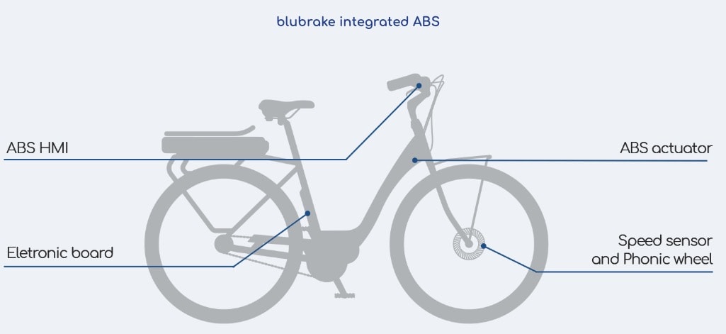
ABS for e-bikes
Blubrake wants your front wheel on an e-bike to have ABS, ensuring a safer cycling experience. The general trend in bikes is to replace rim brakes with disc brakes.
Blubrake min
Sun-powered E-trike
Wello has a hybrid pedal-powered trike that converts sunlight into electricity, giving you a boost.
Bicycle Computer
I’ve used CatEye, Garmin and Wahoo products for road cycling, and success draws competitors. This new computer from Million Concept Electronics is aimed at entry-level cyclists.
Million Concept Electronics – isport (Distance, speed, heart rate)
Bosch showed a new bike computer designed for e-bikes, it even controls a headlight and brake light, has a color display showing motor power versus pedal power, time of day, miles per hour, all sorts of analytics. There’s nothing from traditional bike computer makes like Wahoo, Garmin or CatEye designed specifically for e-bikes.
Kiox from Bosch, for e-bikes
Bio Sensors
Something totally new from Leomo is Type-S, a system with two sensors placed on your thighs and then a display with real-time analytics about how smooth your pedal stroke is, heel movement, even the pelvic angle, rock and rotation. Wow, there isn’t anything else like this in the world, although it’s something that would benefit a bike fitting session for sure.
Leomo min
Gaming Rollers
Real Design Tech has a set of rollers that you ride on, then use your bike to control a gaming joystick, pedals act like shooting controls.
I used my first rollers back in the 1970’s and the trick was how to balance without flying off the sides, because there were no guards to keep you in place. With the RealDesignTech rollers they’ve designed it so that you cannot fall off at all. To be viable they need to have a smart resistance unit and work with Zwift, instead of a proprietary system.
RealDesignTech
https://www.youtube.com/watch?v=lfNW3sqU4I4
Adaptive Suspension
Bumpy roads are the bane of cyclists, so HiRide has come up with electronically-controlled adaptive suspension for both Road and Mountain bikes.
HiRide adaptive suspension
Smart Lock
How about using your fingerprint to open a bike lock? That’s what BenjiLock showed, so no need to remember that key or combination again.
BenjiLock
Smart Glasses
Bosch will tout their Light Drive smart glasses that will help cyclists see more information from a bike computer system.
Light Drive from Bosch
Air-free Tires
I had 21 flats cycling in 2018, so yeah, I’m a bit interested in a flat-proof tire but it has to roll fast.
Bridgestone
Spin Bikes
In 2019 we watched the spin bike company Peleton go IPO and stumble in price, yet this category continues to grow with new entrants. The trainers come with a display and use WiFi to connect to an online instructor or workout sequence.
Myx FitnessEchelon EX 5S Indoor Cycle
You may be wondering what qualifies me to write about cycling, well for 2019 I biked 12,798.9 miles, so follow me on Strava, or let’s go for a ride when you visit Oregon. During the rainy winter months I do some virtual rides indoors on a Tacx Neo 2T smart trainer, using the Zwift app, so follow me: Daniel Payne (VV).
Just finished the 205 mile Seattle to Portland ride
Cybersecurity will be hard pressed to take on the new challenges of bank managed digital currencies.
Banks are developing their own digital currencies. The introduction of Central Bank Digital Currencies (CBDC) is the beginning of an interesting trend that will change the cybersecurity dynamic for banking as it opens up an entirely new threat landscape.
The renowned Bank of England has issued working papers for research on CBDC’s, looking into the value and challenges. At least 18 different centralized banks have indicated they are proceeding with issuing their own sovereign digital currencies. The Block has compiled a list showing several are already launched, while others are in development or pilot phases.
These digital assets will differ from traditional cryptocurrency, but will likely use some form of blockchain ledgers. It is expected the first iterations will be private blockchains, but the underlying technology will likely support the open benefits of public blockchains or hybrid variants for security, access, transparency, and privacy. These new systems will be complex but are intended to usher in a new set of financial services at lower costs to consumers.
There are potentially great benefits for those banks pushing the technology envelope, but there are also risks. I predict each will have a slightly different implementation, but it could foster an environment of competition that sparks rapid innovation across the sector. Such situations are highly beneficial to cybercriminals that are looking for weaknesses they can exploit. In the race to get new features to market, security is often de-prioritized and good cybersecurity practices can be overlooked. This creates higher likelihoods of vulnerabilities that can lead to hacks. Compromising a digital currency, backed by a major banking institution, is a fine target for cybercriminals.
CBDC’s could be great for all consumers but it will likely bring many headaches to the cybersecurity professionals tasked with protecting the new digital assets, infrastructure, and institutional reputations.
For many industrial businesses, 2019 has been tough. Profits lower across the board – light and heavy industry, state-owned and private businesses. Labor costs rising while ex-factory prices are not. Access to debt restricted. The gap between high performers and laggards widened further, with leaders raising capital expenditures 20 percent plus over last year as they double down on deploying robotics, IoT, blockchain, and other productivity enablers in their supply chain. Laggards are edging closer to bankruptcy.
There are strong signs that we will see more bankruptcies in 2020. More banks will be allowed to fail beyond the four shuttered so far in 2019. The PBOC declared in its 2019 Financial Stability Report that it had closed 1000 P2P lenders in 2019 and that they evaluate close to 600 smaller banks (13 percent of the total) as “risky”. Their solution will have “Chinese characteristics”: failing banks will almost all be bailed out through merging with one of China’s larger banks.
More property companies will find they are financially extended beyond the level at which black-market lenders will support them. Industry consolidation will be the main solution. Investors will see more dramatic falls in share prices for specific stressed listed companies in the mainland and Hong Kong, along the lines of the 90 percent plus falls at Kasen, ArtGo and Tibet Water in recent weeks. This is a positive, companies that had been clogging up their sectors are finally being cleared out. Business will need to be alert to the financial state of their customers and suppliers.
High growth sectors in 2020 will be clustered in consumer facing services, many internet-enabled. Healthcare, education, travel, and leisure will all remain strong. Sectors where the Chinese government actively encourages investment have been clearly laid out– from semiconductor, to AI and smart cities, to manufacturing IoT, to biotech and advanced materials. Making money in these sectors directly in the short term may be tough, but making money out of supplying to these sectors can be very attractive.
Hong Kong and business
Hong Kong entered a recession driven by the downturn in tourists (nearly 1 million fewer travelers through Hong Kong airport last month with 20 percent fewer arrivals from mainland China) and by locals pulling back on spending. More than 50 conferences and exhibitions have been postponed or moved elsewhere. Popular hotels and restaurants have utilization down below 40 percent, even with 40-60 percent discounts, and are putting staff on unpaid leave. Retailers from clothing to jewelry have sales down as much as 50 percent from last year.
Businesses clustered in industries in and around the financial markets have been less impacted. Financial markets have not closed and IPOs are still happening. But changes are being considered. While they won’t make overnight changes to a successful operating model, many are now starting to think through the what ifs and could act on them in 2020.
For some multinationals, asking the basic question of why a large regional headquarters is in Hong Kong and why it is of the scale that it is can return slightly uncomfortable answers. For a good number, the answer is little more than it has always been like that – a location decision that was made rationally 20 or 30 years ago had not been challenged since then. Plus their senior executives like the low tax rates on offer in Hong Kong.
For China focused businesses, more regional activity could be undertaken in the mainland, without material additional cost. Asean and North Asian businesses may have grown to the scale to justify their own regional hubs. With mainland visitor numbers to Hong Kong looking unlikely to recover soon, luxury brand businesses are questioning just how many outlets they should retain in Hong Kong.
If clients from the mainland now prefer to meet in Shenzhen, it is straightforward to upgrade a Shenzhen office, to accommodate more permanent staff. Shenzhen or other local governments may even offer GBA policy incentives to do so.
Looking forward into 2020, business leaders in Hong Kong face tough organizational challenges such as sustaining a culture in which mainland and local staff work effectively, and persuading Hong Kong staff to continue to take opportunities in the mainland.
Few corporate leaders in Hong Kong are well prepared for these fundamental people challenges. There will likely be public instances where they fall short in 2020.
Closing
2020 is the final year in China’s decade long challenge to double its GDP. The government will be able to declare success (potentially with a little support from statistical revisions). US tariffs will continue to have minor impact on Chinese growth. Domestic consumption and investment will remain the key economic drivers, and China will deploy targeted stimuli to maintain momentum.
Many businesses will find 2020 a challenging, stressful year in China – more bankruptcies, more regulation, more unpredictable risks to reputation, and more selective consumer consumption. Yet China will only grow in importance to the majority of global businesses – as a source of global demand, of innovation, of capital, and of newly emerged world class competition. In spite of external pressure to deglobalize, global businesses will evolve their supply chain, their operating model, and even their ownership structure if needed to remain relevant in China.
You know that a technology is becoming a trend to watch when the Economist writes a piece on the topic. We know how big an investment goes into monetizing visual content for our phones, pads and TVs, through the likes of Warner Media, Disney and Netflix. Now there’s a big push into monetizing our ears, driven by Apple and others on the hardware side and Spotify and Liberty Media on the content side. The audio market is still much smaller but it’s growing fast. Apple’s AirPods are guessed to be the fastest growing of all its product lines and are expected to top $15B in sales next year. Spotify and others are aggressively expanding in streaming and also, interestingly, podcasts. Podcasts apparently have better economics than music for audio streaming services.
These directions and more are encouraging further advances in connectivity to our ears. The Bluetooth SIG announced at this year’s CES their latest 5.2 advance to the core Bluetooth specification, and a new software framework on top of the standard called LE Audio. Together these offer higher quality at lower power in wireless earbuds, along with some amazing new possibilities.
TWS
I’ve written before on the topic of true wireless stereo (TWS) in earbuds. Pre 5.2, Bluetooth is a single-channel wireless connection. Left and right audio channels must be transmitted together through that one audio channel to one earbud, say the left. From there, the right audio channel is transmitted wirelessly to the right earbud. This runs batteries down faster and introduces a delay between L and R channels. Vendors have built proprietary solutions to overcome the latency problem but they’re a hack and obviously not shareable between different phone models.
5.2 adds isochronous communication channels over BLE so can transmit L and R simultaneously. Latency problem solved, no longer any need to run down earbud batteries in wireless forwarding and the solution is based on a standard so should be shareable between phone and earbud models. This goes further. An additional channel is supported for voice; you can speak at the same time you’re listening. Full duplex conversations through your earbuds!
LE Audio
The Bluetooth SIG has bigger ambitions still. LE Audio is a software framework on top the core standard; it is expected to be ratified some time in 2020. It adds a new LC3 codec, allowing for tuning between audio quality and power and enabling higher quality than the existing standard, when appropriate.
LE Audio supports many-to-one and one-to many connections. You can connect to multiple sources: a music player, your phone and a TV, and be able to switch between these, even allowing all to be active simultaneously, one dominant and the others turned down. For one-to-many, you can share your audio stream with others. You’re listening to a great song and want your friends to hear it too? Just share the stream. Or you can all watch a video on a phone or laptop while each enjoying a direct audio stream to your own earbuds.
Here’s another cool thing you’ll be able to do. You’re at a sports bar, lots of screens showing lots of games, but all silently. It would be a mess if the audio from each was playing at the same time, right? You walk into the bar, see a game that interests you and grab the audio stream from that game. Now you can watch and listen. Or you’re in an airport departure lounge, trying to keep up to date on messages that might affect you flight. This is the reverse of the sport bar. Announcements in airports are all full volume, overlapping and competing for your attention. Wouldn’t it be nice to be able to grab an audio stream for announcements just on your flight? And turn all those loudspeakers off?
There’s good news also for hearing-aid users. With these kinds of capabilities, they should be able to better hear suitably-equipped speakers in presentations and in other noisy surroundings.
CEVA is a broad-line supplier for Bluetooth solutions including Low Energy (supporting LE Audio) and Dual Mode (supporting Classic Audio and LE Audio). They also provide a wide range of related audio solutions: voice pickup, VAD, audio input and beamforming, AEC and ANC and speech recognition. And they provide solutions for gestures detection. taps, head movements. You can learn more about the Bluetooth platforms HERE and audio, voice and speech solutions HERE.
Fisita World Mobility Summit 2019 in Nagoya, Japan, brought together powerful perspectives on everything from vehicle architectures (Visteon), to open source software (Synopsys), mobility (METI), and connectivity (Bosch). The most enigmatic juxtaposition at the event, however, came in a panel discussion I moderated between General Motors’ Vice President, Global Electrification, Controls, Software and Electronic Hardware, Dan Nicholson, and Dr. Kazunari Sasaki, professor (hydrogen energy systems) and senior vice president, Kyushu University.
These two executives stand at the fulcrum of vehicle propulsion facing tectonic forces tearing at the automotive industry. For Professor Sasaki, residing as he does in the energy desert of Japan, hydrogen is the future – promising a clean, energy independent path to future mobility.
For Mr. Nicholson of GM, all roads lead away from proven profitable propulsion technologies such as diesel and internal combustion engines. The third slide Nicholson showed in his presentation was of a diesel-powered, extended-cab Chevrolet pick-up truck towing a massive trailer. His fifth slide was an artist’s rendering of GM’s new global electric vehicle platform.
The existential crisis posed by these two perspectives is hard to ignore. For Sasaki, the choice of hydrogen is clear, clean, and rational if not downright essential. As noted by a Toyota Advanced Development (AD) executive, James Kuffner, in the closing presentation of the Fisita event: “Hydrogen has an energy density that is 3x higher than gasoline and an overall higher maximum efficiency. If you combine a hydrogen fuel cell with an electric motor, the efficiency is 2x or 3x more efficient than a conventional gas engine.”
Sasaki was also quick to note that hydrogen is the most abundant element in the universe and that the primary byproduct of the hydrogen energy cycle is water vapor. When put this way, opponents of hydrogen would appear to be either ignorant or foolish – or “fuelish” to borrow Tesla Motors’ CEO Elon Musk’s disparaging assessment of hydrogen’s prospects.
For Nicholson, GM is in the midst of a massive corporate pivot away from smaller passenger cars toward crossovers and SUVs, away from internal combustion engines to electric powertrains, and away from human-centric driving to autonomy. This is Clayton Christensen’s “creative destruction” on steroids threatening 40% of the legacy ICE supply chain and a good portion of the vehicle assembly workforce – painful for GM having just recently concluded a month-long UAW strike.
Unfortunately for Nicholson the Fisita event occurred prior to GM’s latest earnings report and before the company announced plans for a new EV battery assembly plant (a joint venture with LG Chem) in Lordstown along with its intentions to build an EV pickup truck in Hamtramck by 2021. As a result, Nicholson was noncommittal as to the timing of GM’s wider deployment of EV technology.
What is clear, though, is that the shift to EV technology, by Nicholson’s own description, has significant implications for the role of software and connectivity in future electrified vehicles. These implications are touching the entire architectural underpinnings of the vehicle – which was reflected in the domain consolidation strategy described by Markus Schupfner, senior vice president and chief technology officer for Visteon speaking at the Fisita Summit.
As bleak (and promising) as the picture may be for a legacy ICE-oriented manufacturer like GM, the prospects for the promoters of hydrogen are more grim and hold important lessons for auto makers. The merits of hydrogen propulsion are both indisputable and debatable – and they are likely to be debated until that massive ball of hydrogen and helium in the sky implodes.
The automotive poster child for hydrogen propulsion is Toyota’s Mirai. This vehicle offers an important example of both the lengths and limits to which an automobile company can stretch to promote a vehicle it desperately wants to be successful – in the face of massive consumer indifference.
After four years, Toyota claims to have put 6,000 hydrogen-powered Mirai’s on the road in the U.S. These have been hard won sales with a range of consumer incentives including:
· A complimentary fuel cell card worth $15,000
· $2,500 in loyalty cash
· $7,500 in bonus cash
· 1.9% financing for 72 months
The incentives are necessary given the limits of the current network of fueling stations confined mainly to California. The limits of existing fueling options and the weakness of the current hydrogen infrastructure was made clear when a catastrophic fire and explosion occurred at an Air Products hydrogen plant in Santa Ana, California, in June of this year knocking out hydrogen supplies for Northern California for five months.
The Air Products disaster forced owners of hydrogen-fueled vehicles to idle or trade them in. (The high cost of luxury car insurance was noted by some as a reason for turning their cars in. Toyota representatives said the company took on the lease or financing payments for some Mirai owners.)
The developments in California could and should be seen by many as the end of the hydrogen car conversation in the U.S. Hydrogen may make sense for commercial vehicles and public transportation, but the vulnerability of an already fragile and fledgling charging network is likely to be too much for even the greenest of green-leaning car buyers to tolerate. There are two valuable takeaways here.
First, California, like Japan, has geographic and geologic reasons for taking a regulatory interest in the automotive market. Both Japan and California are concerned about emissions. But Japan has an abiding interest in energy independence and California has a perpetual struggle with air quality.
These circumstances of geography give both regions common cause to promote both electrification and hydrogen fuel technologies. California has been willing to put its thumb on the scale for electrification with stringent emissions and fuel efficiency standards – but neither Japan nor California have provided incentives for hydrogen-fueled vehicles.
This has put companies like Toyota, Hyundai, and Honda in the awkward position of advertising, promoting, and selling hydrogen-powered cars that may be green but are complicated and expensive to operate from a cost, charging, and insurance standpoint. The array of incentives offered by Toyota on the Mirai represent a case study in how a car company tries to sell a car against the headwinds of consumer indifference.
It is instructional to compare the enthusiastic funding of charging and the range of discounts and discounted financing Toyota is offering for the Mirai against the lack of aggressive promotional activity by BMW, Cadillac, Chevrolet, Nissan, Mitsubishi, and other auto makers for their electric vehicles.
I can remember visiting local Chevrolet dealers in the earliest days of the Volt extended range electric vehicle and finding the car being offered at a premium price with dealers claiming ignorance of a well-documented low-cost lease option. The Volt met its demise in early 2019 and GM expects to sell a measly 20,000 Bolt EVS annually. It’s hard to get excited about a car when you lose money on every one you sell.
It’s clear that the Bolt is being allocated sparse marketing dollars. I can’t say that I’ve ever seen a television advertisement or a dealer-advertised incentive offer for a Bolt. The vehicle is increasingly looking like a gig-economy fleet offering for the foreseeable future.
Comparing the promotional effort applied to the Mirai by Toyota and the paucity of promotion allotted by the legacy ICE-based vehicle makers for EVs, it is easy to see why Tesla has scampered away with the lion’s share of the EV market and is threatening the sales leadership of traditional ICE-based luxury cars. Car companies are refusing to back up their nascent EV efforts with muscular marketing campaigns.
The latest losers (in the estimation of automotive journalists and some analysts) have been Audi’s E-tron and Jaguar’s I-pace – both posting a few thousand vehicle sales in their first months on the U.S. market in the face of more than 111,000 Tesla Model 3 sales. Alternative propulsion technologies, whether electric or hydrogen-based, remain an awkward talking point for auto makers.
Key takeaways are that car buying decisions remain emotional – not rational. The biggest challenge isn’t making the cars that people want, it is making people want the cars that have been made. Alone among EV auto makers, Tesla appears to be making the cars that people want. It remains one of the few car makers if not the only one struggling to keep pace with advance orders.
The real challenge for Tesla’s EV rivals like General Motors may not be the electrical architecture of their vehicles. It will be rewiring their marketing and dealer networks to support and promote EV-based vehicles.
When describing the complexity of deep sub-micron systems on chip (SoCs), most engineers and their managers tend to refer to a combination of gate count, amount of embedded memory, and frequency of operation. If one’s task is to assess the complexity of the physical design effort for a given SoC, then there are numerous additional factors that can create challenges far more significant than the sheer size or frequency of the design.An example of one such SoC is clearly illustrated by recent experience in performing the physical design work for a customer’s SoC project. Traditionally focused its efforts on very large SoC designs, usually containing many millions of gates, megabits of memory distributed over hundreds of individual RAMs, and with frequencies of operation well over 200 MHz. In contrast, this customer’s design had less than one million gates of logic. It had about 500 kilobits of embedded memory spread over 23 standard RAMs plus 6 megabits of memory in a single MoSys 1-T SRAM. Its primary frequencies of operation were 162 MHz and 81 MHz. From these statistics alone, most physical design engineers would not consider this SoC to be extremely challenging, yet when one looks into the next level of details the unique challenges become apparent.
Small Chip, Big Constraints
This specific SoC was the second chip of a two-chip set. This situation forced certain constraints upon the design that were non-negotiable.
The biggest constraints were with respect to functional I/O locations, and specifically, the LVDS (Low Voltage Differential Signaling) interface. The LVDS interfaces on both chips and the board were designed such that the two chips’ LVDS interfaces would basically abut. This constraint provided no latitude on where the LVDS I/O pads could be located.
Being differential, these I/O pads were very wide and occupied the majority of one side of the chip. From a timing perspective, the first chip and board consumed the majority of the available timing budget for the LVDS interface. This imposed a very tight data valid window and, hence, an extremely tight clock skew requirement on the interface.
Besides I/O location, minimum area was another major constraint of the design. While certainly a common constraint for most SoCs, this chip had a single memory that occupied half the active area. This essentially locked the dimension of the chip in both directions; the X direction was determined by the width of the MoSys RAM, the Y direction by the overall area limit for the design. This forced all other components into a very small, very dense fixed size region. This region had to include three mixed signal components, 23 embedded RAMS, and a CPU.
The floorplanning options of this region were quite limited. The fixed positions of the I/O largely fixed placement of the associated mixed signal components. Additionally, the mixed signal components had a large “keep out” area where standard cells, macros, and routing were not allowed. The embedded RAMs needed to be placed such that the design was routable, while avoiding the mixed signal components and yet fitting into the available X and Y dimensions.
Together these factors compressed the area available for the core logic and increased the already high utilization. In such situations designers need to quickly explore floorplan alternatives. The floorplan in subsequent iterations could be easily modified , GDS Builder, can place objects relative to other objects or reference points (for instance, place macro2’s lower left corner next to, or a certain distance from, macro1’s lower right corner). GDS Builder was used to automate chip construction.
GDS Builder automatically kicked off Synopsys AstroExpress place and route jobs, as well as timing, IR drop and electromigration analysis on the entire design overnight. Overnight full-chip builds enabled us to explore the multiple floorplanning alternatives using the production placer and router. In doing so we came up with the optimal floorplan that met all the constraints implied by the design. There was 100 percent timing and area correlation between these early floorplan explorations and the final taped out chip.
Mountains and boulders
Hard macros are a constant source of distress for physical design engineers for a variety of reasons. In very large SoC designs, there can be a good deal of flexibility where these macros are placed in order to create an optimal floorplan. In the case of this design, there were a large number of hard macros that needed to be placed in a very small area.
The largest of these macros was the MoSys 1-T embedded memory that occupied half the active area of the chip. If the other embedded memories were considered to be boulders in the sea of standard cells, the MoSys memory would then be a mountain. Although signals between the I/O pads and standard cell core could be routed over the MoSys memory, it was too large a distance to go without buffering the signals. The only choice was to go around the MoSys memory, leaving narrow tracks along the top and the sides of the memory where GDS Builder’s automated repeater insertion could place appropriate buffers along the way from the I/O pads to the standard cell core.
Power distribution also proved to be a challenge with respect to the MoSys memory. Core power had to be routed from the top of the die over the MoSys to the standard cell core. Metal layers 5 and 6 were mostly available for this purpose, but with some irregularly placed obstructions. This forced us to construct a customer power cover cell that fed the standard cell core with adequate power. The adequacy of this power strategy with respect to IR drop and electromigration was then verified using Astro-Rail.
One of the advantages from a system perspective of using MoSys memories is the high density and wide parallel data interface. From a physical design perspective, however, the wide interface also creates a significant amount of routing congestion near the data pins. To avoid this congestion, placement obstructions for standard cells had to be created. This, of course, required even higher utilization to be achieved in the standard cell core area.
Placing the I/Os
Our example SoC had only 246 total bond pads. This number is considered relatively small by today’s standards, yet this pad ring proved to be one of the greatest challenges of the design. To begin with, there were four different I/O libraries utilized. The first library was chosen to minimize die size since it had low profile standard I/O cells with integrated bond pads.
The second I/O library was required for the LVDS interface. It contained high profile and large width cells that did not include bond pads. To accommodate non-LVDS I/O adjacent to LVDS cells, a third library was required. This was a high profile library with narrow pitch and non-integrated bond pads. The fourth I/O library was for analog I/O and was also high profile.
Cells from different libraries with differing heights were mixed on the same side of the chip. This forced the creation of special filler and corner cells to interface between the different height cells. Special consideration was required as to how the different height I/O power pads were to connect to the internal power grid. Figure 1 shows the transition from the low profile I/O cell to the high profile I/O cell through a custom filler cell. The special connections from the low profile I/O cell power pads to the core power ring are also visible.
To further complicate matters, there were seven distinct power domains associated with the I/O ring. These domains were for the LVDS interface, the various analog domains, and the primary 3.3 volt and 1.8 volt power domains.
The LVDS portion of the pad ring proved to be especially challenging. As these signals were the most timing sensitive in the design, it was decided to place LVDS related “edge logic” in the actual pad block that contained the LVDS I/O pads. This approach allowed us to meet a very restrictive timing budget required by the customer.
Smaller is not always easier
As you consider your next SoC project, it is important to look beyond the obvious metrics such as gate count and frequency when estimating the complexity, effort, and schedule required for physical design. Factors such as I/O complexity, the use of unique IP, and number of constraints imposed on the design can play a major role in determining the effort and schedule of a complicated SoC, whether it is considered to be a large or small design.


