RVN! 26 Banner revised (800 x 100 px) (600 x 100 px)

The Practitioners View of DAC – Design, IP and Embedded

The Practitioners View of DAC – Design, IP and Embedded
by Mike Gianfagna on 12-07-2020 at 10:00 am

The First DAC

Next year will mark the 58th year for the Design Automation Conference. It’s hard to wrap your head around the fact this event dates back to 1964, when rock ‘n roll was new, cars were big and computers were even bigger. In its early days, the event was called the Design Automation Workshop. Pictured above is the cover of the very first proceedings. It’s no longer available on Amazon unfortunately. Throughout its storied life, DAC has presented some of the most advanced and important innovations that have shaped the technology world around us. The conference began and continues today as a place to present high quality, cutting edge research. Over the years, exhibits were added to showcase the results of this research. More recently, a series of tracks were added that showcase the practitioners view of DAC – design, IP and embedded. I’d like to focus on this part of the conference.

Ambar Sarkar, Ph.D., NVIDIA Inc.

The Designer and IP tracks have been part of the DAC program since 2010. The Embedded track was added last year. Putting on DAC is a huge undertaking and a great deal of the work involved is done by a group of volunteers from industry and academia. Their willingness to give back is truly noteworthy. I recently had a chance to chat with one of those folks – Ambar Sarkar from NVIDIA, who is the chair for the Designer IP and Embedded tracks on the DAC Executive Committee.

Ambar began by explaining the structure of this part of the DAC program. There are front-end and back-end Designer tracks as well as an IP track and an Embedded systems track. Each track contains submitted work as well as special invited sessions. In reality, there is some grey area between front-end/back-end and IP design which is fine. Ambar chairs a committee that helps to sort all this out. You can learn more about the workings of the IP committee in this interview I did with Randy Fish. You can see who’s who on the DAC Executive Committee here.  

I spent a bit of time discussing the submitted work portion of these tracks with Ambar. As I mentioned earlier, DAC is a high-profile, prestigious place to present your work. It is highly regarded, and the work presented at DAC is often cited and used broadly in semiconductor and EDA. The Designer, IP and Embedded tracks share this spotlight, but there is an important difference. Submitting a technical paper to the DAC Research track takes a fair amount of work. The final submission includes a technical manuscript and a presentation, with peer-review vetting along the way. The deadline for submitting a technical paper to the Research track has already passed. The deadline is traditionally in November of each year.

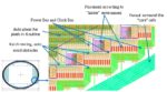
In 2020, overall submissions to the Designer and IP tracks rose 15%, continuing a steady three-year rise: 160 paper submissions in 2018, 170 in 2019 and 197 in 2020.  This blog post will provide more information on the 2020 Designer and IP track submission trends.  Ambar said he is confident there will continue to be a rise in submissions in these tracks. 

The requirements for submission to the Designer, IP and Embedded tracks is a bit different. Here, an abstract of approximately 100 words and up to six PowerPoint slides are needed and the submission deadline is later than the Research track.  Submissions are peer-reviewed by a number of industry/domain experts to ensure quality, but the submission process for this part of the conference has been streamlined. In spite of the simpler process, I can tell you the work presented at these tracks receives a lot of attention due to the very high-quality technical content. Over the years, I have been involved in many Designer track and IP presentations and it has been a very rewarding experience.

Consider that the development of new IP along with its software and integrating it into a new SoC is a fundamental innovation engine for the semiconductor industry. The Designer, IP and Embedded tracks provide a spotlight on that work at a very high-profile conference. If you’re proud of something you’ve worked on this past year with a customer or internally at your company, you should definitely consider a submission.  The work is reasonable, and the reward is significant.

Submissions to these tracks are open now.  The deadline for submission is January 20, 2021. Think about what you’d like to present and submit a proposal before the holidays. You’ll be notified of acceptance between March 10 and 18, 2021. There are clear instructions on how to submit your work on the DAC website, including a detailed outline for how to develop your six slides. Past companies who presented are also shown there. It’s quite an impressive list.  You want to be on that list. Here are the links:

Check it out to learn about the practitioners view of DAC – design, IP and embedded.


How Intel Stumbled: A Perspective from the Trenches

How Intel Stumbled: A Perspective from the Trenches
by Daniel Nenni on 12-07-2020 at 6:00 am

Stacy and Bob Intel SemiWiki

Bloomberg did an interview with my favorite semiconductor analyst Stacy Rasgon on “How the Number One U.S. Semiconductor Company Stumbled” that I found interesting. Coupled with the Q&A Bob Swan did at the Credit Suisse Annual Technology Conference I thought it would be good content for a viral blog.

Stacy Rasgon and Bob Swan

Stacy Rasgon is an interesting guy and a lot like me when it comes to offering blunt questions, observations, and opinions that sometimes throw people off. As a result, Stacy is not always the first to ask questions during investor calls and sometimes he is not called on at all which is the case for the most recent Intel Call.

Stacy is the Managing Director and Senior Analyst, US Semiconductors, for AB Bernstein here in California. Interestingly, Stacy has a PhD in Chemical Engineering from MIT, not the usual degree for a sell side analyst. Why semiconductors? Stacy did a co-op at IBM TJ Watson Research Center during his post graduate studies and that hooked him.

I thought it was funny back when Brian Krzanich (BK) was CEO of Intel. BK has a Bachelor’s Degree in Chemistry from San Jose State University and he was answering questions by an analyst with a PhD from MIT. The current Intel CEO Bob Swan is a career CFO with an MBA so maybe that explains the communication issues.

In the Bloomberg interview the focus was on the delays in the Intel processes starting with 14nm, 10nm, and now 7nm. Unfortunately they missed the point. In the history of the semiconductor industry leading edge processes were more like wine where in the words of the great Orson Wells “We will sell no wine before its time”. Guided by Moore’s Law, Intel successfully drove down the bumpy process road until FinFETs came along.

The first FinFET Process was Intel 22nm which was the best kept secret in semiconductor history. We don’t know if it was early or late since it was not discussed before it arrived. 14nm followed which was late due to defect density/yield problems. We talked about that on SemiWiki quite and I had a bit of a squabble with BK at a developer conference. I knew 14nm was not yielding and he said it was only to retract that comment at the next investor call. Intel 10nm is probably the most tardy process in the history of Intel and now 7nm is in question as well.

The foundries historically have been 1-2 nodes behind Intel so they got a relative pass on being late with new processes up until 10nm when TSMC technically caught Intel 14nm.

Bottom line: Leading edge processes use new technology and materials which challenges yield from many different directions. This is a very complex business so it’s extremely difficult to predict schedules because “you never know until you know”. So, try as one might, abiding by Moore’s Law in the FinFET era is a fool’s errand, absolutely.

The other major Intel disruption is the TSMC / Apple partnership. Apple requires a new process each year which started at 20nm (iPhone6). As a result TSMC now does half steps with new technologies. At 20nm TSMC introduced double patterning then added FinFETs at 16nm. At 7nm TSMC later introduced limited EUV and called it 7nm+. AT 5nm TSMC implemented full EUV (half steps).

This is a serious semiconductor manufacturing paradigm shift that I call “The Apple Effect” TSMC must have a new process ready for the iProduct launch every year without fail. Which means the process must be frozen at the end of Q4 for production starting in the following Q2. The net result is a serious amount of yield learning which results in shorter process ramps and superior yield.

The other interesting point is that during Bob Swan’s Credit Suisse interview he mentioned the word IDM 33 times emphasizing the IDM advantage over being fabless. Unfortunately this position is a bit outdated. Long gone are the days when fabless companies tossed designs over the foundry wall to be manufactured.

TSMC, for example, has a massive ecosystem of partners and customers who together spend trillions of dollars on research and development for the greater good of the fabless semiconductor ecosystem. There is also an inner circle of partners and customers that TSMC intimately collaborates with on new process development and deployment. This includes Apple of course, AMD, Arm, Applied Materials, ASML, Cadence, and Synopsys just to name a few.

Bottom line: The IDM underground silo approach to semiconductor design and manufacture is outdated. It’s all about the ecosystem and Intel will learn this first hand as they increasingly outsource to TSMC in the coming process nodes.


Quantum Internet Explained

Quantum Internet Explained
by Ahmed Banafa on 12-06-2020 at 10:00 am

Quantum Internet Explained

Building a quantum internet is a key ambition for many countries around the world, such a breakthrough will give them competitive advantage in a promising disruptive technology, and opens a new world of innovations and unlimited possibilities.

Recently the US Department of  Energy (DoE) published the first blueprint of its kind, laying out a step-by-step strategy to make the quantum internet dream come true,. The main goal is to make it impervious to any cyber hacking. It will “metamorphosize our entire way of life,” says the Department of Energy. Nearly $625 million in federal funding is expected to be allocated to the project.

A quantum internet would be able to transmit large volumes of data across immense distances at a rate that exceeds the speed of light. You can imagine all the applications that can benefit from such speed.

Traditional computer data is coded in either zeros or ones. Quantum information is superimposed in both zeros and ones simultaneously. Academics, researchers and IT professionals will need to create devices for the infrastructure of quantum internet including: quantum routers, repeaters, gateways, hubs, and other quantum tools. A whole new industry will be born based on the idea of quantum internet exists in parallel to the current ecosystem of companies we have in regular internet.

The “traditional internet “, as the regular internet is sometimes called, will still exist. It is expected that large organizations will rely on the quantum internet to safeguard data, but that individual consumers will continue to use the classical internet. [1]

Experts predict that the financial sector will benefit from the quantum internet when it comes to securing online transactions. The healthcare sectors and the public sectors are also expected to see benefits. In addition to providing a faster, safer internet experience, quantum computing will better position organizations to solve complex problems, like supply chain management. Furthermore, it will expedite the exchange of vast amounts of data, and carrying out large-scale sensing experiments in astronomy, materials discovery and life sciences [1][3]

But first let’s explain some of the basic terms of the quantum world: Quantum computing is the area of study focused on developing computer technology based on the principles of quantum theory. The quantum computer, following the laws of quantum physics, would gain enormous processing power through the ability to be in multiple states, and to perform tasks using all possible permutations simultaneously. [2]

A Comparison of Classical and Quantum Computing

Classical computing relies, at its ultimate level, on principles expressed by a branch of math called Boolean algebra. Data must be processed in an exclusive binary state at any point in time or bits. While the time that each transistor or capacitor need be either in 0 or 1 before switching states is now measurable in billionths of a second, there is still a limit as to how quickly these devices can be made to switch state. As we progress to smaller and faster circuits, we begin to reach the physical limits of materials and the threshold for classical laws of physics to apply. Beyond this, the quantum world takes over. [2]

In a quantum computer, a number of elemental particles such as electrons or photons can be used with either their charge or polarization acting as a representation of 0 and/or 1. Each of these particles is known as a quantum bit, or qubit, the nature and behavior of these particles form the basis of quantum computing. [2]

Quantum Superposition and Entanglement

The two most relevant aspects of quantum physics are the principles of superposition and entanglement.

  • Superposition: Think of a qubit as an electron in a magnetic field. The electron’s spin may be either in alignment with the field, which is known as a spin-up state, or opposite to the field, which is known as a spin-down state. According to quantum law, the particle enters a superposition of states, in which it behaves as if it were in both states simultaneously. Each qubit utilized could take a superposition of both 0 and 1.
  • Entanglement: Particles that have interacted at some point retain a type of connection and can be entangled with each other in pairs, in a process known as correlation. Knowing the spin state of one entangled particle – up or down – allows one to know that the spin of its mate is in the opposite direction. Quantum entanglement allows qubits that are separated by incredible distances to interact with each other instantaneously (not limited to the speed of light). No matter how great the distance between the correlated particles, they will remain entangled as long as they are isolated.

Taken together, quantum superposition and entanglement create an enormously enhanced computing power. Where a 2-bit register in an ordinary computer can store only one of four binary configurations (00, 01, 10, or 11) at any given time, a 2-qubit register in a quantum computer can store all four numbers simultaneously, because each qubit represents two values. If more qubits are added, the increased capacity is expanded exponentially. [2]

What is Quantum Internet

The quantum internet is a network that will let quantum devices exchange some information within an environment that harnesses the odd laws of quantum mechanics. In theory, this would lend the quantum internet unprecedented capabilities that are impossible to carry out with today’s web applications. [3]

In the quantum world, data can be encoded in the state of qubits, which can be created in quantum devices like a quantum computer or a quantum processor. And the quantum internet, in simple terms, will involve sending qubits across a network of multiple quantum devices that are physically separated. Crucially, all of this would happen thanks to the wild properties that are unique to quantum states. [3]

That might sound similar to the standard internet. But sending qubits around through a quantum channel, rather than a classical one, effectively means leveraging the behavior of particles when taken at their smallest scale – so-called “quantum states”.[3]

Unsurprisingly, qubits cannot be used to send the kind of data we are familiar with, like emails and WhatsApp messages. But the strange behavior of qubits is opening up huge opportunities in other, more niche applications. [3]

Quantum Communications

One of the most exciting avenues that researchers, armed with qubits, are exploring, is communications security.[3]

Quantum security leads us to the concept of quantum cryptography which uses physics to develop a cryptosystem completely secure against being compromised without knowledge of the sender or the receiver of the messages.

Essentially, quantum cryptography is based on the usage of individual particles/waves of light (photon) and their intrinsic quantum properties to develop an unbreakable cryptosystem (because it is impossible to measure the quantum state of any system without disturbing that system.) [4]

Quantum cryptography uses photons to transmit a key. Once the key is transmitted, coding and encoding using the normal secret-key method can take place. But how does a photon become a key? How do you attach information to a photon’s spin? [4]

This is where binary code comes into play. Each type of a photon’s spin represents one piece of information — usually a 1 or a 0, for binary code. This code uses strings of 1s and 0s to create a coherent message. For example, 11100100110 could correspond with h-e-l-l-o. So a binary code can be assigned to each photon — for example, a photon that has a vertical spin ( | ) can be assigned a 1.

Regular, non-quantum encryption can work in a variety of ways but generally a message is scrambled and can only be unscrambled using a secret key. The trick is to make sure that whomever you’re trying to hide your communication from doesn’t get their hands on your secret key. But such encryption techniques have their vulnerabilities. Certain products – called weak keys – happen to be easier to factor than others. Also, Moore’s Law continually ups the processing power of our computers. Even more importantly, mathematicians are constantly developing new algorithms that allow for easier factorization of the secret key. [4]

Quantum cryptography avoids all these issues. Here, the key is encrypted into a series of photons that get passed between two parties trying to share secret information. The Heisenberg Uncertainty Principle dictates that an adversary can’t look at these photons without changing or destroying them. [4]

 Ahmed Banafa, Author the Books:

Secure and Smart Internet of Things (IoT) Using Blockchain and AI

Blockchain Technology and Applications

Read more articles at: https://ahmedbanafa.blogspot.com/

References

[1] https://www.cybertalk.org/2020/10/23/quantum-internet-fast-forward-into-the-future/

[2] https://www.bbvaopenmind.com/en/technology/digital-world/quantum-computing/

[3] https://www.zdnet.com/article/what-is-the-quantum-internet-everything-you-need-to-know-about-the-weird-future-of-quantum-networks/

[4] https://ahmedbanafa.blogspot.com/2014/06/unde


The Future of Connected Car Advertising

The Future of Connected Car Advertising
by Roger C. Lanctot on 12-06-2020 at 6:00 am

The Future of Connected Car Advertising

“Ads definitely work, but we can’t tell you how or why or give you any evidence,” – Tim Hwang, research fellow, Georgetown Center for Security and Emerging Technology

Two recent episodes of the Freakonomics Radio podcast tackle the question “Does advertising actually work?” and they coincided with a presentation given earlier this year by General Motors that attempted to take on the same question. While the podcasts were looking at all forms of advertising, the GM presentation at the Advertising Research Foundation this Fall garnered attention and praise for attacking the question of radio advertising efficacy in connected cars.

Freakonomics podcasts:

https://freakonomics.com/podcast/advertising-part-1/

https://freakonomics.com/podcast/advertising-part-2/

The podcasts highlight the estimated $250B spent on advertising in the U.S. and $600B globally and raise questions regarding the return on investment for all types of advertising and the long-term viability of the advertising-based Internet economy currently dominated by ad-centric powerhouses Google and Facebook. The takeaway from the two discussions is that advertising is performing a difficult to measure function and that participants in the advertising infrastructure are least likely to probe too deeply to question its usefulness.

In that context, the GM insights were most welcome. For its part, GM is one of the largest advertisers in the U.S., spending an estimated $3B. GM must know a lot about advertising effectiveness and, as a major advertiser, commanded the attention of ARF attendees with its analytical look at a radio advertising campaign by Taco Bell.

The focus of the Taco Bell study was to assess the effectiveness of radio advertising in cars. GM created geo-fences around 78 Taco Bell locations in Columbus, Ohio, and then compared vehicle location data with radio ad logs to assess reach and frequency. The entry of cars into the designated geo-fenced store “polygons” was used to determine attribution.

Attribution is the Holy Grail of any advertising analysis – i.e. the attribution of a consumer behavior such as a store visit or purchase that can be directly attributed to a particular advertisement. Of course, to achieve actual attribution would require mind reading or some sort of comprehensive surveillance (coming soon from Amazon or Google, no doubt), but the novelty of using connected car technology to close this analytical loop was impressive if filled with some obvious flaws.

GM’s conclusions were somewhat inconclusive to whit:

  • The typical :30 second radio ad was the most effective in driving restaurant visits.
  • Voiced (personality sponsorships) and NWT (News/Weather/Traffic) ad units generate synergies when combined.
  • The combination of the :30 second standard ads with voiced personality enhanced campaign frequency
  • Mid-day recorded the highest driving activity.

Of the study, GM said: “While the pilot’s results were promising, there’s opportunity to enrich the insights.” In other words, the findings, which oddly included demographic breakdowns, were merely interesting.

The technology behind the study originated with a small startup called Drive Time Metrics. Drive Time Metrics, which holds a number of patents on its work, demonstrated to GM and other auto makers several years ago the ability to obtain a comprehensive view of content consumption in vehicles thereby setting the stage for connected car audience measurement. The two companies do not appear to be currently working together.

The Drive Time endeavor might seem to be nearly meaningless or pointless given the fact that cars spend 97% of their time – or more – parked. Why would media consumption in a connected car matter? It matters because researchers estimate that 50% or more of total radio listening occurs in cars.

More importantly, a listener in a car represents a captive audience and is likely on the way to conducting a transaction of some sort. I like to say that the car itself is the equivalent of a browser and every action of the driver is an indication of intent – purchasing or otherwise.

The only problem for researchers has been that the leading media measurement company, Nielsen Media, has no means for measuring in-vehicle media consumption with any detail or reliability – even though it purports to report total projected radio listening audience data.  This means that big advertisers like GM and advertising-centric companies like Google and Facebook are faced with a major media blindspot – the automobile.

Further, the car is an aural environment. It is nearly impossible, if not dangerous, to leverage visual advertising to target drivers with the possible exception of billboards.

Drive Time Metrics raised the curtain on in-vehicle media measurement by tapping into the vehicle CAN bus – the on-board network – where the company found comprehensive insights regarding what drivers were listening to and from which source. Drive Time’s solution is able to tell auto makers and advertisers what media sources are being accessed, when, where, by whom, and in what car.

In the past, companies such as Harman International have demonstrated in-vehicle ad solutions capable of linking broadcast radio ads from digital or streaming radio sources requiring an action by a driver to obtain a coupon or discount. This crude form of attribution is evident in GM’s Marketplace app developed with Xevo.

This was the very message taken away by some observers at the ARF event. Forbes magazine quoted one “futurist” as saying: “In order to provide radio breakthroughs across more product categories, expect to soon see voice command added to connected cars so drivers with their hands on the wheel can accept radio-advertised coupon and other offers to be downloaded into their phones. At least two different companies are already thinking along those lines, WiO and Thinaire.”

WiO and Thinaire are not alone, but there is nothing new in what they are working on and others have tried and failed before them.

It’s precisely the WRONG message to derive from GM’s presentation. GM’s analysis only gave further evidence of the difficulty of establishing attribution of a particular event to a particular ad. The last thing auto makers ought to be spending their money on is distracting drivers with location-centric advertising with an urgent call to action while driving. This is one thing that GM’s attorneys and engineers ought to be able to agree on.

That intensive form of driver engagement – requiring a screen touch or voice response – is sub-optimal from a driver distraction standpoint. Drive Time’s vision is to open the door to a comprehensive view of the in-vehicle media landscape and with that a projectable audience measurement platform.

The GM presentation is tantalizing but ultimately disappointing and pointless. Advertisers are not interested in understanding the efficacy of radio advertising in GM vehicles. They want to know the efficacy of radio advertising more broadly and in the context of a comprehensive advertising portfolio.

What GM is failing to recognize is that its first goal ought to be to use Drive Time’s technology to better understand its own customers, leveraging those insights to refine GM’s own marketing programs and tune up its in-vehicle infotainment systems. GM is a major radio advertiser both directly and through dealer co-op advertising. GM should go back to the drawing board to better understand how it can apply its newly found insights in support of its own marketing and product development objectives.

As for Drive Time Metrics, all car makers ought to take a closer look at the DTM solution. We will all benefit from better understanding in-vehicle media consumption. Understanding that behavior will help user experience designers create non-distracting solutions for the next generation of non-distracting in-motion marketing.


CEO Interview: Tony Pialis of Alphawave IP

CEO Interview: Tony Pialis of Alphawave IP
by Daniel Nenni on 12-04-2020 at 10:00 am

Tony Pialis Alphawave on SemiWiki

Tony Pialis is a visionary entrepreneur focused on developing
technologies for next generation connectivity. In the last twenty 20 years, he has co-founded three semiconductor IP companies, all exclusively targeting connectivity IP. Tony is currently the CEO of Alphawave IP Inc, a leader in delivering multi-standard wireline IP for AI, datacenter and 5G networks.

Starting in 1999, Tony was an early founder of Snowbush
Microelectronics Inc, a Canadian-based analog design services and IP organization that subsequently became a leading supplier of analog and mixed-signal IP cores. Snowbush was acquired by Gennum/Semtech in 2007 and is currently part of Rambus.

In 2008, Tony founded V Semiconductor, where he served as President and CEO. V Semiconductor was a leader in delivering 10Gbps Ethernet and PCI-Express Gen3 IP solutions to top tier semiconductor manufacturers. In 2012, Intel acquired V Semiconductor Inc.

At Intel, Tony was the Vice President of Analog and Mixed-Signal IP. His organization was responsible for developing analog IP portfolios for both networking/datacenter and portable devices. During his tenure at Intel, Tony and his organization won the prestigious Intel Achievement Award for successfully delivering next generation Ethernet and PCI-Express SerDes solutions on Intel’s 22nm and 14nm process technologies.

Tony earned bachelor’s and master’s degree in electrical engineering from the University of Toronto. He has been granted approximately 10 patents for mixed-signal design innovations.

What brought you to semiconductors?

I won my first professional internship upon completion of my third year of university study. It was at a fast-growing graphics company based in Toronto, Canada. I was hired into their analog design team, working on timing and interface circuits. Back in the late 90s, 500MHz was considered a fast interface, especially when built on a 0.35um CMOS technology, using an up-and-coming foundry – TSMC. I loved my internship experience. I found mixed-signal semiconductor design was the perfect blend of mathematics, physics, communications, coding, along with a twist of creative design flair thrown in. It activated and challenged all aspects of my engineering studies to date. I had never felt so fulfilled upon the completion of my first internship project – building a C-model of a Phase-Locked Loop. After my internship ended, I was sold on becoming a mixed-signal semiconductor designer and focused the remaining portion of my undergraduate and graduate studies in this space. Today as an employer, I repeat this same internship story to all the interns we hire. It illustrates how powerful and beneficial work internships can be to students. It provides an early insight into industry and disciplines, while students are still at school and have the luxury of choice. As I look back, that internship was a pivotal moment in my professional career development.

What is the AlphaWave backstory?

I am a serial entrepreneur, having founded and successfully sold two previous startups – Snowbush Microelectronics and V Semiconductor, both having developed traditional analog based SerDes architectures. The introduction of PAM4, made analog based SerDes architectures much more sensitive to process, voltage, and temperature variations. In modern nanometer finfet technologies, building transistors involves stacking individual electrons, given the tiny dimensions of the transistors. Thus, the construction of precise, analog circuits that can sustain stressful environmental variations is extremely difficult. I came to the realization that a new approach would be needed in our industry, to scale data rates to higher speeds, and processes to smaller geometries. An architectural revolution would be needed that moved SerDes away from traditional analog approaches, towards novel digital and DSP based architectures. I wanted to lead this revolution. This was the catalyst and ultimate inspiration for AlphaWave.

In 2017 I set to work assembling a premier executive team, finding lead customers, and scaling the organization. Like my other businesses, we avoided institutional investors, and built the company the hard way, by bootstrapping it with our own money and with income from lead customers. Fast forward three years, we are closing 2020 with year over year, triple digit growth, and in 2020 we were awarded the High Speed SerDes IP Open Innovation Platform (OIP) Partner of the Year award by TSMC. I am thrilled by the eager market demand for our DSP based silicon IPs and am even more excited about our prospects in 2021.

What customer challenges are you addressing?

Building leading-edge semiconductor System-On-Chips (“SOCs”) on state-of-the-art semiconductor processes, requires integration of tens of billions of transistors. Building these SOCs is as complex an act, as building a modern-day city. It involves thousands of man years of effort, and upwards of half a billion dollars of investment to design a single SOC. No one company, can do it all themselves. However, these developments remain highly profitable due to the fact, that the world increasingly has more data content that needs to be shared, distributed, analyzed, and processed. Given that building a leading-edge SOC is analogous to building a data driven city, we build the “data highways” that moves the data within and across these data cities. We deliver silicon IPs that makes it faster, lower power and lower cost to share data and content among devices, data centers, and across the world. We target the fast-growing markets, such as AI, 5G, Data Centers, and storage, for our Silicon IPs. In a span of three years, we have become the industry benchmark for the deployment of leading-edge “data highways.”

What is your competitive positioning?

Simply said, we deliver silicon IPs that makes it faster, lower power and lower cost to share content and data. The silicon IPs we deliver today run over 100Gbps – that is one hundred thousand, million bits per second. These are the fastest, most sophisticated parts of modern SOCs. Our job, like most successful technology companies, is to absorb all the complexity and to make our technology easy and fool proof to the end user. Our approach has been to use the power of DSP and adaptive algorithms, to predict ever-changing environmental and silicon changes, and to compensate for them so as not to impact performance. Furthermore, DSP approaches are especially well suited and leverages technology scaling much more than traditional analog SerDes architectures. Foundries appreciate this and are embracing our technology and approaches. As my competitors try to adjust to this new DSP based approach for building SerDes, we have already moved forward to next generation rates and solutions for doubling the capacity of our data highways. We are not technology followers. Our singular focus is on being the Premier Industry Leader for delivering high performance interface IPs to power the next generation of data highway.

Congratulations on being TSMC OIP partner of the year.  What are the factors that contributed to getting this award after just 3 years of business?

The TSMC OIP Partner of the Year award for High-Speed SerDes IP is a prestigious honor for me personally, and the entire AlphaWave team. It was awarded to us due to our success in the marketplace. In just three short years since we were founded, we have built a compelling portfolio of silicon IPs for TSMC processes and their customers. The Partner of the Year award validates the tremendous customer successes we have experienced in TSMC processes. As we innovate and expand our portfolio with TSMC in 5nm and beyond, we look forward to continuing the enablement of our mutual tier-1 customers, globally.

What does the next 12 months have in store for AlphaWave?

First off, I have never been as excited for the next twelve months, as I am right now. The prospects of COVID vaccinations, a return to normal world order, and the resulting market take-off, positions our industry extremely well for the next twelve months. During the COVID lockdown, AlphaWave have been doubling down in developing and expanding our Silicon IP portfolio to enable the next generations of SOCs for AI, 5G, Data Centers, and Storage. We have exciting, new product and design win announcements queued up and ready to make in 2021. As fun as it has been to get to this point, I am thrilled to say our most exciting moments lay ahead of us

Also Read:

CEO Interview: Dr. Chouki Aktouf of Defacto

CEO Interview: Andreas Kuehlmann of Tortuga Logic

CEO Interview: Paul Wells of sureCore


Chip Startups are Succeeding with Silicon Catalyst and Partners Like Arm

Chip Startups are Succeeding with Silicon Catalyst and Partners Like Arm
by Mike Gianfagna on 12-04-2020 at 6:00 am

Chip Start Ups are Succeeding with Silicon Catalyst and Partners Like Arm

Earlier this year I wrote about Silicon Catalyst and a potent new addition to their In-Kind and Strategic Partner Programs, Arm. Fast-forward to today and there are real results to report.  As I mentioned in the prior post, Silicon Catalyst provides a unique incubator environment which includes deeply discounted technology and services that every chip startup needs as well as a network of senior advisors to help startups navigate the path to success. I wanted to find out how all this works in practice. Is it true that chip startups are succeeding with Silicon Catalyst and partners like Arm?

The Silicon Catalyst View

Nick Kepler

I reached out to Nick Kepler, COO at Silicon Catalyst for his views on the topic of startup success. Nick has over 30 years of experience in the semiconductor industry in roles including process technology development and manufacturing, design enablement, technical program management, and customer-facing marketing and technical sales. Previous companies include GLOBALFOUNDRIES and AMD, so Nick understands what it takes to build a chip and a chip company.

Nick explained that starting a semiconductor company is stunningly expensive.  Silicon Catalyst helps semiconductor hardware startups conserve cash with its ecosystem of In-Kind Partners (IKPs).  The IKPs provide tools and services to startups in the program at no cost or deeply discounted cost.  The 40+ IKPs offer virtually all of the tools and services needed by a semiconductor hardware startup, including (among other things) EDA tools, simulation software, IP, design services, foundry wafers, test capability, packaging, FPGA prototyping, secure cloud access, virtual CFO services, banking solutions, and legal services.  These IKPs are industry leaders, meaning startups don’t have to compromise on the tools and services they need to save money.

As an added benefit, Silicon Catalyst’s ecosystem further de-risks a startup by providing experienced Advisors.  Advisors bring decades of relevant experience that complement the founding team’s knowledge along with invaluable connections in the industry.

Affordable Prototypes: a Crucial Milestone in a Startup’s Journey

Nick went on to explain that startups change course more often than established companies and cannot afford to license IP and then pivot to a design that requires different IP.  Given that the purpose of Silicon Catalyst’s In-Kind Partner ecosystem is to allow entrepreneurs to get from idea to silicon prototype for a reasonable amount of money, Arm’s willingness to allow startups to evaluate as much IP as they need to, to tape out prototypes and to provide full engineering support without cost is priceless. The fact that IP licensing payments are deferred until commercial tapeout significantly conserves cash and reduces the risk for a startup in its early stages. Nick commented, “as a matter of fact, if we’d been asked to dream of the perfect IP program for startups, I’m not sure we would have dreamed as big as Arm’s Flexible Access for Startups program.” This is the IP at the heart of billions of devices shipped each year – so what a great way for startups to design with confidence.

He concluded by pointing out that Arm wants to support the chip startup community – to be “startup friendly” if you will. Partnering with Silicon Catalyst allows Arm to engage with a large number of startups in Silicon Catalyst’s startup-centric ecosystem. Everybody wins.

The Startup CEO View

Fares Mubarak

Next, I spoke with Fares Mubarak, CEO of SPARK Microsystems. The company joined the Silicon Catalyst incubator program in late 2016 and Fares has been the CEO at SPARK since 2017. Fares has a long history in semiconductors with positions at AMD, Samsung Semi, Actel (now Microsemi) and ANSYS. He’s also advised startups.

SPARK Microsystems is a unique company with a new short-range wireless technology that delivers an order of magnitude improvement in latency, power and bandwidth. All this while supporting ultra-low power centimeter accuracy positioning capability. The company enables a new class of ultra-low power and latency wireless solutions, including AR/VR, gaming peripherals, personal and body area networks, high quality voice and audio and battery-less sensor node connectivity for industrial and IoT applications.

Fares’ first encounter with SPARK was through John East, one of the industry luminaries that make up the Silicon Catalyst Advisor network. Fares knew John from his days at Actel. SPARK was looking to recruit a CEO from the industry to lead the company to its next level of growth. John gave SPARK several names, including Fares and this led to his role there as CEO.

Beyond the benefits of the Advisor network, Fares described SPARK’s experience with the Silicon Catalyst IKP ecosystem. Building a new mixed signal chip with a newly designed radio requires a lot of EDA tools, test and measurement capabilities and fab runs to get it all right. SPARK made heavy use of the IKP ecosystem to get this done at very low cost. Some of the best names in the industry were part of this effort, including Synopsys and ANSYS for design, Advantest for test/characterization/bring-up and TSMC for chip fabrication.

The company was able to get to its first production tapeout with only $1.1M of seed investment. Anyone who has done a chip startup knows this is an incredibly small investment for an achievement like this. Fares did point out that SPARK is based in Montreal, Canada and so they also received assistance from the government in the form of tax credits and infrastructure support from a local university program. All-in, SPARK was able to make incredible progress with very little investment and Silicon Catalyst was a very big part of that.

To finish the story, we talked about Arm. SPARK will be adding a processor to their novel radio design. The radio design is necessarily new and non-standard to achieve the innovative benefits, so to minimize risk SPARK wanted to use industry-standard CPU IP. Arm was the obvious choice as it allows SPARK to focus on their unique innovation, without worrying about the quality of the CPU IP implementation or whether it is 100% compatible with standard legacy code running on Arm, the industry’s leading CPU IP. The fact that they could get all of these benefits through the Flexible Access for Startups program was an important bonus that allowed SPARK to conserve cash.

The Investor View

Mark McDowell

I then spoke with Mark McDowell from Real Ventures, an investor and board member at SPARK Microsystems. Mark has extensive VC experience, but he began his career as an engineer with an MS in EE/CS from MIT. Mark understands the challenges chip startups face.

Real Ventures is an early-stage fund. Mark explained that semiconductor startups are difficult for early-stage investors since there are typically so many rounds before a product is brought to market.  The opportunity for dilution is quite real and quite large. This is especially true for a company like SPARK, which is building a mixed-signal chip with RF content. It typically takes a lot of iterations (and money) to get it right.

Real Ventures loved the SPARK story but had all the concerns mentioned about investing. Once SPARK joined the Silicon Catalyst program all these concerns essentially went away. Mark also mentioned access to John East as a result of Silicon Catalyst.  They saw this as significant strategic risk reduction. The IKP ecosystem was also viewed as significant financial risk reduction. So, Real Ventures, a company that rarely did semiconductor investments, became the lead investor in SPARK Microsystems, due in large part to the technology and services delivered by Silicon Catalyst.

Summary

So, there’s the story of how strategy meets implementation. The Silicon Catalyst IKP ecosystem helps chip startups conserve cash and accelerate time to innovation with the best technology and services in the industry. Their Advisor network helps chip startups be more sure-footed and strategic. And the Arm Flexible Access for Startups program facilitates a “test drive” of the industry’s leading IP cores without cost to early-stage startups . Indeed, chip startups are succeeding with Silicon Catalyst and partners like Arm.

And a final note. If you are a chip startup, there is a January 11, 2021 deadline to apply to the next round of applicant screenings for the Silicon Catalyst Incubator.

Also Read:

Silicon Catalyst Hosts Semiconductor Industry Forum – A View to the Future … it’s about what’s next®

Silicon Catalyst Announces a New Startup Ecosystem for MEMS Led by Industry Veteran Paul Pickering and supported by STMicroelectronics

Starting a Chip Company? Silicon Catalyst and Arm Are Ready to Help


Curvilinear FPD Layout and Schematics

Curvilinear FPD Layout and Schematics
by Daniel Payne on 12-03-2020 at 10:00 am

layout ladder min

You are likely reading this blog using a Flat Panel Display (FPD), because they are so ubiquitous in our desktop, tablet and smart phone devices. Today I’m following up from a previous article. A quick recap of the unique design flow for FPD is shown below:

What follows is the second part of a Q&A discussion with Chen Zhao from Empyrean about the challenges of automating the design of FPD.

Q: IC designs have schematic and layout abstractions, how about for FPD?

Circuit schematic design and layout design are two important steps for FPD designs. Schematic design is mainly used for the pixel unit, gate on array (GOA) control unit and the overall circuit design of FPD. On the one hand, schematic design provides the circuit input stimulus required for circuit simulation of the design, and on the other hand, it is also provided as circuit data to the subsequent layout vs. schematic (LVS) verification tools to verify the consistency of the two.

Q: How are the arrays for an FPD designed?

The circuit of the traditional rectangular FPD design is relatively simple, the array design is very regular, but the repetition scale is large. For example, a 4K FPD needs to support a circuit scale of about 8 million pixels of 4096×2160. In order to facilitate the circuit description, the schematic design tool provides a Cascade mode specifically for describing the array circuit, which greatly facilitates the simulation and LVS verification by the designer. The following is a Cascade description form of a 4K rectangular array circuit:

X0 data_i data_o gate_i gate_o pixel1
+ __HES__cascade=str(“4096×2160”)
+ __HES__simtype=str(“fast”)
+ __HES__connections.1=str(“gate_i:H:gate_o”)
+ __HES__connections.2=str(“data_i:V:data_o”)

Q: How do you handle the design of an FPD with curvilinear shapes?

FPD has long been rectangular. The so-called curvilinear-shaped FPD refers to a curved FPD that is different from a rectangle. In recent years, there have been endless emergence of curvilinear-shaped mobile phone FPDs, such as notch screen, water drop screen, four-sided curved screen, under-screen camera, etc., proclaiming that mainstream mobile phone screens have entered the curvilinear-shaped era. Other curvilinear-shaped FPD applications include round watches and automobile dials of various shapes.

Q: Do EDA tools handle curvilinear shapes?

The FPD EDA tool is basically inherited from the integrated circuit EDA tool. Since the design method of integrated circuits is based on the rectangular design of the circuit, the emergence of the demand for curvilinear-shaped FPDs makes the early FPD EDA tools unable to cope with it. The curvilinear-shaped design has to be done manually, which is time-consuming and laborious, seriously affecting efficiency, easy to make mistakes, and the quality is not easy to guarantee.

Therefore, the schematic design tool needs to provide new technologies and solutions to support the circuit of the curvilinear-shaped FPD. The circuit schematic design tool EsimFPD SE developed by Empyrean automatically generates curvilinear-shaped FPD circuits from the definition of curvilinear shapes, and simultaneously applies them to circuit simulation and LVS verification, which greatly improves the extremely low work efficiency of designers who originally design curvilinear-shaped circuits by hand. For example, this shows the definition of a curvilinear FPD shape:

Based on this definition, the schematic design tool directly generates cascade type hierarchical circuit. It can automatically generate the interconnection and definition of circuit symbols, and support RGB, RGBW, RGBY and other pixel structures. FPD designers can use this technology to easily complete curvilinear-shaped circuit diagram design.

At the same time, Empyrean’s EDA platform provides a complete and efficient interactive design flow for FPD circuit design through the seamless integration of circuit schematic design, circuit simulation, and waveform viewing technologies.

Q: How do you handle the layout of curvilinear FPD designs?

In the era of curvilinear-shaped FPDs, the non-traditional rectangular FPD light-emitting area and extremely narrow frame pose extremely challenges to FPD layout design. The development of special design tools for curvilinear-shaped FPDs has become an urgent need in the contemporary FPD field.

In the design of curvilinear-shaped FPDs, the first thing to do is to break the limitations of traditional EDA tools, fill the pixel array unit in the curvilinear-shaped contour graphics automatically and accurately, and automatically extract the circuit simulation netlist of the curvilinear-shaped FPD.

In the field of fanout routing, the concept of routing has undergone tremendous changes. The traditional rectangular FPD is a three-section path routing, but the curvilinear-shaped FPD requires routing along the arc contour outside the switch port of the light-emitting (AA) area. This requires the routing engine to ensure that the design rule check (DRC) is met and no space is wasted during arc contour routing.

At the same time, the design of the curvilinear-shaped FPD frame requires that the layout database can support units that can rotate at any angle, and the GOA unit can be rotated at the rounded corners of the screen to avoid space waste and achieve a narrower frame.

In areas where pixels are missing caused by cameras such as notch screens and water drop screens, it is necessary to reconnect the ports that separate the switch line and network caused by the missing pixels. At the same time, the pixel loss caused the abnormal load of the pixel row, which needs to be compensated.

Faced with the above-mentioned challenges of curvilinear-shaped FPD design, Empyrean AetherFPD LEXP came into being. This tool provides layout design suitable for curvilinear-shaped FPDs to meet the requirements for FPDs in consumer electronics fields such as mobile phones, watches, and automobile dials.

AetherFPD LEXP can generate pixel arrays according to contours of curvilinear shapes, and place peripheral units in batches of orthogonal or rotation according to the environment. Based on traditional routing algorithms [11], while avoiding obstacles automatically, it can perform batch mode intelligent routing and close to contours to achieve fanout routing. These advanced technologies not only greatly improve design efficiency, but also meet the requirements of narrow frame while ensuring correctness.

Q: Can you show me an example curvilinear FPD layout?

The AetherFPD LEXP ladder solution can achieve 1.1mm frame curvilinear-shaped layout design requirements of the A-Si/IGZO process, tight placement and regular routing to ensure product stability. Figure 6 shows the effect diagram of the curvilinear-shaped layout ladder design. To cope with the contours of the curvilinear-shape, AetherFPD LEXP provides an extremely compact form of wire binding that can fit closely to the arc:

Q: So your FPD layout tools handle all angle designs?

AetherFPD LEXP rotation solution can realize the uniform layout of the LTPS process GOA unit at any angle. The routing is smooth, beautiful and compact, and the product yield is improved. The design effect diagram of the curvilinear-shaped layout rotation is shown in the next figure. AetherFPD LEXP has made precise improvements to the traditional EDA database, and perfectly supports the rotating GOA unit placed at any angle at the rounded corners. This is an extremely important key technological breakthrough for curvilinear-shaped layout design tools.

Summary

IC designers will quickly see the similarities and differences with FPD schematic and layout designs, so it’s a relief to know that using specialized schematic and layout tools intended for FPD that support curvilinear layout that automate the design task for your engineering team. In the next part of this blog series we find out more about:

  • DRC/LVS for curvilinear layout
  • Circuit simulation
  • RC extraction
  • Thermoelectric analysis
  • Mask analysis

Related Blogs

Automating the Design of Flat Panel Displays

Xilinx Moves from Internal Flow to Commercial Flow for IP Integration

Automating the Analysis of Power MOSFET Designs


Sign Off Design Challenges at Cutting Edge Technologies

Sign Off Design Challenges at Cutting Edge Technologies
by Tom Simon on 12-03-2020 at 6:00 am

Power and Ground Design Challenges

As semiconductor designs for many popular products move into smaller process nodes, the need for effective and rapid design closure is increasing. The SOCs used for many consumer and industrial applications are moving to FinFET nodes from 16 to 7nm and with that comes greater challenges in obtaining design closure. einfochips, an Arrow company, has developed innovative techniques for reaching design closure at these advanced nodes. They articulate what they have learned and how they apply specific techniques in an article titled “Sign Off the Chip (ASIC) Design Challenges and Solutions at Cutting Edge Technology” on their website, along with a case study available for download. Their goal is to tapeout customer ASIC designs on time with high yield and performance.

They cite disruptive megatrends such as IoT, Cloud, and 4G/5G networks, which impinge on a huge range of products such as entertainment, security, medical, wearables, automotive, and much more. These all need silicon that is produced on the most advanced process nodes. We see that in these applications there are stringent requirements for high frequency and/or low power operation. Each step of the design process from partitioning, geometry usage, routing/resource distribution, and block execution all play a role in silicon success.

The einfochips article focuses on three areas they see as central to SoC design, power planning, IR/EM, timing & physical design verification. Strictly speaking the quality of power planning affects IR/EM but is treated separately because there is more to power planning. In the latest process nodes, the design becomes denser and has more metal layers. Operating voltages are also typically lower, so there is less margin for error. To help here, einfochips takes advantage of intermediate layers for fortifying supply lines. Rather than dropping vias from top to bottom, they use lower metal to avoid creating blockages and distribute power more effectively. They also use power grid via reinforcement to gain up to 3-5 mV according to their article.

Power and Ground Design Challenges

The two sources of IR drop are static and dynamic. It used to be that adding decoupling caps was sufficient for achieving IR drop sign off. To make additional gains, einfochips has developed a specialized method of IR drop aware placement. This is critical for buffer and inverter placement in routing channels.

Timing and PDV present their own challenges. The einfochips article discusses an example case where they had 360 setup violation and 20 hold violations. To close these violations, they relied on cell sizing and Vt swapping. They avoided buffer insertion due to the adverse effect on routing and area. Clocks of course were marked don’t touch and were addressed separately. They used their ECO flow to reach timing closure. This flow is described in some detail in their article.

In addition to the above challenges, other things like testing and packaging have to be addressed to produce a fully complete ASIC design. The article touches on the topic of test, highlighting reduced pin-count test as a way to improve test and make use of testers with pin limitations. This method can support at-speed test and maximizes fault coverage. They also include a description of packaging challenges for nanometer chips and new advanced multi-die packages.

The article does a good job of summarizing the design challenges in ASIC sign-off at advanced nodes. It includes details of their flow and also has a link to a case study that has more specifics. If you are looking to build an ASIC for any application that requires advanced process nodes, this article may prove very interesting. The article is available on the einfochips website.

eInfochips, an Arrow company, is a leading global provider of product engineering and semiconductor design services. With over 500+ products developed and 40M deployments in 140 countries, eInfochips continues to fuel technological innovations in multiple verticals.

For more information connect with eInfochips today.

Also read:

Techniques to Reduce Timing Violations using Clock Tree Optimizations in Synopsys IC Compiler II

Digital Filters for Audio Equalizer Design

Certitude: Tool that can help to catch DV Environment Gaps


Analog Bits is Supplying Analog Foundation IP on the Industry’s Most Advanced FinFET Processes

Analog Bits is Supplying Analog Foundation IP on the Industry’s Most Advanced FinFET Processes
by Mike Gianfagna on 12-02-2020 at 10:00 am

Analog Bits is Supplying Analog Foundation IP on the Industrys Most Advanced FinFET Processes

The industry recently concluded a series of technology events for the all the major foundries.  Done as virtual events this year, each one provided a significant update on technology platforms, roadmaps and ecosystem partnerships. These events are quite valuable to chip design teams who need to be aware of the latest in process, IP and EDA. With regard to the ecosystem, some companies will focus their efforts on one particular foundry. Supporting more than one can be a technologically daunting challenge. And then there are those companies with the capability for a broad focus. Analog Bits is one of those companies. What follows is a summary of its participation in these events. You will see that Analog Bits is supplying analog foundation IP on the industry’s most advanced FinFET processes.

TSMC Open Innovation Platform® Ecosystem Forum

The TSMC event was held on August 25, 2020. I’ve already covered in detail what Analog Bits presented at the TSMC event here.

GLOBALFOUNDRIES 2020 GTC

The GF event was held on September 24, 2020. At this event, Analog Bits announced a comprehensive foundation analog IP portfolio for the GF 12LP FinFET platform and 12LP+ solution for artificial intelligence, cloud computing, and high-end consumer SoCs. Availability includes silicon-proven IP on GF’s 12LP and design kits available for 12LP+IP.

The key IP features of Analog Bits offering for GF’s 12LP platform and 12LP+ solution included an integer and fractional PLL, ring oscillator-based PCIe 2/3 PLL, process voltage PVT sensors, and power on reset (POR) circuitry and LC oscillator-based PCIe 4/5 PLL for 12LP+.

Mahesh Tirupattur, executive vice president at Analog Bits, spoke at the event. His presentation was titled “Foundation Analog IP for Hi-Rel and Hi- Performance SoCs”. He covered:

  • System clocking solutions for high performance SoC’s
  • PCIe power and system benefits with integrated clocking
  • Sensors and novel new system solutions and silicon results for the aforementioned IP

GF’s 12LP platform and 12LP+ solution offers chip designers a best-in-class combination of performance, power and area, along with a set of key features, cost-efficient development and fast time-to-market for high-growth cloud and edge AI applications.

Mark Ireland, vice president of Ecosystem and Design Solutions at GF commented, “Our collaboration with Analog Bits is focused on enabling our mutual customers with proven IP to deliver innovative next-generation chip designs. The availability of Analog Bits’ IP on GLOBALFOUNDRIES 12LP platform and 12LP+ solution enables customers to further differentiate their products in AI, cloud, and high-end consumer applications.”

Samsung SAFE Forum 2020

The Samsung event was held on October 28, 2020. At this event, Analog Bits presented a portfolio of clocking, sensor, I/O and SERDES IP available on Samsung 32LP, 28LPP, 28FDSOI, 14LPP, 8LPP, 7LPP, 5LPE technologies. This portfolio includes:

  • Low power PLL
  • PCIe reference clock
  • Chip-to-chip I/O
  • Clock TX/RX
  • OSC pads
  • PVT sensor
  • Power supply glitch detectors
  • High lane count, low power, multi-protocol SERDES optimized for PCIe protocol

Alan Rogers, president and CTO at Analog Bits, presented “PCIe SERDES – Gen4/5 Enterprise Class SERDES and Lowest Power Gen3/4 Automotive and Consumer SERDES in Samsung 28nm to 7nm Processes” at the event. His presentation covered:

  • PCI Express SERDES markets needs
    • Consumer and enterprise
  • Analog Bits SERDES capabilities and application use
    • Low power full-rate architecture for consumer markets
    • High performance half-rate architecture for the enterprise market
  • Silicon results of PCIe Gen5
  • Collaboration and IP availability at Samsung

Mahesh Tirupattur presented “Differentiated Low Power Analog Foundation IP – A Key Differentiator of AI SoCs” as well. His presentation covered:

  • An example of an AI chip
  • Challenges and requirements of AI chips
  • Capabilities needed from analog foundation IPs
    • Clocking
    • Sensors
    • I/Os
  • Analog Bits analog foundation IP offering in FinFET
  • Partnership with Samsung

Jongshin Shin, Vice President of IP Development Team at Samsung Electronics commented, “Samsung is proud to be working with Analog Bits for ten years. Their quality and reputation for collaborative business practices have helped Samsung Foundry’s customers to succeed in the marketplace.”

Foundry events tend to be worldwide and Analog Bits maintains a busy schedule to support these events. If you’d like to catch their next presentation, you can follow their event schedule at this location. As a final note, there is a short and informative interview with Mahesh Tirupattur available here. In under five minutes, you can get a good overview of the company and begin to understand how Analog Bits is supplying analog foundation IP on the industry’s most advanced FinFET processes.

Also Read:

Analog Bits at TSMC OIP – A Complete On-Die Clock Subsystem for PCIe Gen 5

Cerebras and Analog Bits at TSMC OIP – Collaboration on the Largest and Most Powerful AI Chip in the World

AI processing requirements reveal weaknesses in current methods


No Intel and Samsung are not passing TSMC

No Intel and Samsung are not passing TSMC
by Scotten Jones on 12-02-2020 at 6:00 am

Slide1

Seeking Alpha just published an article about Intel and Samsung passing TSMC for process leadership. The Intel part seems to be a theme with them, they have talked in the past about how Intel does bigger density improvements with each generation than the foundries but forget that the foundries are doing 5 nodes in the time it takes Intel to do 3. They also make a big deal about Horizontal Nanosheets (HNS) Versus FinFETs and yes that is impressive, but at the end of the day what you deliver for power, performance and area (PPA) is what really matters.

I have written about this before here.

In this article I will briefly review where each company is currently and where I expect them to be over the next five years. I do not want to go into too much detail in this article because I will be presenting on leading edge logic at the ISS conference in January and covering this in more depth then.

Intel

Figure 1 illustrates Intel’s node introductions starting at 45nm. After many nodes on a 2-year cadence Intel slipped to 3 years at 14nm and 5 years at 10nm. 10nm has been particularly bad with yield and performance issues, even today it is hard to get 10nm parts. Intel has recently announced 10+ now known as 10SF (Super Fin). The Super Fin provides a 17-18% performance improvement like a full node. There is also a rumor that Intel is using EUV for M0 and M1 although I have not confirmed this. M0 and M1 on the original 10nm process are the most complex metal pattering scheme I have ever seen so this might make sense for yield reasons.

Figure 1. Intel Node Introductions.

Intel’s 7nm was scheduled for 2021 and was supposed to get Intel back on track. At 7nm they are doing a smaller 2x density improvement and the implementation of EUV was supposed to solve their yield issues, but the process is now delayed until 2022.

Seeking Alpha makes an argument that Intel will be back on a 2 year cadence for their 5nm process, I am not sure I believe this given their 14nm, 10nm and 7nm history but even if they are I don’t think this puts them in the lead as I will describe below.

14nm/16nm

14nm was Intel’s second generation FinFET and they took a big jump in density. Intel’s 14nm process came out in 2014, Samsung’s 14nm process also came out in 2014 and TSMC’s 16nm process came out in 2015. Intel’s 14nm process was significantly denser than Samsung or TSMC’s 14nm/16nm processes.

Foundry 10nm

In 2016 both foundries came out with 10nm processes and they both passed Intel for the process density lead.

Foundry 7nm/Intel 10nm

In 2017 TSMC released their 7nm process moving further ahead of Intel and in 2018 Samsung released their 7nm process also moving further ahead of Intel. In 2019 Intel finally started shipping 10nm and the Intel 10nm process was slightly denser that TSMC or Samsung, but in 2018 TSMC’s 7+ process (half node) and in 2019 Samsung’s 6nm (half node) processes passed Intel 10nm density. Samsung’s 7nm is also notable as the industry’s first process with EUV, although TSMC soon had EUV running on their 7+ process and is in my opinion the EUV leader today, in fact TSMC claims to have half of all EUV systems in the world currently.

Foundry 5nm

In 2019 the foundries started risk starts on 5nm pulling further ahead of Intel. TSMC 5nm took a much bigger density jump than Samsung’s 5nm and they opened a lead over Samsung and Intel. TSMC 5nm also introduced a high mobility channel. 5nm has ramped throughout 2020 and utilizes EUV for more layers than 7nm.

Foundry 3nm/Intel 7nm

Risk starts for foundry 3nm are due in 2021 and TSMC will pull further ahead of both Intel and Samsung. Samsung will introduce the industry’s first HNS and that is a great accomplishment and positions them well for the future, but we expect TSMC’s 3nm process to be much denser with better power and performance.

Intel’s 7nm process is currently expected around 2022 and is slated to be their first EUV based process (although there may be some EUV use on 10nm as discussed above). Based on their announced density improvements and the announced density improvements for TSMC and Samsung we expect Intel 7nm and Samsung 3nm to have similar densities but TSMC will be much denser than either company.

Foundry 2nm/Intel 5nm

If Intel gets back onto a two-year node interval, then Intel 5nm using HNS will be due in 2024. I am not sure I believe that but for the sake of argument I will go with it. There is also a question as to whether Intel even does 5nm, they are looking at outsourcing and depending on how that goes they may not go beyond 7nm and may use foundries.

TSMC’s 2nm node is now expected to be available for risk starts in 2023 and production in 2024. TSMC has said it will be a full node and even with modest density improvements it will be denser than Intel’s 5nm process based on announced density improvements, Intel will likely pass Samsung but not TSMC. This would be Intel and TSMC’s first HNS. Possibly because it would be Samsung’s second generation HNS maybe they will take a bigger density jump but I don’t see them catching TSMC who is taking bigger jumps at both 5nm and 3nm.

Conclusion

The bottom line is Intel may be doing bigger density jumps at each node than the foundries but from the 14nm nodes in 2014 through the Intel 7nm node expected in 2022, the foundries have done 5 full nodes while Intel has done 3 full nodes and TSMC in particular has opened up a big process lead.

Also Read:

Leading Edge Foundry Wafer Prices

VLSI Symposium 2020 – Imec Monolithic CFET

SEMICON West – Applied Materials Selective Gap Fill Announcement