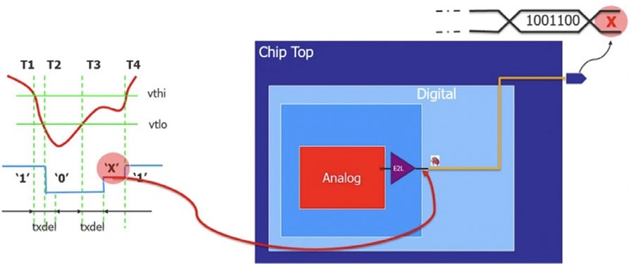
RVN! 26 Banner revised (800 x 100 px) (600 x 100 px)

Intel Architecture Day – Part 1: CPUs

Intel Architecture Day – Part 1: CPUs
by Tom Dillinger on 09-01-2021 at 6:00 am

performance core

Introduction

The optimization of computing throughput, data security, power efficiency, and total cost of ownership is an effort that involves managing interdependencies between silicon and packaging technologies, architecture, and software.  We often tend to focus on the technology, yet the architecture and software utilities have as important a contribution to competitive product positioning, if not more so.  Intel recently held their annual “Architecture Day”, providing an extensive set of presentations on their product roadmap.

The breadth of topics was vast, encompassing:

  • (client and data center) x86 CPUs
  • (discrete and integrated) GPUs, from enthusiast and gaming support to high performance AI-centric workloads
  • Interface Processing Units (IPUs), to optimize cloud service provider efficiency
  • operating system features for managing computing threads in a multi-core complex
  • open industry standards for software development application interfaces, focused on the integration of CPU and accelerator devices

This article will attempt to summarize key features of the upcoming CPU releases; a subsequent article will summarize the balance of the presentations.

 “Performance” and “Efficient” x86 Cores

Intel introduced two new x86 core implementations – an “efficient” (e-core) and a performance-centric (p-core) offering.

The design considerations for the e-core included:

  • cache pre-fetch strategy
  • instruction cache size, and data cache size
  • L2$ (shared memory) architecture across cores
  • branch prediction efficiency, branch target buffer entries
  • instruction prefetch bandwidth, instruction retire bandwidth
  • x86 complex instruction micro-op decode and reuse strategy
  • out-of-order instruction dependency management resources (e.g., allocate/rename register space)
  • configuration of various execution units, and address generation load/store units

To maximize the power efficiency of the e-core, a wide (dynamic) supply voltage range is supported.

In the figure above, note the units associated with the x86 instructions using vector-based operands, to improve performance of the “dot-product plus accumulate” calculations inherent to deep learning software applications:

  • Vector Neural Network Instructions (VNNI, providing int8 calculations)
  • Advanced Vector Extensions (AVX-512, for fp16/fp32 calculations)

These instruction extensions accelerate neural network throughput.  Active research is underway to determine the optimal data format(s) for neural network inference (with high accuracy), specifically the quantization of larger data types to smaller, more efficient operations – e.g., int4, int8, bfloat16.  (The p-core adds another extension to further address machine learning application performance.)

An indication of the e-core performance measures is shown below, with comparisons to the previous generation “Skylake” core architecture – one core executing one thread on the left, and four e-cores running four threads on the right:

Whereas the efficient-core is a highly scalable microarchitecture focusing on multi-core performance per watt in a small footprint, the performance-core focuses on performance, low-latency and multi-threaded performance, with additional AI acceleration.

For example, the p-core buffers for OOO instruction reordering management and for data load/store operations are deeper.

As mentioned above, applications are selecting a more diverse set of data formats – the p-core also adds fp16 operation support.

Perhaps the most noteworthy addition to the p-core is the Advanced Matrix Extension instruction set.  Whereas vector-based data serve as operands for AVX instructions, the AMX operations work on two-dimensional datasets.

Silicon “tiles” representing 2D register files are integrated with “TMUL” engines providing the matrix operations, as illustrated above.

The addition of AMX functionality is an indication of the diversity of AI workloads.  The largest of deep learning neural networks utilize GPU-based hardware for both training and (batch > 1) inference.  Yet, there are many AI applications where a relatively shallow network (often with batch = 1) is utilized – and, as mentioned earlier, the use of smaller data types for inference may provide sufficient accuracy, with better power/performance efficiency.  It will be very interesting to see how a general purpose CPU with AMX extensions competes with GPUs (or other specialized hardware accelerators) for ML applications.

Thread Director

A key performance optimization in any computer architecture is the scheduling of program execution threads by the operating system onto the processing resources available.

One specific tradeoff is the allocation of a new thread to a core currently executing an existing thread.  “Hyperthread-enabled” cores present two logical (virtual) processors to the O/S scheduler.  Dual architectural state is provided in the core, with a single execution pipeline.  Register, code return stack buffers, etc. are duplicated to support the two threads, at a small cost in silicon area, while subsets of other resources are statically allocated to the threads.  Caches are shared.  If execution of one thread is stalled, the other is enabled.  The cache memory offers some benefit to the two threads, as shared code libraries may be common between threads of the same process.

Another option is to distribute thread execution across separate (symmetric) cores on the CPU until all cores are busy, before invoking hyperthreading.

A combination of p-cores and e-cores in the same CPU (otherwise known as a “big/little” architecture) introduces asymmetry into the O/S scheduler algorithm.  The simplest approach would be to distinguish threads based on foreground (performance) and background (efficiency) processes – e.g., using “static” rules for scheduling.  For the upcoming CPUs with both p- and e-cores, Intel has integrated additional power/performance monitoring circuitry to provide the O/S scheduler with “hints” on the optimum core assignment – i.e., a runtime-based scheduling approach.  An illustration of Intel’s Thread Director is shown below.

Additionally, based on thread priority, an executing thread could transition between a p-core and e-core.  Also, threads may be “parked” or “unparked”.

P-cores support hyperthreading, whereas e-cores execute a single thread.

Intel has collaborated with Microsoft to incorporate Thread Director support in the upcoming Windows-11 O/S release.  (Windows-10 will still support p- and e-core CPUs, without the real-time telemetry-based scheduler allocation.  At the Architecture Day, no mention was made of the status of Thread Director support for other operating systems.)

Alder Lake

The first release of a client CPU with the new p- and c-cores will be Alder Lake, expected to be formally announced at the Intel InnovatiON event in October.

In addition to the new cores, Alder Lake incorporates PCIe Gen 5 and DDR5 memory interfaces.  The Alder Lake product family will span a range of target markets, from desktop (125W) to mobile to ultra-mobile (9W), with an integrated GPU core (I7 node).

Sapphire Rapids

The first data center part with the new p-core will be Sapphire Rapids, to be formally announced in 1Q2022 (Intel7 node).

The physical implementation of Sapphire Rapids incorporates “tiles” (also known as “chiplets”), which utilize the unique Intel EMIB bridge silicon for adjacent tile-to-tile dense interconnectivity.

Note that Sapphire Rapids also integrates the Compute Express Link (CXL1.1) industry-standard protocol, to provide a cache-coherent implementation of (heterogeneous) CPU-to-memory, CPU-to-I/O, and CPU-to-device (accelerator) architectures.  (For more information, please refer to:  www.computeexpresslink.org.)

The memory space is unified across devices – a CPU host manages the cache memory coherency.  An I/O device typically utilizes a DMA memory transfer to/from system memory, an un-cached architectural model.  With CXL, I/O and accelerator devices enable some/all of their associated memory as part of the unified (cache-coherent) memory space.  The electrical and physical interface is based on PCIe.  PCIe Gen 5 defines auto-negotiation methods for PCIe and CXL protocols between the host and connected devices.

Another unique feature of Sapphire Rapids is the application of HBM2 memory stacks integrated into the package, as depicted below.

The intent is to provide memory “tiering” – the HBM2 stacks could serve as part of the “flat” memory space, or as caches to external system memory.

Summary

Intel recently described several new products based on p-core and e-core x86 architectural updates, to be shipped in the next few calendar quarters – Alder Lake (client) and Sapphire Rapids (data center).  A new Advanced Matrix Extension (AMX) microarchitecture offers a unique opportunity to accelerate ML workloads, fitting a gap in the power/performance envelope between AVX instructions and dedicated GPU/accelerator hardware.  The execution of multiples threads on asymmetric cores will benefit from the real-time interaction between the CPU and the (Windows-11) O/S scheduler.

These products also support new PCIe Gen5, DDR5, and the CXL1.1 protocol for unified memory space management across devices.

As mentioned in the Introduction, optimization of systems design is based on tradeoffs in process technology, architecture, and software.  The announcements at Intel Architecture Day provide an excellent foundation for current and future product roadmaps, through successive technology generations.

-chipguy


AMS IC Designers need Full Tool Flows

AMS IC Designers need Full Tool Flows
by Daniel Payne on 08-31-2021 at 10:00 am

AMS tool flow min

Digital IC design gets a lot of attention, because all of our modern devices primarily use digital logic, but in reality whenever you have a sensor like a camera,  accelerometer, gyroscope or any radio like Bluetooth, WiFi or NFC, then you’re really in the realm of analog, and that’s where mixed-signal  IC design comes into play.  Siemens EDA has put together an analog/mixed-signal IC design tool flow that looks pretty capable, so I got an update by downloading their latest White Paper on the topic. I did work at Mentor Graphics back in 2003, but a lot has changed over the past 18 years.

Let’s first look at the big picture of the tool flow, split into the Analog (Blue), Digital (Green) and Mixed-Signal (Grey) domains.

AMS Tool Flow

This AMS tool flow supports process node PDKs spanning from 0.5um, all of the way down to 22nm at the following foundries:

Open Access is used as the open reference database for IC design, allowing interoperability between EDA vendors, foundries and fabs. You can even use your favorite data management tool, like: IC Manage, Cliosoft and SubVersion (SVN).

Schematic Capture

On the front-end, engineers use the S-Edit tool, which came from Tanner EDA in a 2015 acquisition, where you can do transistor-level design, create SPICE netlists, edit Verilog, work with Verilog-A, use Verilog-AMS, or even code VHDL.

S-Edit

Circuit Simulation

Mentor acquired Berkeley Design Automation back in 2014 and has continued to enhance the Analog FastSPICE (AFS) circuit simulator which is used for analog, RF, mixed-signal and even custom digital circuits. There’s tight integration between S-Edit, AFS and the waveform viewer called EZwave. With Tanner Designer you can do analog verification management, so engineers have a dashboard to see all of their specifications as passing or failing.

EZWave

Mixed-signal Verification

To verify both digital and analog portions of an IC design you need to  simulate both realms together, and that’s where the AFS circuit simulator for analog plus Questa simulator for digital come together, and the combination is called Symphony.

Setting up a mixed-signal simulation is done with S-Edit, and each cell instance has a view for the desired abstraction: Schematic, Verilog-A, Verilog, VHDL, SPICE. At the interface between analog and digital ports the Symphony tool automatically inserts a Boundary Element to convert signals properly. Both analog and digital signals are displayed in Symphony, so debugging the AMS interfaces during verification is quicker.

Mixed-signal waveforms

Custom IC Layout

The companion to S-Edit for layout is dubbed L-Edit, and it uses OpenAccess for interoperability, while also supporting PCells for parameterized layout generation. Save time by using Schematic Driven Layout (SDL) along with PCells. Decrease layout verification iterations by using the L-Edit IC Rule-Aware Layout so that you can visually see design rules appear while editing, and it will enforce correct layout.

IC Rule-Aware Layout

Digital Implementation

Physical synthesis comes from the Oasys-RTL tool, acquired back in 2013, then the placement and routing task is completed with the Nitro tool.  Both tools are launched from the GUI in L-Edit, or you can use command line control if preferred. The complex P&R steps are guided by the Nitro reference flow:

Nitro reference flow

Physical Verification

Siemens EDA is quite famous for it’s leading-edge Calibre tool, and it has several parts called from L-Edit:

  • Calibre nmDRC – IC layout design rule checking
  • Calibre nmLVS – IC layout versus schematic checking
  • Calibre xRC – IC layout extraction for analysis in a circuit simulator like AFS
  • Calibre RVE – Results Viewing Environment, for faster layout debug
  • Calibre RealTime – interactive DRC checking, prevention approach

    DRC Results

Summary

AMS design is harder than just Digital design, so having the right tools and a complete flow of tools will certainly make the task less error-prone, and get done more quickly. Siemens EDA has built up a lot of AMS tool flow experience in the last decades by tightly integrating their own point tools together, while at the same time adopting standards like OpenAccess to ensure interoperability. Whether you adopt an analog on top, or digital on top approach to AMS IC design, both approaches are supported in the Siemens EDA tool flow.

It’s also a healthy sign that so many of the EDA point tool acquisitions have worked out so well over the years in this AMS too flow. Read the complete 10 page White Paper here.

Related Blogs


Smoothing the Path to NoC Adoption

Smoothing the Path to NoC Adoption
by Bernard Murphy on 08-31-2021 at 6:00 am

Arteris customers min 1

We’re creatures of habit. As technologists, we want to move fast and break things, but only on our terms. Everything else should remain the same or improve with minimum disruption. No fair breaking the way we do our jobs as we plot a path to greatness. This is irrational, of course. Real progress often demands essential changes where we’d rather not see them. Still, we all do it, even if unintentionally. Which becomes apparent when evaluating an IP block or tool change in our design flows, herein considering NoC interconnects as an alternative to crossbars. I talked to Matt Mangan and Kurt Shuler (respective FAE manager and VP marketing at Arteris IP) about their experiences in smoothing the path to NoC adoption.

How not to benchmark a NoC

You’re a strong design team with a successful first-generation product in production. Now the product plan calls for premium versions requiring x2 and x4 instantiations of some pretty bulky subsystems. You know you struggled to close timing and meet cost on the first generation. Congestion and area will be even worse on these new versions. You’ve heard good things about NoC interconnect, so you launch an evaluation.

What’s the first obvious thing to do? Start with the production RTL and simply replace each crossbar in the interconnect hierarchy with a NoC. Which gives you a cascading structure of NoCs mirroring the structure of crossbars you had. NoCs are supposed to be more area and congestion efficient, so you should see this in the trial, right?

Wrong. Designing a NoC this way immediately throws away its area and congestion advantages. It might even look worse than the crossbar implementation. Matt puts it this way: when you design with crossbars, you build your design around the interconnect. When you design with a NoC, you build the NoC around the design. In simple terms, you floorplan the IPs the way you want them to layout, then you let the NoC flow through the gaps between those IPs. There will be some iterations to expand room for NoC routes here and there, but the intent remains. Therefore, to get a meaningful measure of NoC impact on the design, you should rip out all the crossbar structures and build the NoC flat.

Matt mentioned one customer working on a mid-sized automotive application. A back-of-the-envelope calculation estimated that a crossbar interconnect would cost about 10 square millimeters of area, clearly unreasonable. When they prototyped a flat NoC implementation, they got down to 5% of the size. Why the huge difference? The internal structure of the flat NoC dispenses with a vast number of redundant switches, wires and control.

I don’t need a NoC. My design is tiny

Sometimes it doesn’t feel sensible to even consider a NoC. Think of a Bluetooth toothbrush. The SoC and the interconnect will be about as small as you can imagine. Unchallenged by congestion or area. But this is a battery-operated, consumer device. It’s very important to run a toothbrush for multiple days between recharges. Anything a design team could do to further reduce power would be a win.

In a low-power design, you’ll power-gate and clock-gate IPs everywhere you possibly can, even down inside the IPs where possible. But you don’t have that level of control on a crossbar. Either it’s all on or it’s all off. However, a NoC can be gated internally, unlike a crossbar. In fact, NoCs can provide very fine-grained control over dynamic and static power.

This power management is completely configurable through the Arteris IP NoC generator and just as intelligently managed as in power management for endpoint IP. Waking up when needed, powering down when not needed. Effectively off 99% of the time, a real competitive advantage over a traditional interconnect.  Arteris IP had such a customer who used their NoC for precisely this reason.

My design is a monster. I must have a custom network

Then again, maybe your design is so massive and latency-sensitive that the only way you can see making it work is through hand-crafted communication. AI training accelerators for hyperscale datacenters are a good example. Often these are built as arrays of processing elements, but not uniform arrays because you leave holes for caches, scratch memories and other goodies. And you want to tweak network logic to minimize every picosecond of latency. Also, adding special networking for direct broadcast and aggregation, bypassing the standard network.

AI teams all over the world are building such accelerators to gain competitive advantage. Arteris IP has been working with leaders in the field for many years and has been able to evolve what they offer in step with those evolving design needs. Now, AI designers can fine-tune their NoC networks without having to hand-craft RTL. All the advantages of customization while retaining the advantages of a generator solution.

NoCs have broader appeal than you may realize

All sounds good, but who is really invested in these NoCs? The graphic at the head of this article will give you some idea. You can learn more about Arteris IP NoC solutions HERE.

Also Read:

The Zen of Auto Safety – a Path to Enlightenment

IP-XACT Resurgence, Design Enterprise Catching Up

Architecture Wrinkles in Automotive AI: Unique Needs


Webinar – Why Keeping Track of IP in the Enterprise Really Matters

Webinar – Why Keeping Track of IP in the Enterprise Really Matters
by Mike Gianfagna on 08-30-2021 at 10:00 am

Webinar – Why Keeping Track of IP in the Enterprise Really Matters

Everyone knows IP is an important asset for the enterprise. You spend a lot of money on IP licenses. You try to keep track of who bought what as buying the same thing twice is painful. You wonder if you have the latest version of an IP, especially if it’s part of mission-critical functionality. If you’re a good corporate citizen, you want to let others know if you find and fix a problem with a piece of IP, no matter where it came from. All these items will sound familiar to most. The real question is, do you have a complete view of the process and a complete view of the impact of doing it right? After all, IP management isn’t part of front-line chip design, so why do it? All these questions get answered in a recent Cliosoft webinar. Read on to understand why keeping track of IP in the enterprise really matters.

Karim Khalfan

A replay link is coming, but first a bit about the presenter. Karim Khalfan is the vice president of application engineering at Cliosoft. He’s been at Cliosoft for over 18 years, so he knows a bit about their products and the impact of design data management. I’ve attended other presentations from Karim and I can tell you he has a gift to both make any topic interesting and make it relevant for you. This webinar lives up to these comments. Some may think topics like BOM management and IP traceability are boring. Karim takes you through a real design scenario in the webinar, using a real design team’s personas. You will get the full impact of how important the topic is and why keeping track of IP in the enterprise really matters.

The webinar focuses primarily on Cliosoft Hub, a product that facilitates cataloging of semiconductor IP and efficient collaboration across multi-site teams. The use of Cliosoft SOS is also discussed and how the tools work together. SOS is Cliosoft’s hardware design data management product. Karim begins with an overview of BOM management, what it is, how it impacts the design and what tools are available to track and visualize the BOM. IP traceability and the associated knowledgebase are discussed next. I can tell you there are many more dimensions to this piece than you may be aware of. Watch the webinar to find out more. Key industry certifications of the product and document tracking are also covered by Karim.

The rest of the webinar takes you through a real-life design scenario with various personas that play different roles in the design process. Karim takes you through the modification of a piece of IP, the check-out and check-in process, as well as the steps to publish the new version and how that is propagated through the design community. During the demo you will understand how Cliosoft HUB and SOS interact and how these tools interface with other parts of the design flow, such as Jira.

A snippet of the demo

Watching the demo, you will get a real sense of how the Cliosoft tools are used in a real design project. Ease of use, impact analysis and how to propagate the right information to the right people are all clearly explained and demonstrated. If you use internally developed or third-party IP in your designs (and who doesn’t) you will want to watch this webinar to fully understand what capabilities exist to make your life easier and less stressful. A critical part of any tool like this is understanding how it fits in your workflow without getting in the way. The webinar will help with that, too. If you’d like to understand why keeping track of IP in the enterprise really matters, you can check out this webinar here. I highly recommend it.

Also read:

CEO Interview: Srinath Anantharaman of Cliosoft

Close the Year with Cliosoft – eBooks, Videos and a Fun Holiday Contest

The History and Physics of Cliosoft’s Academic Program!


NetApp’s ONTAP Enables Engineering Productivity Boost

NetApp’s ONTAP Enables Engineering Productivity Boost
by Kalar Rajendiran on 08-30-2021 at 6:00 am

What if you could Table

One of the few things that remain constant in the engineering world is the desire for higher productivity. Innovation happens when engineers are designing something and creative ideas crop up when they are reviewing and analyzing the results. In between these fun steps, engineers have to deal with the necessary evil of creating workspaces, check-ins/check-outs, compiles, builds, releases, etc. These steps fall into the category of overhead time from an engineering productivity perspective.

What if you could…

How would you reimagine your EDA and SW development workflows if your design DATA were Agile?

I recently had a conversation with Scott Jacobson, EDA Solution Strategist and Michael Johnson, EDA Solution Architect, both from NetApp. I learned about some powerful capabilities of NetApp’s ONTAP Data Management Operating System that may very well be a secret to many. These capabilities, when leveraged can yield a productivity gain of 10% and above.  Refer to a testimony from a “Top 3 Fabless Semiconductor Company.”

“It’s an incredibly powerful tool – instead of messing with builds / build artifacts / minor trees, where some builds have to run overnight, and messing with environments can take an hour or more a day, now the developers just take 5-10 minutes to create a clone. Now they can focus on what they were hired to do – develop chips…” —VP, Engineering

The purpose of this blog is to bring awareness of ONTAP’s powerful capabilities to a broader base, so more could increase their engineering productivity. There will be a follow-on blog that will be structured like a playbook or application notes detailing specific steps.

Changing Semiconductor Economics

The cost associated with 7nm, 5nm and now 3nm designs are growing exponentially due to ever increasing design complexity, transistor density and FinFET data growth.  Development costs are dominated by the cost of engineering (people), EDA licenses and infrastructure over time.  Shorten development time and we lower costs. Improve people, license, and infrastructure utilization and we lower costs.  To materially impact the economics of chip development, we need to improve the time and the resources utilization.

Where are your innovation and productivity speed bumps?

Is innovation hampered by the time spent managing ever growing backend data sets?

Are your engineers

    • Waiting on Daily or Weekly code checkouts and builds that take hours?
    • Burning precious time tracking down regression bugs and backing out bad code commits?
    • Spending time fixing or rebuilding corrupted workspaces?
    • Being paranoid that a large backend design flow might break while trying to test a new idea or option?

What if you could transform all the above overhead into faster design interactions, quicker debugs, rapid innovations, lower development costs and improved development velocity?

NetApp’s ONTAP Data Management Operating System makes Data Agile

For over 25 years, NetApp’s ONTAP data management operating system has been helping semiconductors companies successfully develop chips.  Most designers know about the .snapshot directory as the read-only hourly, nightly or weekly backup or “crap I need to recover a file”, directory that has saved you from potential disaster.

But many may not know that same Snapshot (or instant point in time READ-ONLY volume copy) can be created on-demand with a single API call with a snapshot name of their choice – say snapshot name of “chip-projectA-p4ID_1234”.  The snapshot is an instant copy of the entire data volume.

Many are not aware that they could make another single API call and create an almost instant new READ/WRITE-able copy of an entire volume of data regardless of size.  NetApp’s ONTAP operating system makes replicating massive amounts of design data as fast as the video graphics in Forte Night.  ONTAP is like a data accelerator card for your development environment.

Instant Data Replication Regardless of Data Size

The ONTAP Data Management Operating System through its Snapshot and FlexClone capabilities can instantly replicate data, no matter how large the data size. It works in a way similar to 2D/3D Graphics cards off-loading CPU intensive graphics operations to a dedicated graphics rendering engine. A single NetApp RESTful API call can make a nearly instant point in time read-only copy (Snapshot) of a volume of data regardless of the size. Another single NetApp API call can make a nearly instant read/writeable storage efficient copy of a volume of data of arbitrary size. Call it data management completely off-loaded from the compute server – Agile Data Accelerated.

How would you revamp your EDA and SW development workflows with such a powerful data management tool that works for both on-prem and in the cloud?

The True Impact of Data Agility in a Chip Design Flow

Here are a couple of real-life examples of productivity gains by NetApp’s customers.

A customer who integrated Snapshots and FlexClone API calls into their design process saw Code Checkout times of roughly 1 hour followed by front-end build times of 2 hours reduced to less than two minutes.  That is roughly a 3-hour faster time to productivity.

Another customer who has been using Snapshots and FlexClone in their front-end design and verification workflow has seen a reduction of Perforce code checkouts and VCS build times from around 60 minutes down to under 5 minutes.  Now multiply that time savings by the number of developers in your organization who rely on fast code checkouts and builds and you get an idea of the magnitude of impact on developer productivity.

But the benefit it not limited to just engineering productivity increase.  The above customer also saw a dramatic reduction in their P4/ICManage server load because of developers Cloning vs Checking out. This customer also saw a reduction in license, LSF compute and storage because the clone workspaces were already built.

The following graphic quantifies the productivity gain for a team  in monetary terms for an example scenario of 500 developers. The data agility enabled by ONTAP can deliver a 10% productivity improvement as a conservative estimate. That is the equivalent of 50 additional engineers working on your designs.


Ready to transform your engineering environment?

If you are already using NetApp for your chip or software development, you already have what you need to get started.  If you’re not currently using NetApp, you may want to explore leveraging it, going forward. The next blog will get into the technical details and how to get started on the path to increasing your engineering productivity.


GM Fires First 5G Shot

GM Fires First 5G Shot
by Roger C. Lanctot on 08-29-2021 at 10:00 am

GM Fires First 5G Shot

Connecting cars remains one of the most unnatural acts in the world of IoT. “Connected Car” headlines might make you think otherwise, but the reality is that precious few cars on the road today are connected with a live, provisioned and functioning wireless connection. That being said, General Motors claims 16M of those cars on its own OnStar network making the company the de facto leader in car connectivity.

Noting GM’s leadership is significant in a world where the one-time ruler of the automotive industry (now the sixth largest ranked by global vehicle sales) has spent decades exiting markets, laying off workers, and closing factories. All of that downsizing has failed to diminish GM’s technology leadership emanating like a beacon from its Warren, Mich., Tech Center and development operations in Israel, Canada, Georgia, Texas, Silicon Valley, and China.

When GM makes a technology announcement it is a signal to the global automotive industry that The General can still call the tune. That’s precisely what GM did this week in announcing its plans to launch 5G connectivity in select vehicle models beginning with model year 2024. The announcement follows, by one year, the company’s announcement of its plans to launch 5G in select models in China in model year 2022.

GM isn’t the only car company bringing 5G connectivity to vehicles, It is the first, though, outside of China, to lay its 5G cards on the table. The current 5G announcement is reminiscent of GM’s launch of LTE-enabled OnStar connectivity in all of its cars (in the U.S.) beginning in 2014.

To this day, though, car companies including GM struggle to define a message around vehicle connectivity that is compelling to consumers. At its launch more than 25 years ago, OnStar was able to leverage the novelty of vehicle connectivity and the fear factor to sell the solution: If you are ever in a crash, OnStar will ensure that help is on the way with its built in automatic crash notification (ACN). GM has notably revived those commercial messages in recent weeks.

The onset of smartphones more than 10 years ago introduced a false sense of security for most drivers, dissolving the fear factor. Auto makers have struggled since to define a new car connectivity message sufficient to convince customers to part with $10-$20/month or more for a subscription.

When GM introduced LTE connectivity and inaugurated its current partnership with AT&T it offered in-vehicle Wi-Fi along with the ability to add your GM connected vehicle to your AT&T wireless plan. Both offers were intriguing enough to attract at least some interest – but not enough to solve the connectivity customer retention challenge.

The subscription drive by car makers such as GM reflects an enduring desire to “monetize” the vehicle connection. GM and its rivals offer elaborate subscription packages including Wi-Fi, access to on-board streaming (instead of streaming via a connected smartphone), software updates, and search. None of these offers have generated much traction – though consumer awareness and interest is slowly growing.

Only one company has succeeded in insinuating a seamless connectivity into the daily car ownership experience: Tesla. Tesla owners drive vehicles that operate almost like sentient beings – anticipating troubles ahead and interacting with their drivers. The wireless connection is either included in the price of the vehicle or the buyer is required to pay a nominal $10/month for Internet access – which supports a hybrid navigation experience.

Wireless connectivity is not a big part of the Tesla experience unless you consider the heartbeat of monthly software updates (most often handled via Wi-Fi actually), and access to Internet search important. Of course, you can also stream Netflix in your Tesla while you’re charging – but that isn’t a daily scenario. Tesla isn’t pushing a connectivity subscription beyond the $10 a month, though it has proposed a $199/month self-driving subscription.

The onset of 5G does promise a different connected car experience including higher speed communications, lower latency and direct communications with other 5G-equipped cars (mainly for collision avoidance applications), enhanced vehicle location technology, and a more reliable connection. Most important of all, though, is that the 5G connection at launch will be backward compatible to LTE.

The transition to 5G will not leave LTE-equipped cars without connectivity. That being said, 5G arrives as 2G and 3G networks in the U.S. and, in a few years, in Europe, are being decommissioned. This, too, will accelerate 5G adoption.

It is no exaggeration to say that both the wireless industry and the automobile industry were waiting eagerly for GM’s announcement. Connecting cars is an expensive business and one that, these days, is fraught with cybersecurity concerns. It’s just hard for an automotive engineer to get excited about connecting cars when customers are ambivalent and the return on investment is unclear.

Add to these concerns regulatory uncertainty regarding the use of the 5.9Ghz band and the result was an entire industry frozen in amber – unwilling to commit to the adoption of next generation wireless connectivity. GM’s announcement was the essential starting gun – the ice breaker – that will spur competitors to cop to their own 5G plans.

The announcement may also help return some respectability to the business of connecting cars. AT&T is GM’s anointed connectivity partner. Even if car makers are still struggling to define the connected car killer app, there is no chance AT&T would risk suffering the ignominy of losing GM to a competitor such as T-Mobile or Verizon.

To drive home the importance of the AT&T-GM relationship, GM’s press release notes:  “Since the launch of 4G LTE in 2014, GM owners have used more than 171M gigabytes of data across its brands, which is equivalent to nearly 5.7B hours of music streamed or more than 716M hours of streaming video.”

Curiously, GM did not highlight in its announcement how many emergency response notifications it has received historically or in the past year – including lives saved, stolen vehicles recovered, and drivers assisted. This is a clear disconnect that reflects GM’s struggle to come to terms with the challenges of connected car messaging.

In fact, GM is at the heart of an important industry inflection point. Soon, vehicles around the world will require connectivity to fulfill safety mandates designed to reduce or avoid vehicle collisions. GM’s own Super Cruise hands-free driving system requires an OnStar subscription to operate.

In the near future multiple in-vehicle systems from navigation to intelligent speed assistants and, of course, software updates will require vehicle connectivity. All cars will eventually come with a subscription in addition to the sticker price. It’s either reassuring or alarming to see that GM is struggling to come to terms with this reality. Presumably the marketing minds at GM have decided that the time isn’t quite right to highlight the reality of the OnStar subscription and its relevance to vehicle safety. Wi-Fi and streaming media access are seen as safer 5G talking points for now.

GM’s announcement will help to clear the fog of corporate ennui enveloping 5G car connectivity. The message is clear from The General that 5G cars are on their way – and GM intends to lead the evolution. Competing car makers can be expected to follow swiftly behind GM with their own announcements.

It comes down to a simple proposition. In a rapidly evolving 5G world – where 5G networks are rolling out globally faster than any previous network topology – no auto maker will want to be caught selling LTE cars against 5G-equipped cars. The 5G car won’t be merely a connected car. It will be an intelligent car – and GM wants to have the smartest cars on the road.


Accelerating Exhaustive and Complete Verification of RISC-V Processors

Accelerating Exhaustive and Complete Verification of RISC-V Processors
by admin on 08-29-2021 at 6:00 am

FIG 1 spec bug

As processor architecture and design development becomes completely liberated with open-source RISC-V instruction set architecture (ISA), the race to get RISC-V silicon in our hands has increased massively. We have no doubt that in next 5 years, we will see RISC-V based laptops and desktops in the market. But would these processors be of high quality? Would any one of them have a glitch like the famous Intel FDIV bug from the era of mid 90s? Have we learnt what it takes to robustly verify these processors for safety-critical domains, security and functionality?

In this article, we would like to explore these questions from the perspective of open-source RISC-V architecture and will take a look at verification trends and what makes processor verification hard and how it can be made easier with the use of formal methods in particular using the fully automated vendor-neutral formal formalISA® app from Axiomise in combination with the JasperGold® Formal Verification Platform from Cadence. We also discuss a new automated debug, analysis and reporting solution (i-RADARTM) from Axiomise that allows accelerated debug and reporting.

Why is processor verification hard?

Designers are turning to the RISC-V ISA to create many different power/performance-optimized processor architectures for a wide range of devices, from mobile and IoT-Edge all the way to high-end servers. However, each different implementation must execute every single instruction in the ISA with complete functional consistency. This consistent functionality must be fully verified for the wide range of unknown datasets the devices could encounter, which is challenging for traditional verification methods to achieve.

Additionally, pipelined architectures with complex multi-threading and out-of-order execution pose significant challenges for verification. Common verification bugs not easily caught in simulation are due to concurrency, stalling, interrupts, race-conditions, arbitration, and memory ordering.  Debug introduces a significant additional challenge and ensuring it is not creating any security leaks poses another headache for designers.

What is the industry doing about it?

Simulation-based verification using UVM relies heavily on stimulus randomization to kick-off verification and uses functional coverage to sign-off.  With the complexity and size of the processors, it is not easy to model stimulus that can reach the deep wilderness of micro-architectural state-machine interactions that would be capable of exposing all the bugs in the processor. Functional coverage relies heavily on the very same stimulus and randomization that means your sign-off capabilities are limited – never mind that none of this is exhaustive.  Bringing up the UVM infrastructure in terms of human effort to the point that it can yield acceptable functional coverage yield is legendary. Harry Foster’s Wilson research report points out that processor design houses hire 5 verification engineers for every designer, and yet in the very same report where simulation is clearly shown to be the king, points out that 68% of ASICs and 83% of FPGAs fail in their first spin.

So, while it is totally understandable that most of the industry understands simulation-based verification and it is always easy to plod along with what you know best, the complexity of verification challenges and inadequacies of UVM-based verification has forced the industry to adopt formal – and the owners of the established ISAs like Arm and Intel have led the way. These industry leaders knew that consistent behavior of the ISA, across myriad implementation architectures, was vital for a software ecosystem to develop around the ISA. With no single entity responsible for its integrity, ISA verification is even more important for companies investing their resources in RISC-V. Furthermore, if history is anything to learn from, then the Intel FDIV and the more recent family of security flaws – offspring of meltdown and spectre should be an eye opener. Your silicon must work the very first time you bring it up and must always work – many years later – as expected without locking up, and without getting exposed to hackers.

Formal verification: The only gateway for providing exhaustive guarantees

For industry to achieve high-quality verification at reduced cost – formal verification is the only way forward. Writing formal properties takes a fraction of time compared to instrumenting UVM testbenches. Running these formal properties takes even less time. In the last two years, it has repeatedly been shown how Axiomise formal verification solutions prove 27,000+ properties exhaustively on processors such as cv32e40p, ibex, 0riscy and now more recently WARP-V family of processors with six stage in-order pipelines within a few hours.

Yes, there is a human effort needed to code formal properties and it does need experience to know what to code, and how to code the properties efficiently. This is exactly why Axiomise teach formal verification courses – both online self-paced as well as instructor-led.

Axiomise partners with Cadence to offer these courses for customers using the industry-leading JasperGold formal verification platform. However, when there aren’t the resources to learn formal, and deliver high-quality formally verified designs to customers in the time required, then one can buy Axiomise off-the-shelf formal verification solution for RISC-V.

WARP-V Case Study

WARP-V is a brilliant design from Steve Hoover CEO, of  RedWood EDA to promote TL-Verilog – a new transactional flavour of Verilog designed to make designers efficient in bringing up designs with fewer bugs and ultimately build RTL correct-by-construction. The beauty of this infrastructure is the ease with which you can design multi-stage pipelined designs with the same canonical high-level TL Verilog model. In fact, we can also extract Verilog out of it and the extracted Verilog is still very much readable.

Formal verification of WARP-V

When Steve designed the WARP-V processor, there were numerous articles written to demonstrate these concepts including many on how Steve and Ákos Hadnagy formally verified the processor. Steve had used the open-source solution. When Steve announced that it was used to verify WARP-V everyone including me trusted that it would be bug-free.

WARP-V formal verification using  formalISA®

So, when Shivani Shah started the work with Axiomise on formally verifying the WARP-V processors using the Axiomise’s formalISA solution, we didn’t think at the time we will find any bugs. Why would we find bugs when they already used formal verification? Right?

So, it came to us as real surprise when we started to see property failures within a few minutes of integrating the WARP-V core in our app. The initial instinct was that our verification solution may have an issue, or in fact that the integration was not correct, and mapping files used to configure the app had discrepancy.

When  Shivani dug deeper and opened tickets and started to inquire with Steve, it turned out that the issues we found were indeed true design bugs. The initial set of these bugs were all down to how the semantics of branch instructions were interpreted by us in formalISA (in accordance with the RISC-V ISA spec) and how Steve’s design model and the open-source RISC-V formal test bench that happen to agree with each other were not in compliance with the architectural spec. It meant that the WARP-V processors would work as processors but will break the requirements posed by the RISC-V ISA.   You can most certainly not expect the software to work as the compiler would behave one way and the hardware another. We scheduled face-to-face meetings with Steve and Akos and both confirmed that these were design bugs.

When we asked Steve as to why they had these bugs in the first place, Steve remarked that at the time of the design he was not clear about some aspects of the specifications, and he relied on using the interpretation of the formal semantics of the open-source RISC-V formal. It is not surprising that Steve didn’t find the bugs himself, but what was surprising was that the formal model used by them had this bug especially as that model is also used by other designers building RISC-V processors.

So, a note of caution: If you’ve been using the same semantics of branch instructions in your core that the open-source formal solution does, chances are you have the same bug in your core!

When Shivani expanded her work and started adding M-extensions to our app, even more bugs were picked up. The full list can be found from our Github page.

Previous verification work carried out with formalISA®

We used our app before to verify other processors. In the RISC-V summit 2019, we outlined our verification methodology providing details of how we start the verification and how checks are modelled in formal. We provided results on verifying 0riscy, and ibex. Although both were small, embedded designs with 2-stage pipelines and 0riscy was already verified before and was in silicon when we started the verification, we found over 65 bugs including deadlocks. Ibex was a near clone of 0riscy. When its development forked out, we looked at it in the early stages and caught several corner-case bugs affecting numerous instructions.

In 2020, we worked with the OpenHW group to formally verify the cv32e40p core. We were able to verify nearly 27,000 properties including extensive coverage in a matter of hours. These results have been presented in the RISC-V summit, 2020 as well as in the webinar in March 2021. We caught several bugs including an inconsistency issue in the published RISC-V ISA specification.

Example of a specification bug caught by formalISA

Fig 1. Inconsistency bug caught by formalISA app.

In the published RISC-V ISA specification v2.2, on page 30 it requires the generation of illegal instruction exception for the shift instructions SLLI, SRLI and SRAI if imm[5] is not equal to 0. However, it is not possible for imm[5] to be non-zero if the instruction decoded is one of the SLLI, SRLI and SRAI as the specification provides the opcodes for these on page 104.

Scenario coverage

Conventional verification of microprocessors relies heavily on architectural testing using simulation. Functional coverage with simulation would test the interactions of different instruction inter-leaving however, the quality of results is limited to specific stimulus patterns. With our scenario coverage we auto-generate assertions and covers to examine a range of interesting scenarios targeting optimizations such as forwarding, pipelined instruction interleaving and the inter-play of stalls, interrupts, and debug.

How does it work?

By reading a user-defined specification from an Excel spreadsheet, the formalISA app will generate proofs of assertions and coverage properties along with waveforms to establish beyond doubt that those specification entries always hold in all reachable states. The figure below shows a user entry specifying that 4 cycles after reset a SUB instruction was issued twice followed by 1-cycle later an OR instruction followed by 1-cycle later an AND instruction. This entry triggers a range of coverage targets (asserts and covers) that are proven in the formal tool. The waveform below shows a scenario satisfying this entry showing forwarding.

Fig 2. Scenario coverage example

Architectural verification planning and status dashboard

The beauty of our solution using the formalISA app is that users can find bugs in RTL or specifications, build proofs and auto-generate the entire verification plan, status and coverage results with a single push-button. The plan and status is linked directly to the RISC-V specification published by the RISC-V international.

 Fig 3. Snippet of an example verification plan and status dashboard for WARP-V generated automatically from formalISA®

When using a tool such as Cadence JasperGold® we are also able to generate a rich coverage dashboard exploiting the capabilities of JasperGold.

Fig 4. Coverage metrics obtained within minutes from JasperGold® on cv32e40p

Intelligent Rapid Analysis Debug and Reporting i-RADARTM

When Shivani was finding bugs and we were root-causing them together, it was a significant effort even though we were using formal methods and one of the best formal verification debuggers JasperGold® Visualize. The challenge is that although JasperGold® is already quite cool in how it identifies a precise set of signals linked to the failure of the property in many cases the signal identified are too precise as they are linked to the proof core.

What we mean here is that if a certain bit of a signal for example bit [1:0] of the branch address was responsible for the failure it will show just that, and the user then has to follow the trace systematically which is all good but it takes time for anyone debugging to pull together a narrative of why something failed and understand why it is a bug before it can be sent to a designer.

Without the narrative just with the trace, the designers would often complain about not knowing what is being debugged. To overcome this problem, we designed a new intelligent debug solution in Axiomise called i-RADARTM. It stands for intelligent rapid analysis, debug and reporting which is now offered by Axiomise as a plugin-solution for JasperGold when you purchase the formalISA app.

If you use JasperGold and formalISA app, you will see a GUI button in JasperGold. When you click this button, the Axiomise intelligent analysis is performed on a failing property and a debug report along with VCD is generated for debug handoff to the designers. It means that no human effort needs to be made to debug, troubleshoot, build a report.

i-RADAR in action

Fig 5. i-RADARTM solution showing the failure of the BEQ instruction on WARP-V.

The waveform image that appears when the i-RADARTM is used with Cadence JasperGold®. The trace shows the failing property on BEQ instruction in WARP-V. The precise chain of causality is annotated in the debugger. The report explaining why it is a design bug is also printed in a file shown below.

——————————————————————————————-

formalISA generated cover report for the instruction beq

Generated on 2021-08-22 17:07:44 %

beq.fsdb, beq.vcd, and beq.shm written on disk

——————————————————————————————-

The waveform is for the RISC-V instruction: BEQ

BEQ was triggered for execution and commit (u_isa.beq_instr_trigger) in cycle: 23

Design computes the branch target address in cycle 23 = 32’h00000034

Formal model computes the branch target address in cycle 23 = 32’h00000030

The formal model computes target address in cycle 23 using the PC (32’h00000001) and the offset (32’h00000030)

The value computed by the design 32’h00000034 does not match with the value computed by the formal model 32’h00000030

——————————————————————————————-

Why Axiomise formal verification solution matters?

Axiomise has invested in building an architectural model of the RISC-V ISA with support for privileged instructions as well as regular ones. Having spent years verifying processors, the Axiomise team has distilled down key abstraction techniques in the formalISA® app and ensured that we get them reviewed independently as well as against different processors. Our partnership with Cadence enables us to validate and optimize the formalISA® app for JasperGold® users.  Axiomise built the industry’s first scenario-coverage based solution as part of the six-dimensional coverage solution. Our solution is the only solution in the market that works with all the formal verification tools, is push-button and has smart automation from running the first proofs to intelligent debug, to obtaining a comprehensive coverage using the six-dimensions.

For more information, please check out the links:

Conclusion

Designing a processor is one thing, bringing it up in FPGA and demonstrating example program runs is another; but ensuring that this processor is able to run in silicon correctly as expected without having any functional, safety and security flaws is a completely different challenge.

Building silicon with zero defects is not easy and it requires a concerted focussed effort in combining the best verification technologies together to focus on verification concerns not on the political milestones of individuals driving verification. Let’s not kid ourselves anymore – simulation-based verification using UVM will not enable you to verify the processors with high quality never mind nowhere close to being exhaustive. Well known processor design houses such as Intel, IBM, Arm, and AMD have published numerous papers over the last three decades showing how they have complemented and supplemented their verification efforts with formal methods. Formal methods are the only way of obtaining exhaustive verification results, and sign-off your silicon so everyone can sleep better. Using formal methods, we can prove the absence of bugs, bring up corner-case (one in a million chance) bugs in a few seconds, and use different coverage techniques to convince through proofs that when formal says it’s done you are truly done.

Axiomise RISC-V formal verification app formalISA® when used in conjunction with top-end formal verification tools such as JasperGold® from Cadence provide a complete solution reducing human costs in bringing up bespoke testbenches and provides an accelerated path to exhaustive sign-off. With the combined new debug solution, we can perform automated intelligent analysis for a debug handoff to designers shrinking debug time and costs.

Authors:
Ashish Darbari, Axiomise
Pete Hardee, Cadence Design Systems

Also Read

CEO Interview: Dr. Ashish Darbari of Axiomise

Life in a Formal Verification Lane

Why I made the world’s first on-demand formal verification course


Podcast EP35: Benefits of FPGA Based Prototyping

Podcast EP35: Benefits of FPGA Based Prototyping
by Daniel Nenni on 08-27-2021 at 10:00 am

Dan is joined by Ying Chen, VP of marketing & international sales at S2C. Dan and Ying explore the various uses and benefits of FPGA-based prototyping, including the different architectures available and cloud access.

Mr. Chen is a dynamic technologist with over 23 years of technical and business experiences in digital IC industry, including 20 years focused on the FPGA market. Prior to S2C, he was the head of APAC marketing at Lattice Semiconductor. Mr. Chen also held sales management and technical roles during his 15-year tenure at Altera in the U.S. and Taiwan.

Mr. Chen received his bachelor’s degrees in Electrical Engineering and Computer Science (EECS) and Materials Sciences &Engineering from University of California, Berkeley.

The views, thoughts, and opinions expressed in these podcasts belong solely to the speaker, and not to the speaker’s employer, organization, committee or any other group or individual.


CEO Interview: Veerbhan Kheterpal of Quadric.io

CEO Interview: Veerbhan Kheterpal of Quadric.io
by Daniel Nenni on 08-27-2021 at 6:00 am

veerbhan kheterpal

It was my pleasure to meet Veerbhan Kheterpal. Veerbhan has founded three technology companies and has full stack expertise spanning software to silicon across Edge & Datacenter applications. Currently, he is a CEO & co-founder of quadric.io, a company that has created a new processor architecture for high performance on-device computing.

Prior to quadric.io, Veerbhan was a technical co-founder of 21, Inc where he was focused on bringing power-efficient ASICs to the cryptocurrency space. Veerbhan served in various roles ranging from designing custom ASICs (3 production chips in 18 months), developing web scale blockchain backends & building consumer facing mobile apps. Prior to 21, Veerbhan co-founded Fabbrix, Inc, which was acquired by PDF Solutions. Fabbrix was focused on software that enabled design for manufacturability of complex Integrated Circuits. Veerbhan is an entrepreneur at heart and always looking for breakthroughs in technology, relationships and parenting.

What’s the backstory of quadric?
In 2016, we started building an agricultural robot that was going to transform first, vineyard management, and eventually, crop management of any kind — reducing costs, minimizing arduous tasks for humans, and maximizing crop returns. While this might seem like a lofty goal, I was working with two talented partners, and we had just built and shipped a very complicated technical product in the bitcoin computing space. With our combined technical backgrounds, and access to cutting edge technology, we had no doubt about our ability to build this first-of-its-kind robot that would transform the agriculture industry.

We had just one problem: we couldn’t make it work. I mean we made it work — we wrote code and developed software and designed and built hardware prototypes that functioned. But we soon came to realize these prototypes would never become the affordable, scaleable, commercially viable products we had envisioned.

Why not? In short, the existing technology platforms built with CPUs and GPUs simply didn’t support the compute performance and capacity that was required with the power footprint. This forced us to conduct a deeper inquiry into the power consumption of our software. This led us down a path of inventing a new processor architecture; one that generalizes the dataflow paradigm and delivers on a higher level of power efficiency for a wide range of algorithms in Machine Learning, Computer Vision, DSP, Graph Processing & Linear Algebra. 

What problem are you solving?
Quadric’s processor is built by developers for developers. Developers are creative beings. Just like we were attempting to get cutting edge algorithms to work on our robot, developers continue to push the envelope of algorithms in order to bring delightful experiences to everyday devices. Recent examples of these algorithms are driven by rapid research in AI models. Once they have developed their dream algorithm, they start pulling their hair out when trying to deploy it at scale. Existing computing solutions for deploying intensive workloads are either too power hungry (think GPGPUs) or too restrictive in capability (think AI chips/accelerators). Further, AI inferencing doesn’t run on its own, it is frequently accompanied by classical data processing steps which require the developers to include additional specialized hardware such as FPGAs/DSP chips. Besides the hardware complexity, this leads to additional software integration complexity. Quadric’s architecture makes it easy to ship high performance AI inference combined with classical data processing with a single software model. 

Further, quadric’s architecture is scalable which means that if a certain power/performance combination does not fit your application, just pick a different size of our hardware keeping the software the same.

How fast does on-device AI get deployed? What are the applications?
Over the past several years we have seen at scale AI inference deployments in the cloud. A few examples such as recommendation engines and voice assistants come to mind. However, cloud deployment of inference has its limitations primarily due to privacy or round trip latency reasons. Due to latency reasons, robotics, automotive, video game consoles & smart sensors have already deployed on-device compute solutions and are gaining volume with tremendous momentum.

Recently, we are seeing privacy driven requirements that need compute to move away from the cloud and be deployed on-device. Driven by privacy laws, the security industry is going through this transformation. This is driving the next generation of devices to include on-device inference capability.

If you step back and view AI as tomorrow’s “data driven” software as opposed to yesteryear’s “code driven” software, we are going to see a future with more than 80% of devices performing some sort of deep neural network in the next 5 years.

What about on-device training of machine learning models?
Great question. Training at the Edge or on-device training has been very difficult so far due to lack of specialized hardware and the diversity of processors at the Edge. As the next generation of devices gain specialized compute capabilities, it becomes feasible to perform limited amounts of training on the device itself. Now, the possibility of it alone doesn’t drive adoption – you need powerful drivers to move the market. We are seeing one such driver starting to affect this change where a limited set of customers are looking for on-device hardware capability that allows them to portion of the AI training algorithm on the device itself. This is different from solutions like homomorphic encryption that also attempt to preserve privacy.

To summarize, it’s still early days of “training at the edge” but the driving forces are assembling and multiple solutions are being proposed.

On-device inferencing market is super hot. How does quadric stand out?

Software and hardware scalability.

Most solutions in AI chip space are focused on accelerating layers and topologies that are well known today. However, this means the developer is locked into the family of DNN architectures of today. AI is changing fast and still taking large innovative leaps. Because Quadric’s hardware is general purpose, our software can scale to any data parallel workload. This gives developers the superpower to ship any new algorithm whether it is a new type of DNN layer or a domain transformation without limitations.

Further, a single instance of Quadric’s architecture can scale from 200 milliwatts to 20 watts. This gives us scalability across multiple applications and makes it worthwhile for large customers to adopt Quadric’s solution. Quadric’s solution is also designed to deliver cutting edge performance while providing this level of software and hardware scalability.

The industry is moving towards using multiple domain specific accelerators. How does Quadric fit in?
Quadric has taken a general purpose dataflow approach to the high performance computing problem. Our secret sauce is in the co-design of our instruction set and the accompanying compiler software that optimize for simultaneous compute and data movement. Most others are taking a DNN specific dataflow approach that quickly becomes obsolete as AI models evolve. The key is to acknowledge that the full system requires AI inferencing that is accompanied by custom data preprocessing or post processing algorithms. Due to its general purpose nature, Quadric’s architecture can replace multiple types of accelerators (DSP, Vision, AI) with a single one. This leads to a win for our customers on several axis:

  • 2x-3x Faster Software Integration
  • 2x-3x Faster Hardware Integration
  • 2x-5x Higher Performance/Watt
  • 2x-3x Lower Latency
  • 2x-3x Lower Cost

As an entrepreneur, what advice would you give someone founding a startup or thinking about starting one in the semi space?

The semiconductor space is relatively harder for startups. This requires the right mix of short term thinking while having an organic path to building a long term defensible moat. My advice to entrepreneurs is to think critically about the semiconductor product and their value proposition. Here some questions that you want to answer:

  • Am I creating enough short term value to be able to build my company while having a path to becoming a sizable enterprise? E.g. The biggest risk that investors perceive is the “defensible path to scaling beyond the first few design wins”. 
  • Is my product going to get easily commoditized after everyone realizes its value? Eg. First movers on bitcoin mining chips made profits which later disappeared due to intense competition that caught up quickly.
  • How fast can competition catch up? 
  • Do I have a defensible moat even if a better product comes along?

Another key feature of valuable semiconductor companies is that they are not hardware companies! You have to think about software as early as possible in the game. At Quadric, we built the software before we built the hardware. We also consistently invested more than 70% of R&D capital in software. This strategy has worked well for us.

Also Read:

CEO Interview: Pete Rodriguez of Silicon Catalyst

CEO Interview: Sivakumar P R of Maven Silicon

Ten Lessons Learned from Andy Grove


Side Channel Analysis at RTL. Innovation in Verification

Side Channel Analysis at RTL. Innovation in Verification
by Bernard Murphy on 08-26-2021 at 6:00 am

Innovation New

Roots of trust can’t prevent attacks through side-channels which monitor total power consumption or execution timing. Correcting weakness to such attacks requires pre-silicon vulnerability analysis. Paul Cunningham (GM, Verification at Cadence), Raúl Camposano (Silicon Catalyst, entrepreneur, former Synopsys CTO) and I continue our series on research ideas. As always, feedback welcome.

The Innovation

This month’s pick is RTL-PSC: Automated Power Side-Channel Leakage Assessment at Register-Transfer Level. The paper appeared in the 2017 VLSI Test Symposium. The authors are from the University of Florida, Gainesville and NIST, MD.

This paper is one of several exploiting statistical profiles of power or other factors to determine vulnerability to side-channel attacks. Statistical analysis is an established way to extract keys post-silicon. But discovering vulnerabilities post-silicon is too late to guide design improvements to mitigate problems. Here, the authors use simulation toggle activity at RTL as a proxy for power,. Their test case is an AES block. Side-channel attacks look for intermediate calculations in the algorithm sensitive to input data, therefore the authors’ method applies statistical tests to detect difference between distributions for a pair of trial keys. They run this across a range of pairwise trial keys and plaintext inputs.

Since the goal is not to find a key but to find potential vulnerabilities, they look for maximum deviation in their selected statistical tests across their test data. They found real vulnerabilities in both a Galois Field implementation and a LUT implementation of an AES128 encryption engine. They were also able to isolate weaknesses to specific sub-blocks, better than some other methods offer, providing more insight into potential design improvements.

Paul’s view

Differential Power Attacks (DPA) to crack crypto keys is intriguing. Something I’ve always to understand better but never got to. This paper is an easy read, and the references are very helpful too – I especially enjoyed ref [20] discussing DPA simulation of crypto algorithms implemented in software on a CPU rather than with dedicated hardware.

It’s amazing and scary to learn how probing only the power supply to a crypto algorithm can be sufficient to crack its private key. We have a collective social responsibility to find and correct weaknesses wherever we can.

The DPA premise is that if power consumed is sensitive to a choice of private key, then this relationship can be used to crack the key. Specifically, if encrypting the same data with two different keys shows a difference in power profile then this difference might be exploitable to work out the key. DPA also requires some insight into the nature of the relationship between power and the key. In this case, AES has multiple sub-steps progressively transforming the plaintext data. If the power for each sub-step can be measured and this sub-step power also varies with the number of 1’s in its output (more 1’s consumes more power), then such insight is sufficient, over a large enough number of power traces, to determine the key.

The paper presents a flow to score the sensitivity of a crypto algorithm’s power profile to different keys. And doing this early in the design phase based only on an RTL description of the algorithm. The authors show how their sensitivity analysis on an AES128 engine correlates closely to power profiling at the gate-level and to oscilloscope measured power profiles when the RTL is compiled and run on an FPGA. The total time needed to profile the RTL is less than 1hr, opening the door to massive exploration of different RTL designs across a farm of servers. Even machine generated RTL variants implementing different types of counter-measure methods to reduce power sensitivity. Equally it implies scalability to much larger system level RTL power sensitivity analysis.

Overall, tight paper, well written, and on an important topic. I’m grateful for the opportunity to spend time on it this month!

Raúl’s view

As Paul suggested, it is useful to first read reference 20, Use of Simulators for Side-Channel Analysis” as an introduction to the use of simulators for side-channel attacks (SCA) using power analysis. The survey IMO yields modest results. Only two such open-source tools were available in 2017. Their own simulator barely identified the leak of the value of the MSB of an intermediate state. Here the authors showed that the Kulback-Leibler (KL) divergence metric shows high correlation between RTL, gate level and FPGA implementation. This provides strong support for their concept.

From an investment point of view, I see this being interesting for DoD and national security organizations. With possibility to attract SBA and Air Force research grants for example. Possibly DARPA might be interested, folding this in as a component of a larger program. I’m a bit more skeptical about commercial opportunity. The direction is intriguing, though I suspect hackers will stick to simpler and higher return software and phishing exploits.

My view

Following Raúl, I would like more discussion on the influence of uncertainty in pre-silicon power estimates on accuracy of results. The authors are measuring vulnerability rather than cracking codes, yet this analysis depends on fine-grained comparison between distributions. Pre-silicon power estimates can have quite significant standard deviations which could challenge accuracy. Maybe the narrow application makes most variability largely irrelevant. Perhaps, like stuck-at fault grading for test, the author’s method is a proxy, sufficiently accurate for this purpose. Either position would benefit some explicit defense.

Also Read

Cadence Tempus Update Promises to Transform Timing Signoff User Experience

Cerebrus, the ML-based Intelligent Chip Explorer from Cadence

Instrumenting Post-Silicon Validation. Innovation in Verification