Semiconductor designs have been progressing over time to address wider product varieties and designs with increasing complexity. Organizations have been addressing intense time-to-market pressures by leveraging globally dispersed team resources. The project-centric design methodology, which once worked well with smaller projects and longer timelines is struggling to meet the demands of the modern semiconductor landscape. It creates isolated silos, discourages reuse, and fuels redundancies. Traceability becomes very difficult at best, and global collaboration strains under the weight of manual coordination and disparate data management systems. Mistakes and design gaps have become prohibitively expensive, and the global distribution of design teams presents new complexities, especially with dynamic geopolitical realities.
More efficient design practices are needed to achieve ambitious goals while controlling costs and meeting time-to-market demands. One promising solution is the IP-Centric Design approach.
IP-Centric Design: A Paradigm Shift
An IP-Centric Design approach reframes the entire design process, placing reusable intellectual property (IP) blocks at the heart of the development cycle. These pre-verified, optimized modules become the building blocks of new chips, fostering a host of benefits. Re-purposing proven IP allows design teams to leapfrog past repetitive tasks and costly respins, propelling them ahead of the competition. A centralized repository of IP fosters seamless collaboration and end-to-end project tracking, streamlining workflows and ensuring accountability. Pre-optimized IP guarantees reliability and performance, translating into robust, dependable products that consumers trust. IP-Centric Design is inherently scalable, effortlessly adapting to accommodate ever-growing design footprints and larger product portfolios.
A Roadmap for IP-Centric Design
To switch from project-centric design methodology to IP-Centric Design methodology will not happen overnight. Transitioning to IP-Centric Design is not without its challenges. It’s a mindset shift, not merely a methodology change. Legacy systems, ingrained habits, and cultural resistance may pose initial hurdles. Different teams may have varying levels of maturity in specific areas, and implementing the model requires careful planning and organizational buy-in.
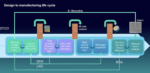
Perforce has published a whitepaper presenting a Transformation Model that provides a blueprint for organizations to navigate this journey. The Model describes five key levels of transformation that organizations have to undergo in order to successfully achieve IP-Centric Design methodology.
Level One: Embracing IP-Centric Design
Design blocks are modeled as intellectual properties (IPs), each with a list of dependencies. This creates a versionable, hierarchical model of the design outside regular data management tools. The definition of IP broadens, encompassing not only pre-packaged design blocks from third-party providers but any block in the design, including those specific to a project, shared between projects, or delivered by central teams.
Level Two: Discovery & Reuse
The modeled IPs, independent of underlying data management, evolve into a dynamic catalog. The catalog allows users to search, filter, and comprehend available IPs based on metadata, irrespective of their location and content. This leads to seamless IP discovery and standardizes project configuration, embedding traceability into the design process. Teams can now make informed build-vs-buy decisions, fostering a culture of reuse that streamlines design efforts.
Level Three: Enterprise Development at Scale
Level Three addresses the challenge of scaling the system to meet the needs of a widespread community of users around the globe. The system must be architected for horizontal scaling, allowing teams to add hardware resources as the team and user numbers grow. Local or near-local response times are critical for effective IP discovery and reuse, especially as different teams collaborate across projects and design centers.
Level Four: Built-In Traceability
The central system becomes the single source of all data and metadata pertaining to designs. Users and workflows can find any design data and metadata they need, ensuring full traceability. This level is crucial for industries governed by standards, where compliance requires proof and provenance of designs. Effective integrations at this level enable organizations to confirm adherence to standards like ISO 26262, ITAR, or CFR21.
Level Five: Planning at Platform Scope
The highest level of IP-Centric Design involves modeling all components of a platform in a unified system. It goes beyond tracking work-in-progress to provide a platform for planning projects and anticipating upcoming needs. This level enables users across the enterprise to view existing IPs and plans for IPs in progress, fostering collaboration, influencing designs, and streamlining efforts across design teams.
Summary
The Transformation Model for IP-Centric Design emerges as a strategic blueprint for success to overcome the challenges of exponential complexity, global collaboration, and intense time-to-market pressures. The journey to IP-Centric Design may seem daunting, but the rewards are undeniable. By taking the first step and partnering with trusted solution providers, organizations can navigate this journey and unlock the full potential. Perforce offers semiconductor solutions that provide the foundation, structure, and scalability necessary for successful implementation. Visit the product page.
Organizations leveraging Perforce can expect improved collaboration, accelerated design cycles, informed build-vs-buy decisions, and streamlined efforts across design teams. Click here to request information.
Also Read:
Chiplets and IP and the Trust Problem