Part 2 of this 4-part series reviews the role of virtual prototypes as stand-alone tools and their use in hybrid emulation for early software validation, a practice known as the “shift-left” methodology. It assesses the differences among these approaches, focusing on their pros and cons.
The Immensity of Software Development the Challenges of Debugging (Part 1 of 4)
Virtual Prototyping and Hybrid Emulation for Early Software Validation
Debugging a software stack for complex System-on-Chip (SoC) designs is a highly iterative process, often requiring the execution of trillions of verification cycles even before end-user applications are considered. For instance, booting Android can take anywhere from 20 seconds to one minute at 1 GHz, depending on the version and end-application, which equates to at least 20 billion cycles. Rebooting this mobile OS ten times a day consumes at least 200 billion cycles. When end-user workloads are factored in, the challenge intensifies, adding more trillions of cycles.
Given the immensity of this task, an effective methodology is essential to support software development teams. Various electronic design automation (EDA) tools and methods are available to address the challenges in response to the exponentially growing demand for processing cycles as one progresses up the software stack.
Hardware Description Language (HDL) Simulators: Viable for Bare-metal Software Validation
At the bottom of the stack, traditional hardware description language (HDL) simulators can be used for bare-metal software validation. However, HDL simulators do not scale with the increasing complexity of hardware designs and the related software complexity. For example, simulating a 100 million gate-equivalent design may advance at a rate of one cycle per second or slower, approximately six orders of magnitude lower than the throughput achievable with hardware-assisted verification engines. This significantly restricts their deployment to block-level or small IP designs, already during the early stages of the verification cycle.
Virtual-based and Hardware-assisted Platforms: Necessary for Early SW Bring-up on SoCs
To meet the demanding requirements of software validation on SoC designs, two primary approaches are prevalent:
- Virtual Prototypes: Extensively used for early software development, testing and validation when Register Transfer Level (RTL) code is still under development
- Hardware-Assisted Verification (HAV) Platforms: Valuable when the RTL is completed, or at least when the necessary hardware blocks and subsystems for software development are available.
Virtual prototypes and HAV platforms possess the processing power to execute billions of verification cycles within feasible timeframes, enabling multiple iterations per hour–or, for very large designs, per day.
Each of these approaches serves different objectives at different stages of the design verification process, providing a balanced solution to the growing challenges in hardware and software development.
Virtual Prototyping: Effective Methodology for Early Software Validation
A virtual prototype is a fully functional software model, typically described in C/C++, that represents an electronic system under development. It can model anything from a single SoC to a multi-die system or an entire electronic system, such as a network of electronic control units (ECUs) in a vehicle. Unlike an RTL model of equivalent functionality, a virtual prototype is considerably slimmer and operates at much higher speeds, often approaching real-world performance. It includes a fast processor model (instruction-set simulator) along with memory and register-accurate peripheral models, all integrated into a binary-compatible representation of the entire system.
Virtual prototypes are ideal platforms for validating the entire, unmodified software stack from bare-metal software to firmware, device drivers, operating systems, middleware, and applications. Their key advantage lies in their early availability during the design cycle, preceding RTL finalization. This early availability enables software engineers to start development in parallel with, or even ahead of, hardware development.
In addition, virtual prototypes can be shared with not only the internal development team but also with technology partners and key customers early in the design process. This collaborative approach allows iterative feedback, enabling external stakeholders to contribute to fine tuning the final product.
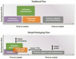
Ultimately, virtual prototypes enable software validation before RTL is available, streamline the development process, and accelerate tape out, resulting in reduced design costs. (See figure 1.)
Virtual Prototyping Commercial Offerings
Today, several electronic design automation (EDA) companies offer virtual prototyping solutions that include libraries of components to address a broad range of design possibilities. The comprehensive nature of these libraries significantly decreases adoption costs for end users, as the modeling effort required for their specific virtual prototypes is substantially lower when most virtual models are readily available off-the-shelf. These solutions also feature robust support for design visualization and software debugging tools, enhancing the users’ ability to develop, analyze, debug, and optimize the software stacks driving their SoC designs effectively.
IP companies play a crucial role in the virtual prototyping ecosystem by supplying models of their IP. For early software validation, models of processor IPs and peripheral IPs are the most relevant.
Some of the leading providers of virtual prototypes include:
Arm
Arm offers a comprehensive catalog of Arm Fast Models (AFM), covering a wide range of processors and system IP. This comprises models for all Cortex processors, Neoverse processors, and various system IP components such as interconnects, memory management units, and peripherals.
RISC-V Virtual Models from IP providers
RISC-V instruction set simulators (ISS) for virtual platforms are available for various RISC-V variants, provided by research institutions and commercial processor IP vendors such as Synopsys, SiFive, Andes or OpenHW. These processor models are primarily based on two technologies, Imperas[1] Fast Processor Models (ImperasFPM) and QEMU (Quick Emulator).
Synopsys RISC-V Models
Synopsys offers the most comprehensive model library of IP Model Library, which includes Synopsys Interface IP, ARC processor IP and leading third-party embedded processor IP. Among them are Imperas Fast Processor Models (ImperasFPM) that cover the complete range of RISC-V standard extensions as well as vendor-specific extensions. Other processors models embrace those from Andes, Codasip, Imagination, Intel, lowRISC, Microsemi, MIPS, NSI-TEXE, OpenHW Group, SiFive, and Tenstorrent. In addition to their use in virtual platforms, these models are used in tools for design verification, as well as for analyzing and profiling RISC-V processors.
Quick Emulator (QEMU)
QEMU is an open-source framework used to create virtual prototypes of complete SoCs, comprising processors and their peripheral models. Open-source initiatives, such as those from Lenovo, are releasing processor models in QEMU for selected processors, such as the Arm Cortex-A series. Additionally, other processor companies are supporting the open-source ecosystem by enabling the creation of QEMU models for their RISC-V cores.
Virtualizer Development Kits (VDKs)
One of the critical barriers to deploying virtual prototypes is the rapid assembly and packaging for easy distribution. The Synopsys Virtualizer tool suite addresses this challenge by providing a large library of IP models, streamlining the creation of virtual prototypes. Teams can further extend and customize these prototypes with their own peripheral models, guided by the tool.
These prototypes can then be packaged as Virtualizer Development Kits (VDKs), which include a suite of efficient debug and analysis tools, as well as sample software. Notably, VDKs integrate seamlessly with leading embedded software debuggers, enabling software bring-up without requiring changes to existing development workflows. VDKs can represent systems ranging from a processor core and SoC to hardware boards and electronic systems, such as a network of electronic control units (ECUs) in a vehicle.
Additionally, Synopsys offers design services to help users fully leverage the capabilities of their VDKs, ensuring they maximize the potential of their virtual prototypes.
Hybrid Emulation: Bridging the Gap for Software Bring-up and Hardware Verification
The hierarchical design process of a SoC begins with a high-level description that assists the design team with multiple tasks. In the initial phase, the high-level description captures the design specifications and intent, enabling early validation of these tasks. Concurrently, it supports early software development through virtual prototyping.
As the design creation process progresses, the high-level description is decomposed into sub-systems and individual blocks, with details added through RTL descriptions. At this stage, co-simulating high-level description of design code and RTL code hinders the speed of execution of virtual prototypes because of the increased complexity of the RTL.
The solution comes through Hybrid Emulation, which leverages the strengths of both virtual prototyping and hardware emulation, creating a powerful synergy that enhances the design verification process.
- Virtual Prototyping excels at high-speed execution, allowing unmodified production software to run on a virtualized version of the target hardware, enabling early software bring-up.
- Hardware Emulation achieves cycle-accurate and fast execution of the RTL blocks and sub-systems, providing a detailed and accurate environment for hardware verification.
While both techniques offer significant speed advantages when deployed in their intended targets, integrating them presents challenges at the interface level where communication between virtual prototypes and hardware emulation occurs. This interface can often become a bottleneck, reducing the overall performance of the hybrid system.
To overcome this, the industry has established the Accellera’s SCE-MI (Standard Co-Emulation Modeling Interface) standard. This standard defines efficient protocols for data exchange between the virtual prototype and the emulated hardware, ensuring reliable, high-speed communication necessary to optimize the hybrid emulation process.
Hybrid Emulation Enables the Shift-Left Verification Methodology
Hybrid emulation enables the concurrent verification of hardware and validation of software by harnessing the fast performance of virtual machines with the accuracy of hardware emulation. The approach speeds up the entire verification and validation process, often referred to as “shift-left” methodology for moving it upstream on the process timeline. Yet, it comes with caveats.
In this hybrid environment, two separate runtime domains arise, each tailored to one of the two tools.
- High-Performance Virtual Prototype: This domain can reach performance of hundreds of million instructions per second (MIPS). The fast environment allows tasks like booting a Linux OS in just a few minutes, compared to over an hour in traditional emulation.
- Cycle-Accurate RTL Emulation: The RTL emulation domain performs at a speed of a few megahertz equating to few MIPS. Although slower, the emulator provides cycle-accurate hardware verification.
The performance disparity between the virtual machine environment and the RTL section can offer speed advantages, particularly for software-bound systems where software execution dictates overall performance. In such cases, the virtual machine can advance rapidly, significantly boosting the speed of software development and testing. Conversely, in hardware-bound systems, where the performance of the RTL code is the limiting factor, the overall speed improvement is minimal. Given that many software development tasks are software-bound, hybrid emulation proves to be highly beneficial for supporting software teams. See figure 2.
Conclusions
Virtual prototyping and hybrid emulation are essential tools for efficient and effective development and debug of the software stack in modern SoC designs. When combined, they form a strategy that embodies the concept of ‘Shift Left’, a shift away from the traditional sequential hardware and software development.
By supporting a unified workflow, the “Shift-Left” methodology encourages close collaboration between hardware and software teams, enabling them to work in parallel, share critical insights, and complement each other’s efforts. This convergence speeds up the verification cycle, uncovers integration issues early on, enhances efficiency, and significantly expedites the time-to-market for SOC development.
[1] Imperas was acquired by Synopsys in 2023.
Also Read
The Immensity of Software Development the Challenges of Debugging (Part 1 of 4)