Synopsys made significant announcements during the recent TSMC OIP Ecosystem Forum, showcasing a range of cutting-edge solutions designed to address the growing complexities in semiconductor design. With a strong emphasis on enabling next-generation chip architectures, Synopsys introduced both new technologies and key updates to existing solutions in collaboration with TSMC.
At the heart of this collaboration is the goal of accelerating the development of trillion-transistor chips, which are necessary to support the computational demands of Artificial Intelligence (AI) and high-performance computing (HPC) applications. As these systems continue to grow in complexity, Synopsys and TSMC are collaborating to leverage AI to streamline the design process and ensure power efficiency, scalability, and system reliability. What caught my interest and attention was the focus multi-die, 3D Integrated Circuits (3DICs), and multi-physics design analysis are receiving in this collaboration. Before we dive into that, below is a roundup of the key announcements.
Roundup of the Key Announcements from Synopsys
Synopsys aims to enable the design of more complex, efficient, and scalable multi-die packages that can meet the evolving demands of AI, HPC, and other advanced computing applications.
Synopsys.ai Suite Optimized for TSMC N2 Process Technology: This was a key update, as Synopsys’ AI-driven EDA suite was already known for its ability to improve Quality of Results (QoR). The latest optimization focuses on the N2 process, helping designers move more swiftly to next-generation nodes while enhancing chip performance and power efficiency.
Backside Power Delivery in TSMC A16 Process: A new innovation that stood out was the backside power delivery system, which promises more efficient power routing and reduced energy consumption. This method helps manage the demands of trillion-transistor architectures by optimizing signal integrity and chip density.
Synopsys IP Solutions for 3DFabric Technologies: Updates were made to Synopsys’ UCIe and HBM4 IP solutions, which are crucial for TSMC’s 3DFabric technologies, including CoWoS (Chip on Wafer on Substrate) and SoIC (System on Integrated Chips). These updates further improve bandwidth and energy efficiency in multi-die designs.
3DIC Compiler, 3DSO.ai and Multi-Physics Flow: One of the more notable announcements involved the enhancement of Synopsys’ 3DIC Compiler platform and 3DSO.ai to address the complexities of multi-die designs and offer AI-driven multi-physics analysis during the design process, helping to streamline system-level integration.
TSMC Cloud Certification for Accelerated Design: To further accelerate the design process, Synopsys and TSMC have also enabled Synopsys EDA tools on the cloud, certified through TSMC’s Cloud Certification. This provides mutual customers with cloud-ready EDA tools that not only deliver accurate QoR but also seamlessly integrate with TSMC’s advanced process technologies.
The Importance of Multi-Die, 3DIC, and Multi-Physics Design
As semiconductor technology pushes beyond the traditional limits of Moore’s Law, multi-die designs and 3DICs have become essential for enhancing performance and density. These technologies allow for multiple dies, each with its own specialized function, to be stacked or placed side-by-side within a single package. However, the integration of these dies—especially when combining electronic ICs with photonic ICs—introduces significant design challenges.
One of the most pressing issues in multi-die design is thermal management. As multiple heat-generating dies are placed in close proximity, the risk of overheating increases, which can degrade performance and shorten the lifespan of the chip. Additionally, electromagnetic interference (EMI), signal integrity, and power distribution present further challenges that designers must account for during early-stage development.
This is where multi-physics analysis plays a critical role. Multi-physics analysis is the process of evaluating how different physical phenomena—such as heat dissipation, mechanical stress, and electrical signals—interact with one another within a chip package. Without an understanding of these interactions, it becomes nearly impossible to design reliable and efficient multi-die systems.
Synopsys Solutions for Multi-Die and 3DIC Challenges
Synopsys is at the forefront of addressing these challenges through its AI-powered solutions, many of which were updated or introduced during the TSMC OIP Ecosystem Forum. These tools are specifically designed to address the complexity of multi-die designs and 3DICs, where early-stage analysis and optimization are crucial for success.
AI-Driven EDA with Synopsys.ai
One of the most significant updates came from Synopsys.ai, which is now optimized for TSMC’s N2 process technology. This suite allows designers to leverage AI to improve design efficiency and reduce the time needed to move designs to production. By incorporating AI into the design process, Synopsys.ai helps engineers navigate the vast array of potential design configurations, ensuring that the most optimal solutions are chosen for performance, power efficiency, and thermal management.
“Synopsys’ certified Custom Compiler and PrimeSim solutions provide the performance and productivity gains that enable our designers to meet the silicon demands of high-performance analog design on the TSMC N2 process,” said Ching San Wu, Corporate VP at MediaTek in Synopsys’ news release. “Expanding our collaboration with Synopsys makes it possible for us to leverage the full potential of their AI-driven flow to accelerate our design migration and optimization efforts, improving the process required for delivering our industry-leading SoCs to multiple verticals.”
3DIC Compiler and 3DSO.ai for Multi-Die Systems
These tools enable designers to conduct multi-physics analysis early in the design process, which is essential for optimizing thermal and power management, signal integrity, and mechanical stability in multi-die systems. By identifying potential issues—such as hotspots or signal degradation—early in the process, designers can make informed adjustments before reaching the later stages of development, thus avoiding costly redesigns.
3DSO.ai leverages AI to analyze complex multi-die configurations, allowing engineers to test a wide range of potential scenarios in a fraction of the time it would take using traditional methods. This capability is critical as designs become more complex, with tens of thousands of possible combinations for how dies are stacked, interconnected, and cooled.
TSMC-certified Synopsys 3DIC Compiler’s compatibility with TSMC’s SoIC and CoWoS technologies further solidify its position as a leading platform for multi-die designs. This ensures seamless collaboration across design architecture and planning, design implementation, and signoff teams, enabling efficient 3DIC development for cutting-edge applications.
These technologies are critical for enabling the heterogeneous integration of dies in 3DIC systems, which helps overcome traditional scaling challenges such as thermal management and signal integrity.
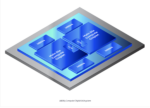
As a demonstration vehicle, Synopsys achieved a successful tapeout recently, of a test chip featuring a multi-die design using TSMC’s CoWoS advanced packaging technology. This test chip leveraged TSMC’s 3DFabric technology and Synopsys’ multi-die solutions, including silicon-proven UCIe IP, 3DIC Compiler unified exploration-to-signoff platform, and the 3DSO.ai AI-driven optimization solution. The Figure below showcases the level of system analysis and optimization enabled by Synopsys 3DSO.ai. The test chip demonstrated unmatched performance reliability.
Figure: Synopsys 3DSO.ai AI-enabled system analysis and optimization
Optimizing Power Delivery with Backside Power Innovations
The new backside power delivery capability, introduced through TSMC’s A16 process, represents a critical leap forward in ensuring power integrity in multi-die systems. By routing power through the backside of the chip, more space is made available on the front for signal routing and transistor placement. This helps reduce energy consumption while also enhancing signal integrity, ensuring that trillion-transistor designs can operate efficiently and reliably.
Summary
The announcements made by Synopsys at the TSMC OIP Ecosystem Forum underscore the growing importance of multi-die architectures, 3DIC systems, and multi-physics analysis in semiconductor design. With new AI-driven tools and key updates to existing solutions, Synopsys is helping engineers overcome the complex challenges posed by trillion-transistor designs and multi-die integration.
By leveraging Synopsys’ advanced EDA tools, platforms and IP, engineers can now address critical issues—like thermal management, signal integrity, and power distribution—at the earliest stages of the design process. This proactive approach not only improves design efficiency but also ensures that the final product meets the stringent performance requirements of AI, HPC, and other next-generation applications.
You can read the Synopsys announcement in its entirety here, and more details on the test chip tapeout here.
Also Read:
The Immensity of Software Development and the Challenges of Debugging (Part 3 of 4)
The Immensity of Software Development and the Challenges of Debugging Series (Part 2 of 4)
Synopsys Powers World’s Fastest UCIe-Based Multi-Die Designs with New IP Operating at 40 Gbps