
At the VLSI Technology Symposium this week Intel released details on their i3 process. Over the last four nodes Intel has had an interesting process progression. In 2019, 10nm finally entered production with both high performance and high-density standard cells. 10nm went through several iterations eventually resulting in i7, a high-performance cell only process. When we characterize process density, we always talk about the highest density logic standard cell, 10nm achieved just over 100 million transistors per millimeter squared density (MTx/mm2), i7 in in 2022 only achieved approximately 64 MTx/mm2 density because it only had high performance cells. i4 entered production in 2023 and is once again a high-performance cell only process and achieves approximately 130 MTx/mm2. Finally, i3 will enter production in 2024 on multiple Intel products providing both high performance and high-density cells. The high-density cells achieve approximately 148 MTx/mm2 transistor density.
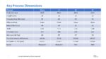
The key dimensions for the processes are compared in figure 1.
Figure 1. Process Key Dimensions Comparison.
In figure 1 the values for 10nm and i7 are actual values measured by TechInsights on production parts, the i4 and i3 values are from the VLSI Technology papers on i4 [1], and i3 [2]. The cell height for i3 of 210nm is for high density cells, there is also a 240nm height high performance cell with the same density as the i4 process. 240nm height high performance cells are 3 fin devices the same at i4 and the 210nm high density cells are 2 fin devices with wide metal zero.
Figure 2 presents the density changes between the processes in graphics form.
From 32nm through 10nm Intel accelerated from 2.0x to 2.4x and then to 2.7x density improvements, but as is the case with other companies pushing the leading edge, i3 is a less than 2x density jump.
Figure 2. Intel Process Density Comparison.
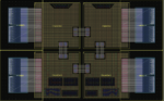
Figure 3 is from the Intel presentation and presents more details on the i4 to i3 process shrink.
Figure 3. i4 to i3 Process Shrink.
The i3 process will offer multiple variants targeted at different applications.
- i3 base process and i3-T with TSVs targeted at client, server and base die for chiplet applications.
- i3-E offer native 1.2 volt I/O devices, deep N-wells, and long channel analog devices, and is targeted at chipsets and storage applications.
- i3-PT targets high performance computing and AI with 9μm pitch TSVs and hybrid bonding.
Figure 4 summarizes the process variants.
Figure 4. i3 Process Variants.
i3 features:
- Smaller M2 pitch than i4.
- Better fin profile.
- Utilizes dipoles to set threshold voltages, i4 does not use dipoles. Dipoles improve gate oxide reliability.
- Offer 14, 18, and 21 metal layer options (counts include metal 0).
- 4 threshold voltages, V:VT, LVT, SVT, HVT.
- Contact optimization to provide less overlap capacitance.
- More effective EUV usage, i4 was Intel’s first EUV process, i3 EUV processes are less complex.
- Lower line resistance and capacitance than i4.
- 5x lower leakage at the same drive current as i4.
- Increased frequency and drive current with no hot carrier increase.
- Interconnect delay is now approximately half of overall delay and the base process has better RC delay, the PT process is even better.
- At the same power i3 HD cells provide 18% better performance than i4 HP cells.
Figure 5 presents the interconnect pitches for the 14, 18, and 21 metal options.
Figure 5. Interconnect Pitches.
Figure 6 illustrates the improvement in interconnect RC delay.
Figure 6. Interconnect RC Delay.
And finally, figure 7 illustrates the 18% performance improvement over i4.
Figure 7. Interconnect Delay Improvement.
During an analysts briefing session questions and answers session Intel disclosed the channels are all silicon, no silicon germanium channels. Also, i4 designs have been ported to i3 and they are seeing PPA improvements on the same designs.
i3 is currently in high volume manufacturing with multiple Intel products.
i3 clearly represents a significant improvement over i4.
Comparisons to competitors
i3 is a significant improvement over i4 but how does it compare to competitors?
TechInsights has analyzed density, performance, and cost of i3 versus Samsung and TSMC processes. That analysis is available in the TechInsights platform here (free registration required):
Conclusion
Intel’s i3 process is a significant step forward from Intel’s i4 process with better density and performance. Intel’s i3 process is a more competitive foundry process than previous generations. Cost is more in-line with other foundry processes, density is slightly lower than Samsung 3nm and much lower than TSMC 3nm, but it has the best performance of the “3nm” processes.


