

We have been working with Ansys since SemiWiki was founded in 2011. It has been a richly rewarding relationship in all regards. I always say the semiconductor industry is filled with the most intelligent people in the world and Ansys is an excellent proof point. I have known John Lee for 30+ years and he is one of my trusted few, absolutely.
Tell us a little bit about yourself and your company.
I have been an EDA person for most of my career. I was really blessed to be a graduate student of Professor Ron Rohrer at Carnegie Mellon University, in a research group that launched the careers of many highly successful students, including three CEOs and two Kaufman Award winners.
I’m also blessed to be part of Ansys. We have over 6,000 employees worldwide and our products power innovation that drives human advancement across a very broad array of industries and technical challenges. For example, we have an ongoing partnership with Oracle Red Bull Racing to help them remain the most competitive Formula 1 (F1) team in the world. Oracle Red Bull Racing used Ansys Fluent for streamlining simulations, Ansys Granta for optimizing material choices, and Ansys LS-DYNA to verify safety parameters. They were able to design and optimize a race car that driver Max Verstappen used to make history in 2023, winning 21 out of 23 races and secure the Drivers’ and Constructors’ Championships with a massive 413-point margin.
Another example is how NASA engineers used capabilities from Ansys AGI to steer the James Webb Telescope by simulating the complex gravitational perturbations acting on its orbit and estimate station-keeping requirements. The project also relies on Ansys Zemax optical simulation to align the segmented mirror optics and Ansys Mechanical to model the natural vibration modes of the mirror as it is being pointed.
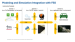
I hope these examples give you an idea of the amazingly broad range of physics simulation solutions supported by Ansys, which include Thermal, Mechanical, Semiconductors, Electromagnetics, Optics, Photonics, Fluid Dynamics, Acoustics, 3D Design, Materials, Safety, Digital Twins, Autonomous Vehicles, Embedded Software, and Mission Engineering.
My responsibility at Ansys is for the Electronics, Semiconductors and Optics products. Our focus has been very rewarding, as the need for open and extensible Multiphysics platforms and solutions has become very clear over the last five years. We’ve been fortunate to establish ourselves as both thought leaders and trusted partners with market-shaping customers.
What was the most exciting high point of 2023 for your company?
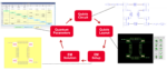
The rapid adoption of 2.5D and 3D heterogeneous designs has been both very challenging and very rewarding. Many of these systems are being driven by the AI revolution. These systems consume massive amounts of power, which naturally generates tremendous thermal effects, which induce mechanical effects such as stress and strain that affect both performance and reliability.
The thermal-centric challenges of 3D-IC are even more profound, and if you look at the new systems being designed by the leaders in AI, you can see why 2023 was very exciting and rewarding for Ansys.
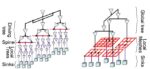
A beneficiary of this work is that the AI methods we’ve developed at Ansys are further accelerated. For example, we combined AI with our revolutionary sigmaDVD technology in RedHawk-SC, to enable significantly better PPA from place and route tools. Our leading customers deployed this in 2023, and we see accelerated adoption in 2024. As power and thermals strongly affect advanced process node design, using AI + sigmaDVD has become a very, very exciting high point!
What was the biggest challenge your company faced in 2023?
Ansys has grown significantly during the pandemic, both organically and inorganically. Since 2020, for example, we’ve announced 10 acquisitions, and we’ve grown rapidly in new offices, including Athens, Vancouver, and Rwanda!
So, figuring out how to onboard many new hires across many regions and also integrate great high-performing teams from our acquisitions has been a challenge and focus of mine in 2023.
How is your company’s work addressing this biggest challenge?
Culture and engagement have been a real focus on the leadership team at Ansys before, and especially during the pandemic. It has been very rewarding to see the focus on this challenge pay off. For example, we are proud that the Wall Street Journal named Ansys one of the 250 best-managed companies of 2023, and Newsweek recognized Ansys as one of the top 100 Most Loved Workplaces.
What do you think the biggest growth area for 2024 will be, and why?
The insatiable and pervasive demand for compute is driving the convergence between silicon and systems, which is creating great opportunities for companies like Ansys.
First, there is an accelerated need for open and extensible Multiphysics platforms – such as Ansys AEDT and SeaScape (for system and chip designers) to partner with leading design platforms – and our investments in the areas of physics, platform and partnerships is driving deep customer value.
Second, both semiconductor and system companies are focused on the benefits of optimized software + silicon systems. This is occurring in automotive, with software defined vehicles; in communications, with 5G and 6G systems; and in the data center, with power and thermal limited compute. Concepts which are missing from the EDA lexicon – such as MBSE, SPDM, SIL and digital twins – are a big opportunity for companies like Ansys.
How is your company’s work addressing this growth?
The Ansys team and portfolio is a great combination of core physics, advanced computational sciences (including AI, cloud and platform), and system-level products that deliver on the need for model-based systems engineering, functional and cyber-security, powerful digital twin models between component and system designers. You’ll see many exciting announcements in this area this year!
What conferences did you attend in 2023 and how was the traffic?
We’ve been excited by the interest in co-packaged optics (CPO), which is a key trend for anyone designing products for the data center and AI. So, Photonics West and Optical Fiber Conference (OFC) were great.
DesignCon is another event that has really rebounded since the pandemic, and the convergence between silicon and system is driving lots of interest in Ansys Multiphysics.
Will you attend conferences in 2024? Same or more?
Mobile World Congress is one that we just came back from, and it’s been exciting to see how Ansys technologies are helping 5G communication systems deploy using our Ansys RF Channel Modeler and AGI Systems Toolkit (STK). For classic EDA folks like me, it’s very exciting to see how computational physics and missions planning are playing a vital role in connecting the world.
Also Read:
Ansys and Intel Foundry Direct 2024: A Quantum Leap in Innovation
Why Did Synopsys Really Acquire Ansys?


