The Impact of the AI Revolution on the Server Manufacturers
While some will designate my research as market research, I view it differently. Having done and bought plenty of market sizing research, I have not seen it lead to any change in behaviour or strategy. It has been used to confirm a strategy already decided and the “great” performance of divisions and vice presidents.
If it pointed towards lower market share or lower divisional performance, you would come under attack, and more appropriate (confirming) research would be selected so people could get back to executing the strategy decided.
There’s a prevailing sentiment: ‘Don’t disrupt our strategy with facts’
Also, most market research is an Excel exercise done by an entry-level employee in isolation from other research. It is already outdated when sold, and calling it data would be a stretch.
For most companies, a strategy is a fixed plan that spans decades and gets adjusted now and then. This approach is straightforward for people to understand and adapt to but ignores that strategy is a response, and in a business setting, strategy is a response to a change in the marketplace.
Strategy is a response to a change in the marketplace
Even if the strategy is market-defining as Nvidia’s entry into AI, it is still a response to the marketplaces from which the new market is rising.
I do strategic market research, not market-sizing research. The size of the market rarely matters. Would you do anything different if you knew you had 10.8% market share or 14.3%? Market size does not change your strategy, but market change should, especially if the change in the market right now is as disruptive as the AI change.
Market change should drive strategy, not market size
A good strategy starts with the question: What is going on? What is changing? It is then built around a response that is within the company’s capabilities and protects it against change or exploits new opportunities arising from the change.
In other words, strategy is all about timing. But you already knew that. You have done things too early and too late before. Like most other strategies, a sound investment strategy relies on the proper timing of trades. The same goes for business strategies.
“A fairytale remains a fairytale only when you close the book at the happiest moment; Timing is everything.”
Intel’s strategy was incredibly successful until it was not. Intel’s response to EUV and the AI revolution in the data centre came too late, as Intel has not been used to responding to changes in the market. The company is now in a situation where its fate is in other people’s hands.
The current AI revolution is not creating soft waves in the fabric of the semiconductor supply chain; it is a tsunami that changes everything. This will decide winners and losers in all areas of the supply change for years to come. Ride the tsunami with us and gain insights for your strategic response.
The Screwdriver Circus
Years ago, a good friend in deep Russia commented on an electronics subcontractor: “They are just a screwdriver circus!”
While I don’t think negatively about electronic subcontractors, they are certainly a different game than semiconductors. Electronic Manufacturing Services (EMS) must live on small margins while managing significant purchasing risk. EMS is very exposed to market changes, and its response is usually immediate.
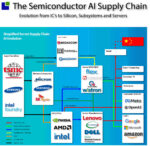
The AI revolution, in general, and Nvidia, in particular, has significantly changed all aspects of the Semiconductor supply chain and also impacted the manufacturing side of it.
Nvidia is no longer only selling Chips; the company sells a mixture of chips, GPU subsystems, and complete Server racks. They are no longer just buying silicon but also memory, components, power, chassis, and assembly.
In the good old days (a year ago), TSMC sold silicon to Nvidia, Nvidia sold Chips to a server manufacturer that also bought memory, power, network, chassis and other stuff to make a server.
This has all changed
The new supply chain is significantly more complex and lacks traditional chips. These have been replaced by GPU Subsystems, including high-bandwidth memory and networking.
Nvidia sells its own servers manufactured at the EMS/ODMs. At the same time, it sells its GPU subsystems to Server manufacturers, which make them into branded servers.
Lastly, they sell their GPU subsystems to end customers who use EMS/ODMs to create server systems that fit their needs.
The largest server customers are all designing their own accelerator chips for different workloads, which the Nvidia servers excel at. These are developed with companies like Broadcom, Marvel and Qualcomm using Silicon from the logic foundries. Like the GPU/CPU subsystems, these accelerator subsystems include memory and networking components.
These subsystems are installed into custom server systems controlled by the principal owner of the architecture. The best-known principals are:
- Amazon (Inferential, Trainium)
- Google (TPU)
- Microsoft (Maia)
- Meta (MTIA)
The cloud of Increasing Complexity
The increasingly complex supply chain makes it difficult to understand what is happening in the AI Supply chain. Most stakeholders can brush this off and state: “Fortunately we are not in the AI game”.
The problem with that attitude is that the AI supply chain is disrupting all other semiconductor and electronic manufacturing chains at the moment:
The most important foundry is transforming into a leading node only supplier.
The Memory companies are moving capacity to HBM making it difficult to maintain capacity for standard memory.
The manufacturing sector is prioritising AI servers with higher margin.
The AI embargos is making China the go to place for mature tech.
We believe the AI disruption of the supply chain will affect everybody and they will need to pay attention to what is changing and what Strategy they need to adapt.
As alway, I enjoy this complexity and take the opportunity to take a deeper dive into areas of the supply chain to uncover insights that can be used for strategy formation. The focus in this post will be on the server manufacturers.
The Server manufacturers
The top 5 server manufacturers are in the middle of the AI storm and are no longer surprised by the rapid need for higher power liquid cooled AI servers. You would expect that you could see it on their overall revenue, but you will be disappointed.
There is no visible change in revenue or in Gross and Operating profits other than revealing that this is a low margin business.
So we could stop the analysis here and conclude that nothing dramatic is going on. But “nothing” is not what I would expect so I continued the analysis.
While the overall revenue (including other products that servers) reveal no impact of the AI revolution, both the increasing cost of goods sold (COGS) and the increasing inventory position that something is going on.
This is likely because the BOM for AI systems are higher, impacting the working capital position and tying up more inventory for the AI servers.
The revenue by company reveals that there is some movement between the top 5 Server companies.
Super Micro Computer and Inspur EII, both pure play server companies are outgrowing the 3 larger competitors that have other revenue.
The Server based view
Isolating the server based revenue shows that the server business is indeed growing significantly and in particular Super Micro is in rapid growth mode.
Supermicro has moved from number 5 to number 2 in a little over a year and is very close to Dell in terms of Server revenue.
Revisiting COGS and Inventory for the server business alone, shows the dramatic increase in inventory and COGS. If the increase in revenue was from standard servers, COGS and Inventory would follow the revenue growth. So the acceleration we are seeing is from AI servers and the inventory points to future rapid growth of AI.
In order to understand the AI element of the server business we exclude Inspur from the following analysis as there is no credible data on their AI business.
The top 4 Server companies
Without Inspur, the Top 4 Server companies have a total server revenue of 17.5B$ in Q2-24. As Dell and HPE already has reported Q3 numbers that showed 29% growth in total, it would be surprising if the top 4 Server revenue is not a new significant record. If Lenovo and Super Micro has similar growth numbers, the top 4 revenue will grow to 22.5B$.
The revenue growth is totally dominated by the AI server revenue as can be seen below. Dell and HPE are showing close to 70% quarterly growth from Q2 to Q3. We are seeing a significant inflexion point in the business of the server companies.
The non AI part of the Server revenue is contracting even though Dell reported a Q3 increase in non AI Server based revenue.
The AI server share of server revenue reached 43%, up from 4% in the beginning of 2023.
The last two chart are important for Nvidia’s growth thesis that is described in the post below:
Nvidia Pulled out of the Black Well
There have been serious concerns about the ROI on AI and yield problems with Blackwell, but Nvidia pulled it off again and delivered a result significantly above guidance.
Jensen Huang believe that the AI server revenue will not only be on top of the existing CPU based data center infrastructure but also also replace a significant part of it. Our analysis shows that Jensen’s growth thesis could be valid as the non-AI server revenue is indeed declining not only in share but also in absolute $ terms.
This is still to early to conclude but is going to be something I follow from now on.
Conclusion
Hidden by flat overall revenues, the AI revolution is now also showing a massive impact on the numbers of the server companies. AI now represent 43% of the overall server revenue and the traditional Server revenue is in decline.
The server revenue is driven by the CPU/GPU architectures from Nvidia, Intel and AMD while the accelerator revenue will materialise through the EMS/ODM’s.
With the increasing AI share, the Server companies need to handle more power and Direct Liquid Cooling and the increasing costs are pushing up the COGS and the inventory position. This has limited the profit growth of the AI business up until now. Once fully adapted to AI and DLC, the profits will begin to increase.
While China seems to be able to get both high end and low end AI, the channel(s) are not revealed yet although we have some pretty good candidates. The flow of AI to China, has also impacted the internal development of GPU’s in China. The chinese GPU leader Xiangdixian Computing Technology, is in problems and has to scale down operations significantly.
Pledge your support for this content
Also Read:
The Semiconductor Business will find a way!
Nvidia Pulled out of the Black Well
The State of The Foundry Market Insights from the Q2-24 Results


